


Damage-free dry transfer printing of ultrathin films with on-demand interfacial adhesion: principles and applications
 0
0 Abstract
Transfer printing, a foundational manufacturing route for integrating heterogeneous materials onto diverse substrates, holds great promise for applications in flexible electronics, emerging displays, and soft robotics. As applications grow more complex, the quality of ultrathin films integrated onto applicable substrates, initially fabricated on rigid substrates by spin-coating, physical vapor deposition, or chemical vapor deposition [e.g., photoresists, metals, two-dimensional (2D) materials] with thicknesses below 10 μm, becomes critical to the performance of advanced devices, including flexible/curved electronics and 2D films-based electronics. However, achieving damage-free transfer printing of ultrathin films requires resolving the trade-off in traditional methods between interfacial fracture and in-plane film damage. Herein, this review elucidates the principles underlying damage-free transfer printing of ultrathin films, highlights recent innovations that enable on-demand control of interfacial adhesion during the process, and summarizes typical applications based on transferred damage-free films. Finally, we provide perspectives on the remaining challenges and future developments needed to enable industrial-scale manufacturing and inspire continued innovation.
Keywords
INTRODUCTION
Over the past two decades, transfer printing has emerged as a transformative manufacturing method for heterogeneous integration on arbitrary surfaces[1,2]. The process consists of two decoupled steps: first, functional materials are patterned on donor substrates using high-resolution micro/nanofabrication techniques[3,4], such as photolithography, electron-beam lithography, physical vapor deposition (PVD), and chemical vapor deposition (CVD); second, the patterned materials are picked up with a stamp and printed onto receiver substrates. Initially focused on integrating robust materials (e.g., semiconductor membranes[5,6], microchips[7-9]), transfer printing methods have matured and become essential for next-generation flexible electronics[10,11], optoelectronics[12,13], and soft robotics[14]. A pivotal advance came in 2006, when Meitl et al. introduced elastomeric stamps with kinetic adhesion control to integrate semiconductor membranes[1]. Researchers then systematically reported the interfacial dynamics of elastomeric stamps, including contact velocity[15,16], contact area[17,18], peeling radius[19,20], and shear force[21,22], to modulate adhesion and achieve reliable transfer of membranes/microchips. Building on this foundation, smart stamp-based methods have engineered bioinspired micro/nanostructuring on stamp surfaces, drawing on adhesives from aphids[23,24], octopuses[25,26], and geckos[27,28] to achieve directional, reversible, and selective transfer, with notable impact in laser-driven transfer printing systems[29-31]. Moreover, smart stamps composed of stimuli-responsive materials provide on-demand adhesion switchability under thermal, optical, or electrical triggers, expanding the versatility and application scope of transfer printing[32-34]. Recent advances in flexible/curved electronics and two-dimensional (2D) films-based electronics increasingly rely on damage-free ultrathin films as critical components, serving as sensing interfaces and charge transport layers[35-38]. However, their development is constrained by incompatibilities of existing fabrication processes. These ultrathin films (typically < 10 μm) are initially formed on rigid donor substrates via spin-coating, PVD, or CVD, such as photoresist films, metal films, and 2D films[39-42]. Achieving uniform ultrathin photoresist films directly on flexible/curved surfaces remains difficult, limiting high-resolution fabrication of flexible/curved electronics[43]. Moreover, 2D films have low damage thresholds and cannot withstand energetic ion bombardment during metal deposition, which degrades metal-2D semiconductor contacts[44]. Though intact growth of 2D materials on donor substrates is routine, picking up these films requires etching the growth substrates, leading to solvent contamination[45,46]. Traditional transfer printing partially mitigates incompatibilities, but transfer printing of ultrathin films without damage remains challenging: the stress inevitably generated during peeling can exceed the fracture resistance of the ultrathin films and that of the film/substrate interface, leading to in-plane fractures, cracking, or delamination. Such structural damage compromises ultrathin film integrity, reduces manufacturing yield, and degrades device performance[47].
Several methods, including wet and dry transfer printing, have been developed to integrate ultrathin films onto various substrates. In wet transfer printing, sacrificial layers such as water-soluble polyvinyl alcohol (PVA) and solvent-soluble polyacrylic acid (PAA) are commonly used[48]. The 2D films grown on substrates [e.g., copper (Cu)] require removal of the growth substrate by wet etching, followed by transfer to the receiver substrate[45,46]. However, liquid-phase processing introduces hydrodynamic instabilities that can cause film damage (e.g., fractures and delamination), compromising the structural integrity and functional reliability of the transferred ultrathin films. To address this issue, Le Borgne et al. reported a water transfer printing method[49]. Ultrathin films patterned on PVA floated at the water surface upon dissolution of the PVA layer due to surface tension and can be seamlessly laminated onto immersed objects[49,50]. Despite its utility, PVA is a challenging fabrication substrate because its solubility and surface properties complicate the formation of ultrathin films. While some approaches have attempted to fabricate films directly or indirectly on such sacrificial layers[51,52], they often add process complexity, leading to inconsistent yields and scalability challenges. Generally, despite difficulties in process control and reproducibility, wet transfer printing remains a promising route for conformal manufacturing of ultrathin films in advanced applications.
Unlike wet transfer printing, dry transfer printing offers rapid, sustainable operation for transferring ultrathin films using simple mechanical means. A typical dry transfer printing system involves three critical interfaces: film/donor substrate, film/stamp, and film/receiver substrate. Theoretical models and experiments show that successful transfer printing is governed by competition among the interfaces’ critical energy release rates (Gcrit)[2]. For pickup [Figure 1A], the critical energy release rate at the film/stamp interface (
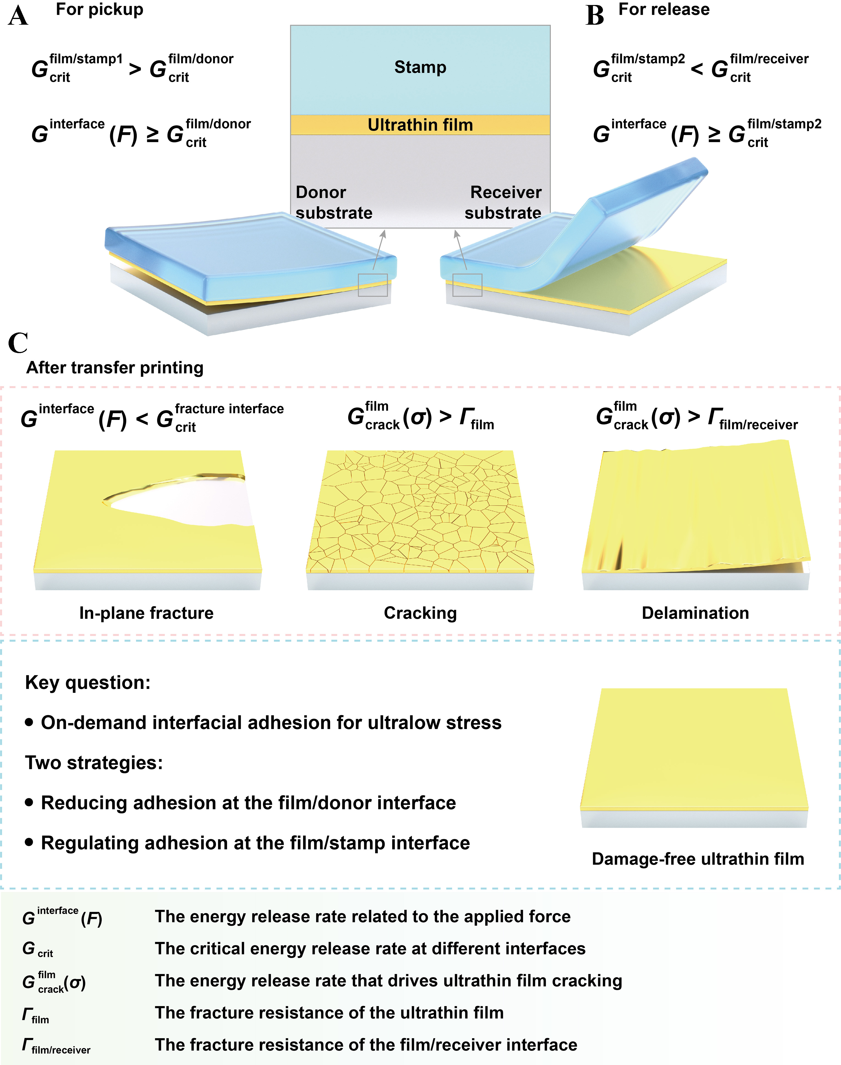
Figure 1. Schematic illustration of damage-free dry transfer printing for ultrathin films. The transfer printing system consists of a donor substrate, ultrathin films, a stamp, and a receiver substrate, where successful transfer depends on the fracture energy competition at interfaces. (A) For pickup, it must satisfy
As a foundational technology for heterogeneous integration, transfer printing has received significant attention in recent reviews, covering stamp adhesion modulation[57-59], microstructured stamps[27], material systems[60], and applications in flexible electronics[10,11,61], curved electronics[62,63], optoelectronics[12,13,47], and energy devices[64,65]. However, these reviews only partially address damage-free dry transfer printing of ultrathin films. To fill this void, we systematically review the strategies and underlying principles for achieving damage-free dry transfer printing with on-demand interfacial adhesion. We further evaluate applications in which damage-free ultrathin films are pivotal, including flexible/curved electronics and 2D film-based electronics. Finally, we outline challenges and perspectives, emphasizing the need for industrial-scale manufacturing to advance emerging technologies.
STRATEGIES AND PRINCIPLES
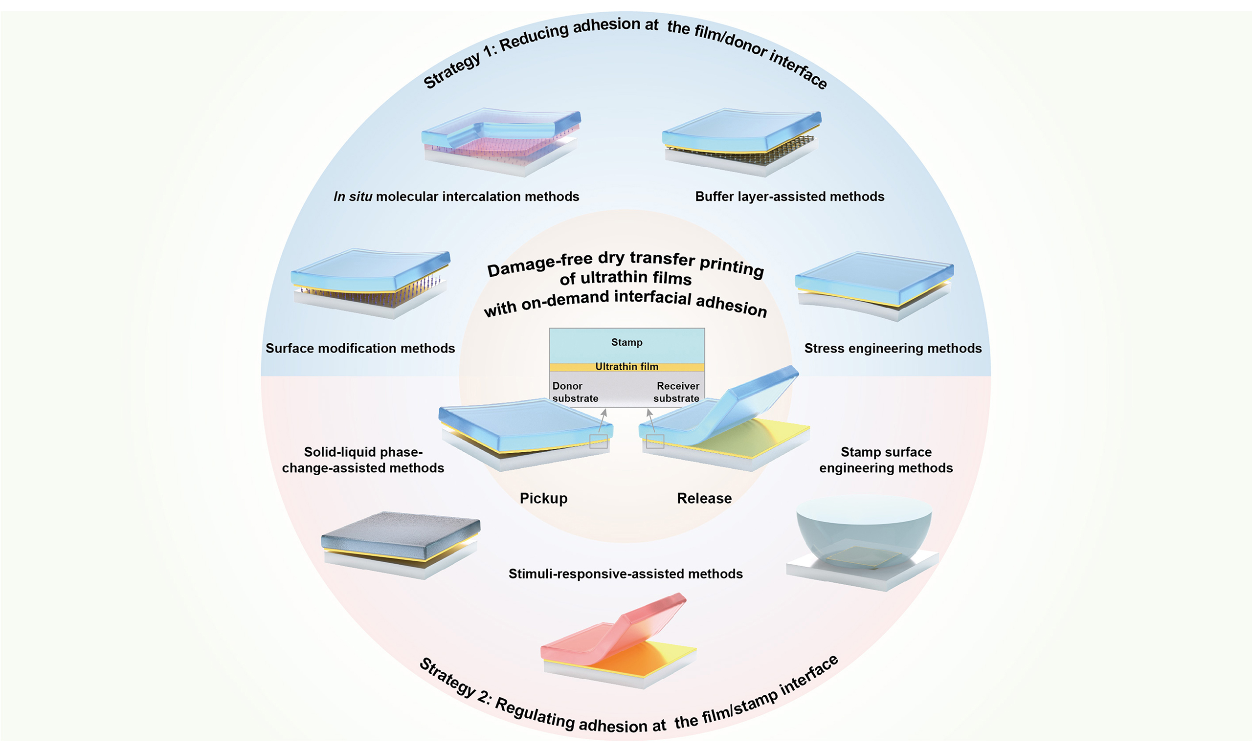
The criteria, typical strategies, and applications for modulating on-demand interfacial adhesion to achieve damage-free transfer printing of ultrathin films are outlined in Figure 2[66-70]. Broadly, these strategies fall into two categories: (1) reducing adhesion at the film/donor interface and (2) regulating adhesion at the film/stamp interface, both aimed at minimizing peeling stress during transfer printing. At the film/donor interface, chemical modification of the donor substrate is a widely adopted route to reduce adhesion. Alternative approaches, such as in situ molecular intercalation methods, buffer layer-assisted methods, and stress engineering methods, also show potential for creating near-zero-adhesion interfaces. At the film/stamp interface, adhesion is regulated using smart stamps with on-demand switchability. Examples include solid-liquid phase-change-assisted methods, stimuli-responsive-assisted methods, and stamp surface engineering methods, which enable interfacial adhesion to be regulated by external triggers. The principles, advantages, disadvantages, ultrathin film materials, applicable substrates, and typical applications of each technique are summarized in Table 1, and their practical implementations are systematically discussed in the subsequent section.
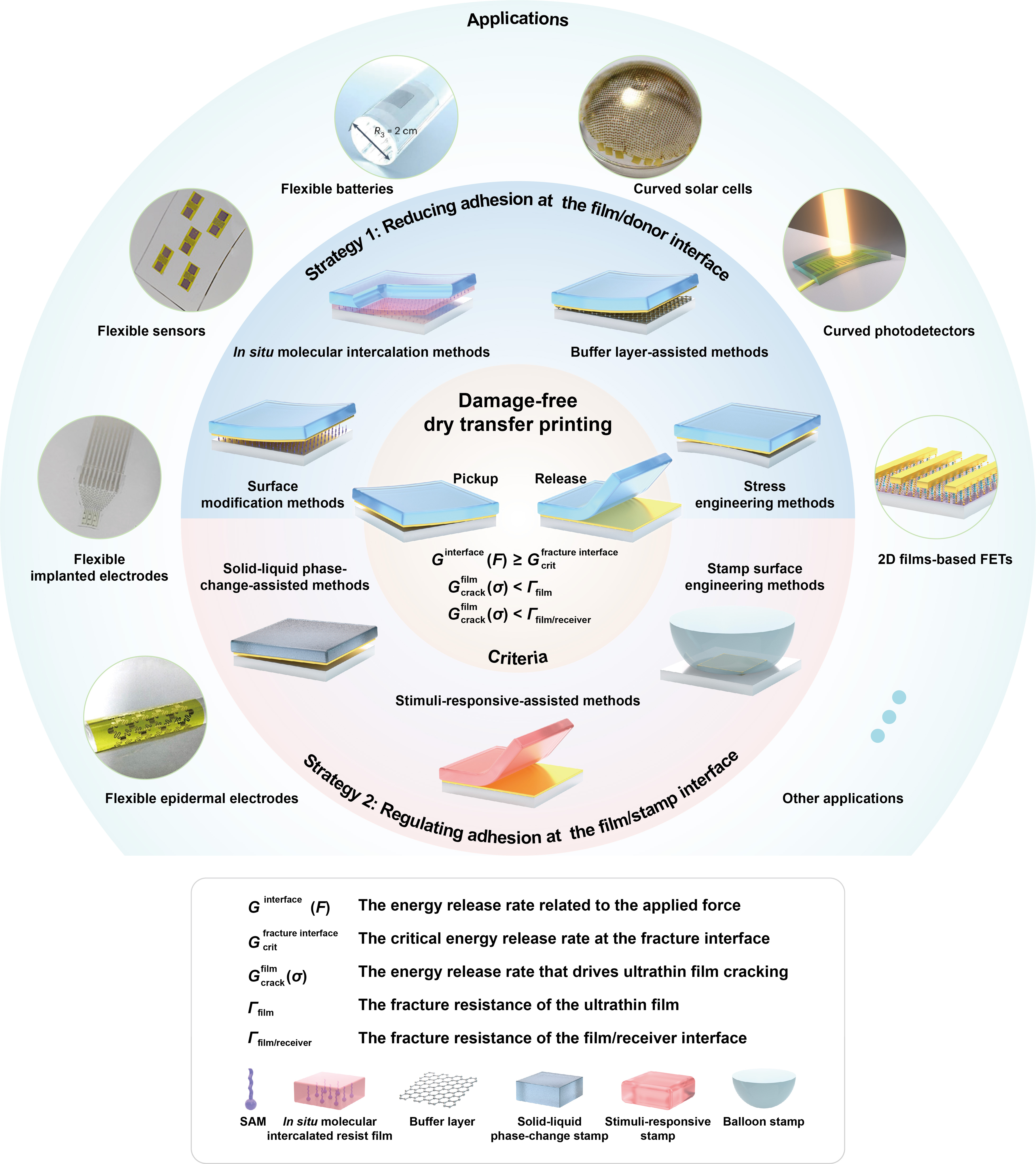
Figure 2. Criteria and typical strategies for modulating on-demand interfacial adhesion in damage-free dry transfer printing of ultrathin films and applications in flexible epidermal electrodes[66], flexible implanted electrodes[67], flexible sensors[68], flexible batteries[69], curved solar cells[70], curved photodetectors, 2D films-based FETs, and other applications. Reproduced with permission[66]. Copyright 2024, American Chemical Society. Reproduced with permission[67]. Copyright 2017, WILEY-VCH. Reproduced with permission[68]. Copyright 2020, The American Association for the Advancement of Science. Reproduced with permission[69]. Copyright 2024, Springer Nature. Reproduced with permission[70]. Copyright 2019, Springer Nature. FETs: Field-effect transistors.
The summary of damage-free dry transfer printing depended on the strategies for regulating interfacial adhesion, including principles, advantages, disadvantages, ultrathin film materials, applicable substrates, and typical applications
| Main methods | Principles | Advantages | Disadvantages | Ultrathin film materials | Applicable substrates | Typical applications | Ref. |
| Strategy 1: Reducing adhesion at the film/donor interface | |||||||
| Surface modification | SAMs offering a low-energy surface | No influence on ultrathin films | Need specific molecular interactions and precision control for spin-coating resist films | Photoresist: PMMA Metal: Cu, Au, Ni, Zn Metal oxide: MnO2 Metal sulfide: CdS Polymers: PPy, PANi | Curvy Suspended Flexible Stretchable MoS2/SiO2 | Transistors Flexible electrodes Flexible display | [71,72] |
| In situ molecular intercalation | Self-organized amphiphilic molecules building a low-adhesion interface | Easy spin-coating and peeling | Limited by the range of compatible resists | Photoresist: SU-8, PMMA, PVA, RZJ-390PG | Curvy Degradable Flexible Stretchable MoS2/SiO2 | Metalens Flexible electrodes | [43,73-75] |
| Buffer layer-assisted | A buffer layer offering a low adhesion interface | Able to transfer high-adhesion metals | Low yields due to defects in the buffer layer | Metal: Cu, Ag, Au, Pt, Ti, Ni | MoS2/SiO2 | Transistors Flexible display | [44,76] |
| Stress engineering | Stress-engineered interface building a low-adhesion interface | Preserving the integrity of ultrathin films | Constrained by the narrow range of transferable materials | Metal: Pt, Cu, Au, Ti ALD-oxide | Curvy Suspended Flexible Stretchable | Curvy sensors Flexible thin-film battery Transistors | [69,77] |
| Strategy 2: Regulating adhesion at the film/stamp interface | |||||||
| Solid-liquid phase-change-assisted | Different phases of the stamp showing a large adhesion change | Large adhesion switchability | The liquid involved may limit the kinds of ultrathin films | Metal: Au, Pt, Ni Metal oxide: MoS2 Hybrid: metal on PI | Curvy Biological | Transistors Flexible sensors | [78-80] |
| Stimuli-responsive-assisted | The stamp’s adhesion switched in response to external stimuli | Easy operation, low cost | External stimuli may influence the ultrathin films | Metal: Au, Pt Hybrid: metal on PI | Curvy Biological MoS2/SiO2 Flexible Stretchable | Transistors Flexible electrodes Curvy sensors | [66,67,81,82] |
| Stamp surface engineering methods | Chemically or physically regulating the adhesion | Applicable for 3D curved surfaces | Limited by the receiver substrates’ material | Hybrid: metal on PI | Curvy | Curvy solar cell Curvy antenna Curvy sensors | [70] |
Reducing adhesion at the film/donor interface
Ultrathin films formed on rigid donor substrates by spin-coating, PVD, or CVD typically exhibit robust interfacial bonding, such as van der Waals (vdW) forces, diffusion, and chemical bonds[83]. These strong interactions pose challenges during the film detachment[71]. Strong adhesion at the film/donor interface necessitates a larger Ginterface(F), which elevates in-plane stress within the film. When
Surface modification methods
Self-assembled monolayers (SAMs) are generated via intermolecular interactions between organic molecules and the substrate surface physically or chemically[84,85]. Typically, one terminus bears a high-affinity anchor group that forms strong, directional bonds with the donor substrate (e.g., silanes for oxide[86], thiols for gold[87,88], phosphonates for metal oxides[89]). In contrast, the opposing terminus carries tailored functional groups that can be engineered to enable weak adhesion to ultrathin films, ensuring damage-free pickup under ultralow force [Figure 3A].
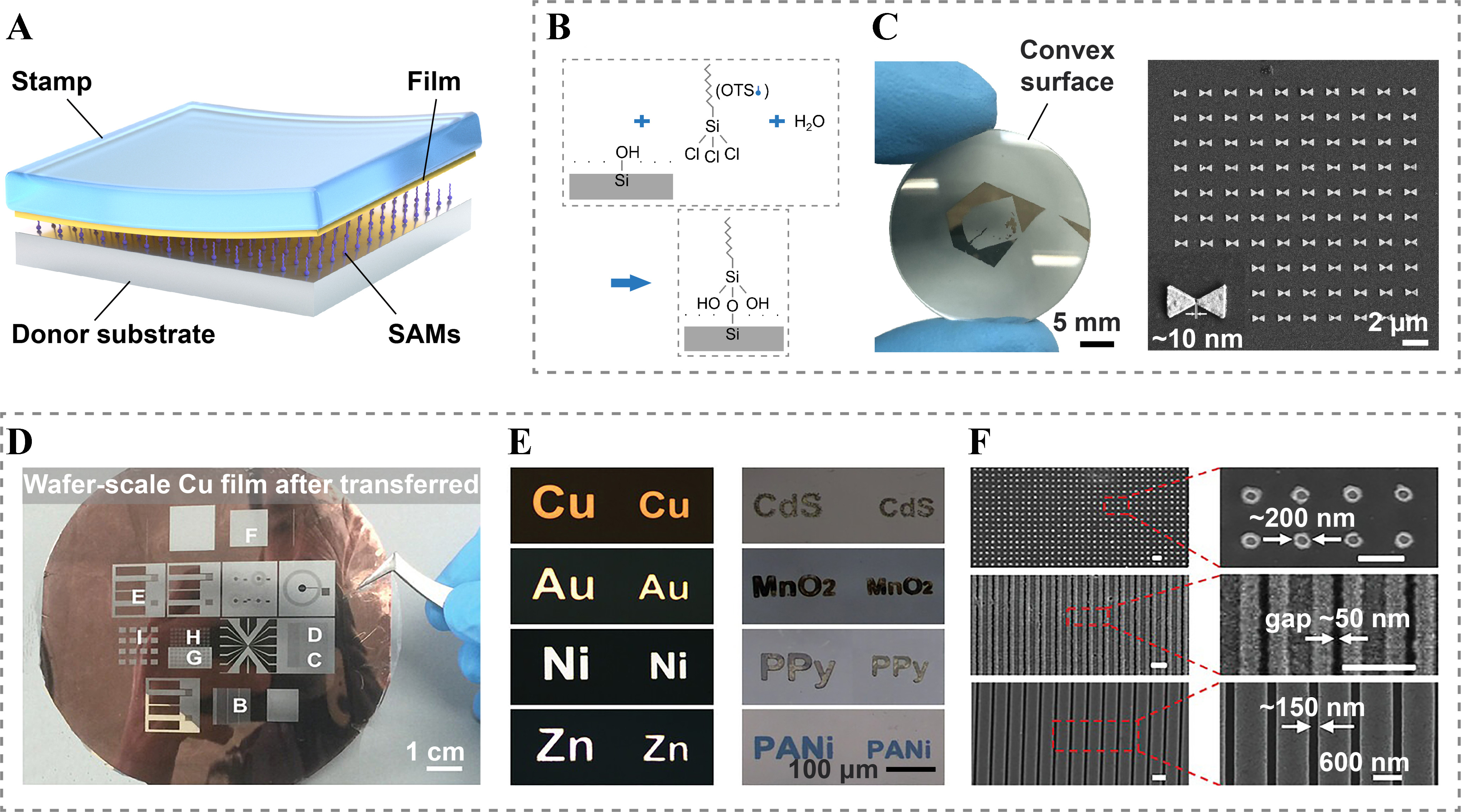
Figure 3. Reducing adhesion at the film/donor interface based on surface modification methods for damage-free transfer printing of ultrathin films. (A) Schematic illustration showing the dry pickup process enabled by the prior construction of a SAM layer on the donor substrate; (B) Schematic diagram illustrating the molecular mechanism of OTS chemisorption on a silicon surface; (C) Optical and SEM micrographs of Au nanostructures after being transferred onto a convex surface. Reproduced with permission[71]. Copyright 2023, IOP Publishing; (D) A 4-inch wafer-scale Cu pattern fabricated by the ERT method; (E) The ERT method is applicable to a wide variety of materials: metals (Cu, Au, Ni, and Zn), metal oxide (MnO2), metal sulfide (CdS, semiconductor material), and polymers (PPy, PANi); (F) SEM images of different nanoscale patterns using the ERT method. Reproduced with permission[72]. Copyright 2023, Wiley-VCH. SAM: Self-assembled monolayer; OTS: octadecyltrichlorosilane; SEM: scanning electron microscope; ERT: electrochemical replication and transfer; PPy: polypyrrole; PANi: polyaniline.
Silane SAMs modification methods
Silicon (Si), the predominant semiconductor substrate, supports SAM formation through surface hydroxyl groups with silane-terminated molecules, yielding a low-energy surface that reduces adhesion to resist films[90]. Shu et al. introduced a near-zero-adhesion approach for wafer-scale, intact resist film transfer printing[71]. Central to this approach was establishing a critical surface energy window via octadecyltrichlorosilane (OTS) SAM modification of the Si substrate to minimize adhesion between the resist film [e.g., polymethyl methacrylate (PMMA)] and the donor. OTS molecules selectively reacted with surface -OH on Si to form covalent Si–O–Si bonds, while atmospheric moisture hydrolyzes residual Si-Cl to Si-OH, resulting in weak interfacial interactions with the resist film [Figure 3B][90,91]. The ultrathin PMMA nanofilms were separated from Si under an ultralow force (0.01 N) and printed onto receiver substrates without damage. This method enabled transfer-print damage-free ultrathin photoresist films as stencil masks onto diverse substrates, including convex, concave, suspended, and flexible, facilitating in situ fabrication of large-area functional nanostructures and high-performance optoelectronic devices on geometrically complex or otherwise challenging substrates [Figure 3C]. However, near-zero adhesion is achieved only within a narrow adsorption state that balances substrate wettability and interfacial forces.
Thiol SAMs modification methods
In addition to modifying the Si substrate, thiol SAMs can also be used to modify gold (Au) surfaces. For example, Chen et al. developed an electrochemical replication and transfer (ERT) that enables high-fidelity nanoscale fabrication [Figure 3D][72,92]. The 1H,1H,2H,2H-perfluorodecanethiol (PFDT) SAM was assembled on an Au substrate via thiol-gold chemistry to minimize interfacial adhesion between the template and deposited ultrathin films. The electrodeposited layer grown on this modified substrate was then separated from the Au substrate with an ultralow force (0.2 N) and transferred to a target flexible substrate using a binder layer. As shown in Figure 3E, damage-free transfer printing from the Au template was achieved for a broad range of materials, including metals (Cu, Au, Ni, and Zn), metal oxide (MnO2), semiconducting metal sulfide (CdS), and polymers [polypyrrole (PPy), polyaniline (PANi)], using PFDT modification. Further, the ERT method was applied to fabricate high-resolution flexible/stretchable electronic devices, including organic light-emitting diodes (OLEDs) and supercapacitors, on diverse substrates [Figure 3F].
SAMs form highly ordered molecular-scale layers that avoid interference with micro/nanoscale surface features, a critical advantage for high-resolution patterning. However, their performance relies on specific molecular interactions that can degrade under cyclic mechanical/thermal stress or prolonged use, influencing process reliability. Further, SAMs modification requires careful optimization to balance the hydrophilicity needed for uniform spin-coating against the near-zero-adhesion required for damage-free transfer printing. Self-assembly also demands a high degree of substrate cleanliness, as even impurities or environmental fluctuations (e.g., pressure, temperature) can disrupt uniform monolayer formation. Crucially, the uniformity of SAMs modification governs the yield and reproducibility of subsequent transfer printing processes, as molecular-scale defects can propagate into macroscopic functional failures.
In situ molecular intercalation methods
In contrast to direct surface modification of donor substrates, in situ molecular intercalation offers an alternative route to minimize interfacial adhesion [Figure 4A]. When amphiphilic molecules are incorporated in situ into the matrix, they spontaneously self-organize at the interface, driven by the predominant interactions of their head or tail groups with the substrate, yielding weak film/donor interfacial adhesion [Figure 4B][93]. These amphiphilic molecules also act as plasticizers, lowering the interface modulus and, consequently, the interfacial fracture energy[54,94]. Moreover, their aggregation into monolayer or bilayer structures at the interface hinders interactions between the film’s polymer chains and the donor substrate, such as mechanical interlocking and vdW forces, reducing interfacial adhesion while preserving film stability during resist removal[43].
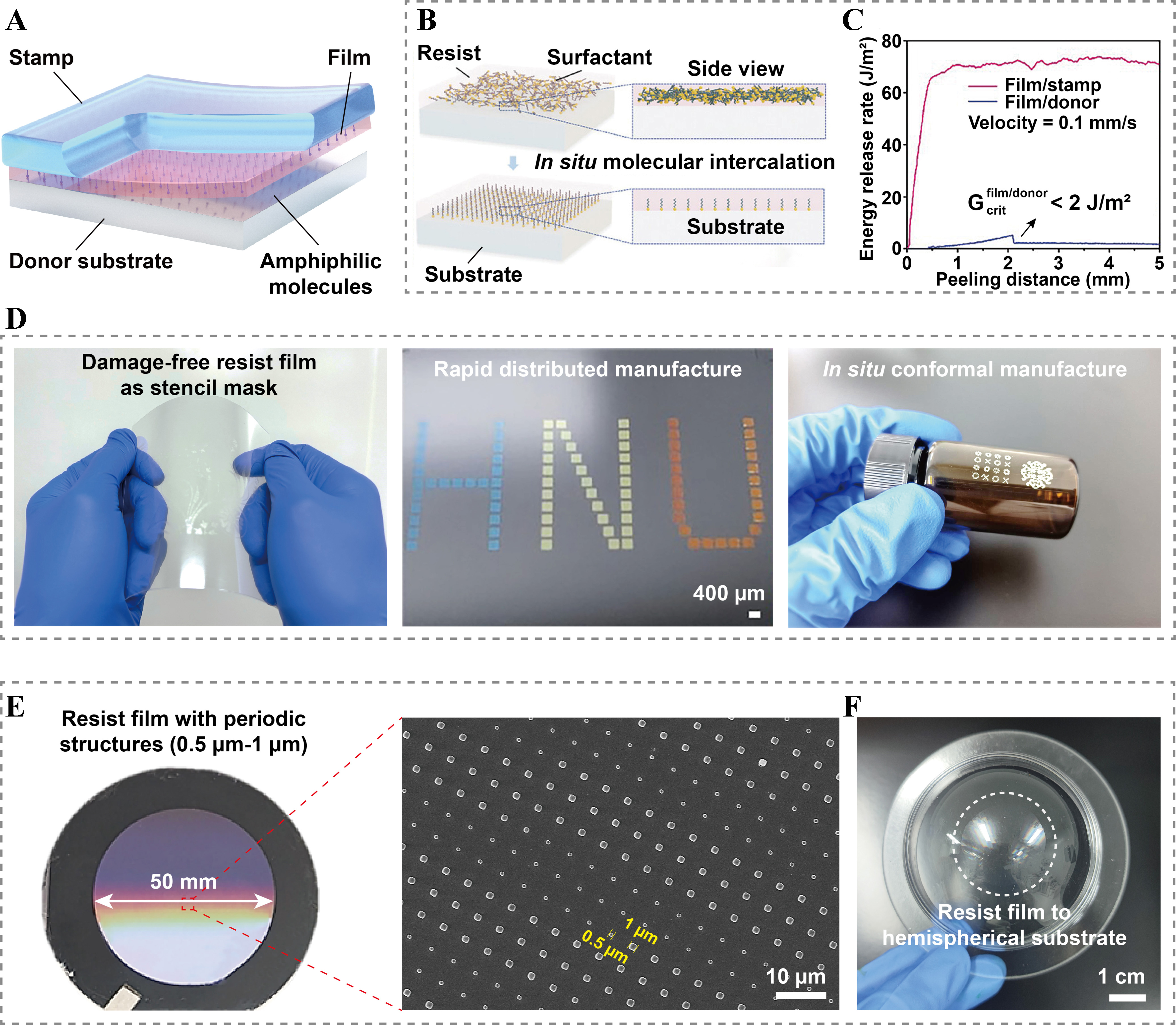
Figure 4. Reducing adhesion at the film/donor interface based on in situ molecular intercalation methods for damage-free transfer printing of fragile resist films. (A) Schematic illustration showing the dry pickup process enabled by in situ incorporation of amphiphilic molecules into the resist matrix; (B) Illustrations of the intercalation mechanism in in situ molecular intercalated resists; (C) Energy release rate of the film/stamp interface and film/donor interface; (D) Distributed and conformal manufacturing based on in situ molecular intercalated resists. Reproduced with permission[43]. Copyright 2024, Wiley-VCH; (E) The 50 mm resist films with the metalens pattern fabricated by PCCL; (F) The capability for damage-free transfer printing of resist films to the hemispherical substrate. Reproduced with permission[74]. Copyright 2025, IOP Publishing. PCCL: Perfect conformal contact lithography.
Building upon this design principle, Chen et al. presented a series of mechanically peelable photoresists via in situ molecular intercalation, including i-line positive modified photoresists and i-line negative modified photoresists[43,73,75], that create a near-zero-adhesion interface (
Recently, Zhou et al. reported perfect conformal contact lithography (PCCL) based on in situ molecular intercalation methods[74]. By exploiting a near-zero-adhesion interface, the photoresist films were peeled off and brought into conformal, zero-gap contact with the mask, enabling wafer-level patterning at the diffraction limit. This technique provides a cost-effective, high-resolution route to large area, stitch-free micro/nanostructures [Figure 4E] and conformal manufacturing [Figure 4F], offering great potential for high-volume production.
In situ molecular intercalation represents an innovative method to achieve near-zero adhesion at the film/donor interface. For photoresists, careful tuning of substrate surface wettability is critical for film formation and uniformity. By circumventing the limitations of SAMs, in situ molecular intercalation methods enable spin-coating onto pre-modified substrates while controlling adhesion through the self-aggregation of amphiphilic molecules at the resist surface. However, this method is currently limited by the range of compatible resists. Extending it to additional systems, such as electron-beam and nanoimprint resists, would broaden its applicability to complex fabrication scenarios inaccessible to traditional lithographic techniques.
Buffer layer-assisted methods
In traditional metal deposition on semiconductor surfaces (e.g., Si, SiO2), metal films can form strong chemical bonds with the substrate. This is true for high-adhesion metals such as platinum (Pt), titanium (Ti), and nickel (Ni), which are crucial for forming metal-semiconductor junctions in electronic and optoelectronic devices[95]. For example, a fuzzy interface is observed between Ti and SiO2 due to atom diffusion and interfacial reaction, resulting in strong adhesion and difficult delamination[96,97]. However, such strong adhesion poses challenges for transfer printing, where peeling stress can damage ultrathin films[98]. Despite SAMs, an alternative approach is to insert a low-adhesion buffer layer at the donor/film interface to achieve a similar reduction in adhesion [Figure 5A]. Liu et al. introduced a graphene buffer layer-assisted method for wafer-scale, damage-free transfer printing of metal films [Figure 5B][44,99]. A single-crystal monolayer of graphene was prepared on germanium and used as the buffer layer. The vdW surface of graphene lacked dangling bonds, resulting in weak interfacial adhesion between the metal and graphene layer, and enabling a 100% transfer printing yield [Figure 5C]. This method allowed metal integration onto diverse substrates, including three-dimensional (3D) materials with dangling bonds and 2D materials free of dangling bonds [Figure 5D][100-102]. In addition, Liu et al. utilized the weak-adhesion metal (e.g., Cu) as the buffer layer to achieve a 100% transfer yield for large-area nanoscale metal films[76]. During pickup, the weak donor/buffer interfacial adhesion allowed the buffer layer and ultrathin film to peel off together. Notably, the buffer layer shifted the mechanical neutral plane of the multilayer peel-off stack, positioning the ultrathin film closer to the neutral plane, thereby reducing in-plane stress and mitigating damage [Figure 5E].
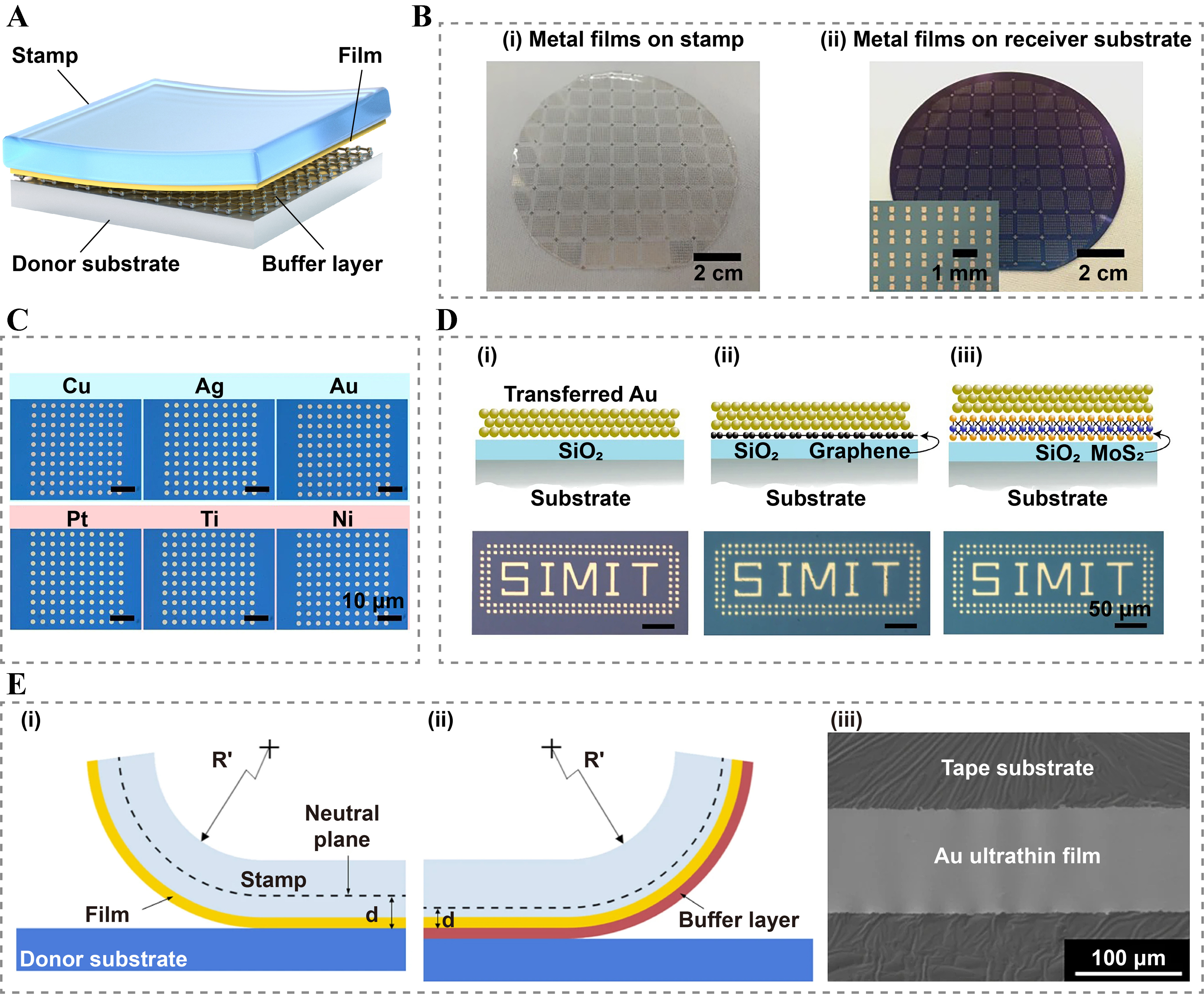
Figure 5. Reducing adhesion at the film/donor interface based on buffer layer-assisted methods for damage-free transfer printing of metal films. (A) Schematic illustration showing the dry pickup process enabled by the prior construction of a buffer layer on the donor substrate; (B) Photographs corresponding to Au patterns transferred onto a 4-inch PVA stamp and printed onto a 4-inch SiO2 wafer; (C) Transfer printing of weakly (Cu, Ag, Au) and strongly (Pt, Ti, Ni) adhering metal films on SiO2 substrate; (D) Au patterns transferred onto different substrates, including SiO2, Gr/SiO2, and MoS2/SiO2. Reproduced with permission[44]. Copyright 2022, Springer Nature; (E) Diagrams of multilayer peel-off sheets without or with a buffer layer, and images of an Au ultrathin film transferred onto a tape with a Cu buffer layer. Reproduced with permission[76]. Copyright 2022, Springer Nature. PVA: Polyvinyl alcohol.
The distinctive surface properties of buffer layers offer substantial potential for damage-free transfer printing. The primary challenge is fabricating defect-free, uniform buffer layers, especially graphene. The synthesis costs and stringent process conditions may also limit broader adoption.
Stress engineering methods
As discussed in the last section, high-adhesion metals such as Pt, Ti, and Ni form strong chemical bonds with substrates during traditional metal deposition processes. While strategies such as SAMs, amphiphilic molecules, or buffer layers can weaken interfacial adhesion, stress engineering methods offer a promising approach to damage-free transfer printing[69,103,104]. For example, Shin et al. introduced a dry transfer printing approach that leverages the interfacial stress to enable damage-free transfer printing of ultrathin films
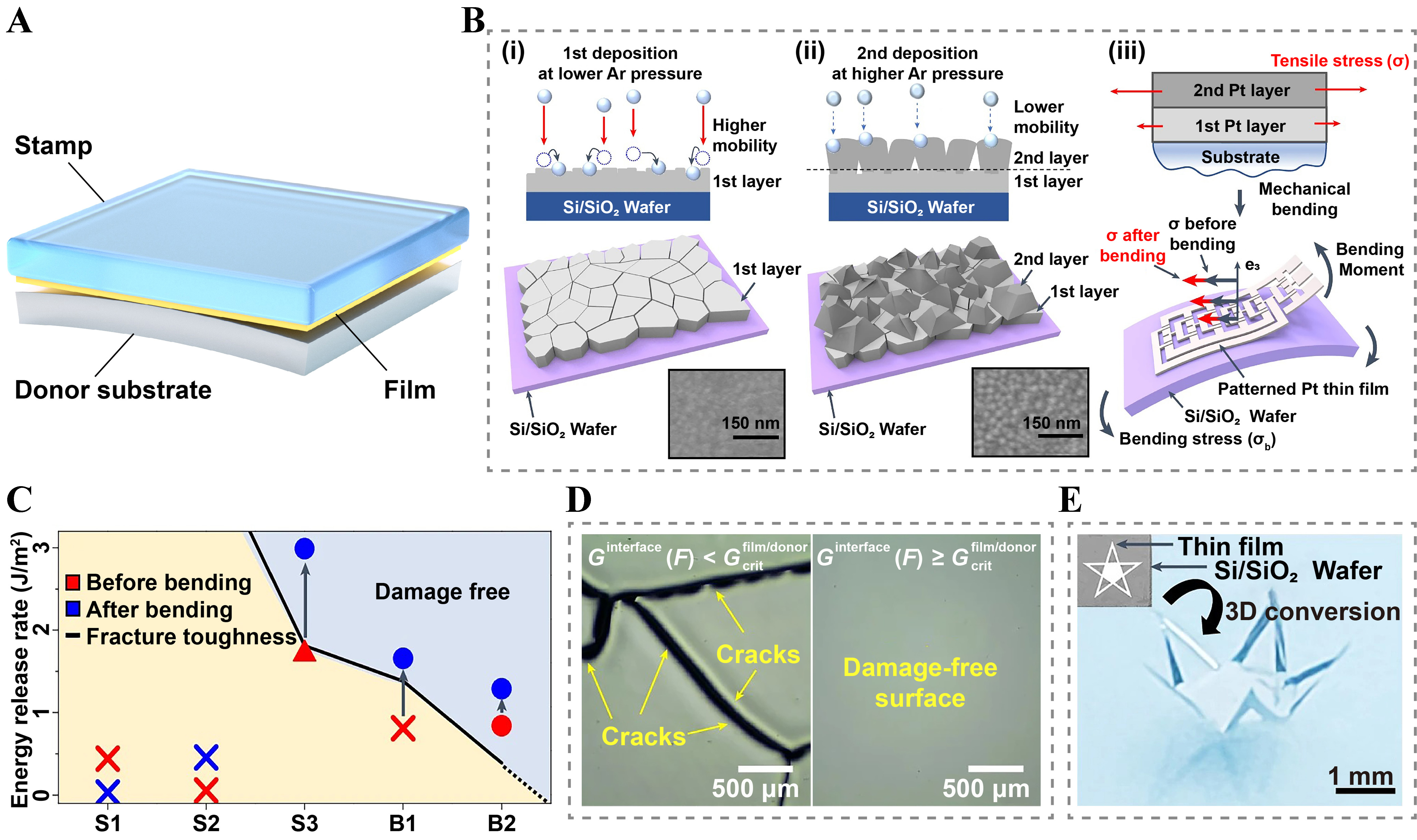
Figure 6. Reducing adhesion at the film/donor interface based on stress engineering methods for damage-free transfer printing of metal films. (A) Schematic illustration showing the dry pickup process enabled by stress engineering; (B) Schematic illustrations describing the formation of single and bilayer-structured Pt thin films and the stress distribution; (C) Comparison of interfacial fracture toughness with strain energy release rates before and after bending; (D) Optical microscope images of cracked and crack-free surfaces of the transferred Pt thin films; (E) Construction of the functional 3D architecture from the 2D thin-film precursor. Reproduced with permission[69]. Copyright 2024, Springer Nature. 3D: Three-dimensional; 2D: two-dimensional.
Stress engineering methods provide a promising approach to preserving the integrity of ultrathin films. However, their compatibility is dependent on the intrinsic material properties of the metal films and substrates, and broader adoption is presently constrained by the narrow range of transferable materials and functional layers.
Regulating adhesion at the film/stamp interface
While reducing adhesion at the film/donor interface is important, the stamp is the cornerstone of transfer printing, governing interfacial adhesion throughout the process. Generally, the adhesion switchability at the film/stamp interface relies on the stamp material’s properties. Traditional elastomeric stamps such as polydimethylsiloxane (PDMS), though widely used, are limited by viscoelasticity: uncontrolled deformation during pickup introduces shear stresses and strain mismatches at the film/stamp interface, leading to microcracks or delamination. For pickup, stronger adhesion at the film/stamp interface is required to drive fracture along the film/donor interface [increasing Ginterface(F)], while the stamp must remain rigid to shield the ultrathin films from in-plane stress [reducing
The summary of different stamps including regulated parameters, adhesion switching ratio, resolution, yield, scalability, and reusability
| Stamp material | Regulated parameter | Adhesion switching ratio | Resolution | Yield | Scalability | Reusability | Ref. |
| Ice | Temperature | Infinite | Nanoscale | 98% | Chip-scale | Not reusable | [78] |
| Liquid metal | Laser | ~224 | Microscale | High | Chip-scale | Reusable | [79] |
| Reflow materials | Temperature | Infinite | Microscale | High | Wafer-scale | Not reusable | [80] |
| TRT | Temperature | Infinite | Microscale | High | Chip-scale | Not reusable | [67] |
| Hydrogel | Wet | > 640 | Microscale | ~100% | Chip-scale | Reusable | [81] |
| SMPs | Temperature | ~150 | Microscale | High | Wafer-scale | Reusable | [32] |
| Phase-change polymers | Temperature | ~1,989 | Nanoscale | 100% | Wafer-scale | Reusable | [66] |
| PDMS (microstructured surface) | Preload | > 1,000 | Microscale | ~100% | Chip-scale | Reusable | [18,54] |
| Ecoflex (balloon shape) | Kinetics | Not mentioned | Microscale | > 99% | Wafer-scale | Reusable | [70] |
Solid-liquid phase-change-assisted methods
In contrast to wet transfer printing, droplet stamps, based on liquid-phase materials (e.g., water, liquid metal), leverage fluidity to mitigate mechanical damage during contact with thin membranes[105,106]. This property enables complete transfer of thin membranes from rigid substrates onto complex 3D geometries[107,108]. Adhesion in droplet stamps arises from Laplace pressure and surface tension, which are weaker than the viscoelastic adhesion of polymeric soft stamps. As a result, droplet stamps are unable to lift high-mass devices, films with complex 3D profiles, or materials exhibiting strong film/substrate interfacial adhesion. These limitations underscore the need for advanced transfer printing techniques that combine reversible adhesion capable of accommodating stress mismatches during contact with robust, on-demand adhesion for pickup and release. Inspired by the low interfacial adhesion of liquid systems, solid-liquid phase-change stamps have been developed to provide strong adhesion in the solid state for pickup and weak adhesion in the liquid state for release [Figure 7A].
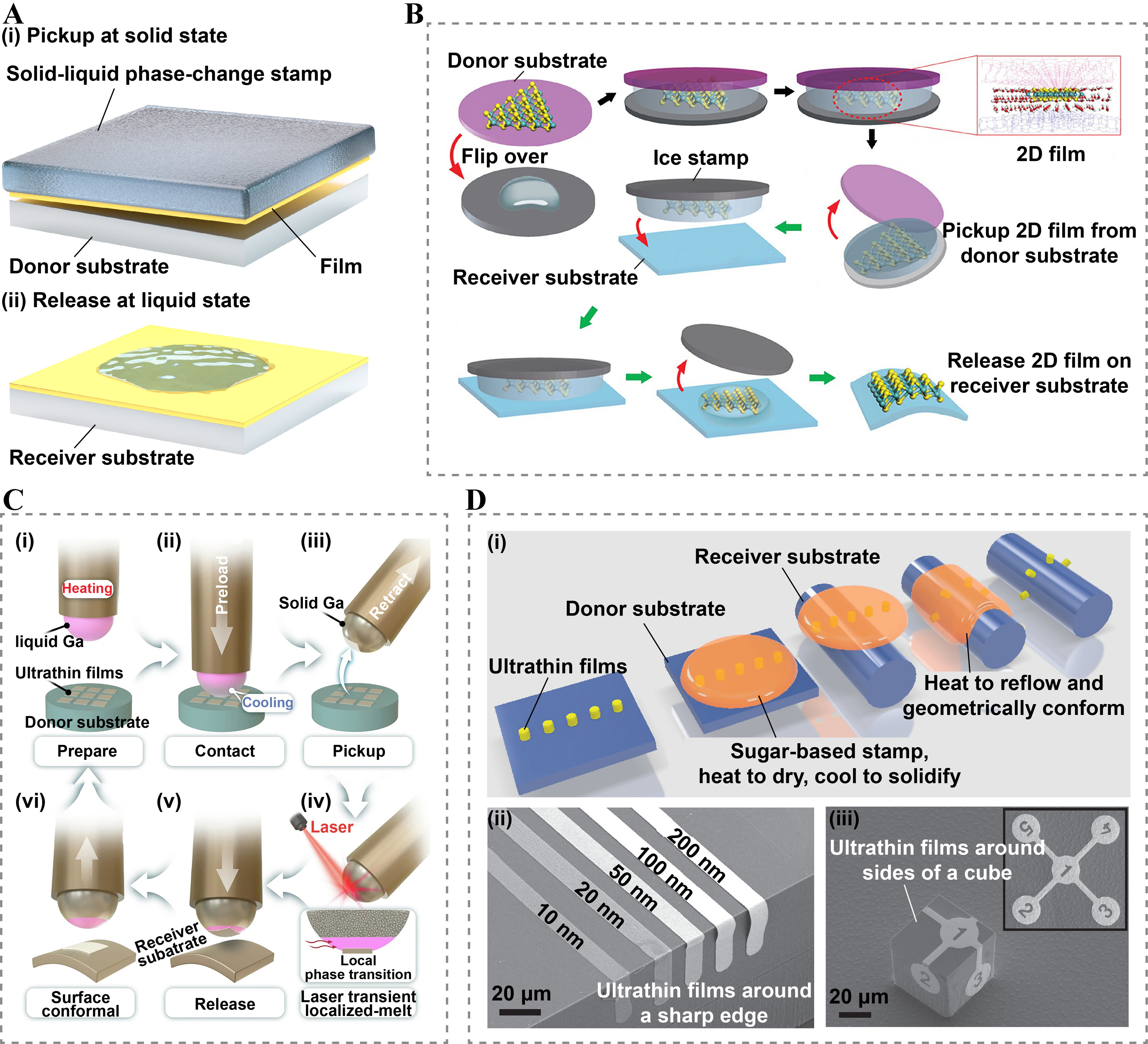
Figure 7. Regulating adhesion at the film/stamp interface based on solid-liquid phase-change-assisted methods for damage-free transfer printing of ultrathin films. (A) Schematic illustration showing the transfer printing process enabled by solid-liquid phase-change-assisted methods; (B) Schematic illustration of the IST for 2D films. Reproduced with permission[78]. Copyright 2023, Wiley-VCH; (C) Schematic illustration of the PLMT for damage-free transfer printing. Reproduced with permission[79]. Copyright 2024, Springer Nature; (D) Schematic illustration of the reflowable transfer for conformal 3D microprinting and SEM images of transfer printing results. Reproduced with permission[80]. Copyright 2022, The American Association for the Advancement of Science. IST: Ice stamp-based transfer printing; 2D: two-dimensional; PLMT: Precision-induced localized molten technique; 3D: three-dimensional; SEM: scanning electron microscope.
Ice stamp-based transfer printing methods
The ice/water system is the simplest among solid-liquid phase-change materials, offering a reversible solid-liquid transition near ambient temperature and residue-free melting[109,110]. For instance, Liu et al. demonstrated an ice stamp-based transfer printing (IST) method for 2D films that avoids damage, residues, and contamination [Figure 7B][78]. In this strategy, thermodynamic control regulated the adhesion of ice. During pickup, adhesion between the 2D films and the ice stamp exceeded the vdW interactions at the film/donor interface under freezing conditions, and the high modulus of ice protected the 2D films from deformation. For release, heating melted the ice stamp to water, weakening interfacial adhesion. The melting step also cleaned the 2D films by dissolving residues, yielding ultra-flat surfaces and long-term stability. Its efficacy was evidenced by the damage-free transfer of MoS2 films to flexible polyethylene terephthalate (PET) substrates with excellent photoelectric performance, attributed to using ice rather than organic solvents, which can damage flexible surfaces[111]. Despite these advantages, IST is constrained to large-scale and high-yield production due to the low dynamic variability of ice adhesion.
Liquid metal stamp-based transfer printing methods
Liquid metals are widely used in stretchable electronics[112]. They also serve as adhesive elements in smart stamp-based transfer printing owing to their highly reversible, switchable adhesion (switching ratio ~200) arising from solid-liquid phase transitions[113]. For example, Shi et al. developed a precision-induced localized molten technique (PLMT) for damage-free transfer printing of ultrathin films, exploiting the fluidity of localized molten liquid metal to prevent damage to ultrathin films while leveraging the high modulus of the solid phase to preserve structural integrity and operational reliability [Figure 7C][79]. For pickup, the liquid metal stamp was cooled to solidify, creating a robust mechanical interlock with the ultrathin films upon contact to strengthen interfacial adhesion. For release, external heating melted the stamp above its melting point, forming a liquid droplet that achieves conformal contact with the ultrathin films under minimal preload. The low-viscosity interface of the molten metal minimized shear stress, approaching a near-zero-adhesion interface. This method offers a simple, efficient, and environmentally unconstrained approach to damage-free transfer printing of ultrathin films. Nevertheless, scalability and the limited range of transferable ultrathin films remain significant challenges.
Reflow materials stamp-based transfer printing methods
While the smart stamps described above enable high-precision transfer printing on flexible substrates, their limited deformability restricts compatibility with complex geometries. To address this, Zabow introduced thermal reflowable materials (e.g., sugar mixtures) as the stamp that enables conformal 3D microprinting with nanoscale precision [Figure 7D][80]. During pickup, the sugar mixture was heated to dehydrate and cooled for solidification at ambient temperature, establishing robust interfacial adhesion in the solid state and protecting ultrathin films from damage. Subsequent viscous thermal flow enabled conformal adhesion over arbitrarily curved surfaces while preserving high-resolution feature registration. Releases were achieved through mechanical delamination or sacrificial layer dissolution[114]. This approach demonstrated damage-free transfer printing of ultrathin films on complex geometries, though challenges in thermal management and patterned-film distortion remain for scalable implementation.
Solid-liquid phase-change-assisted methods provide a versatile, damage-free route for transfer printing of ultrathin films. Unlike traditional elastomeric stamps, solid-liquid phase-change stamps mitigate mechanical degradation, offering a stable strategy for integrating ultrathin films onto arbitrary surfaces. Future work should expand material compatibility and explore dynamic thermal-management schemes to optimize throughput.
Stimuli-responsive-assisted methods
Beyond solid-liquid phase-change-assisted methods, stimuli-responsive-assisted methods enable all-dry, damage-free transfer printing of ultrathin films. These methods employ stimuli-responsive stamps, such as thermal release tape (TRT)[67,68], SMPs[32], and hydrogels[81,115], which dynamically modulate their adhesion properties in response to external triggers. Under ambient conditions, these stamps exhibit strong adhesion and rigidity when picking up ultrathin films. Upon exposure to the specific stimulus (e.g., thermal, optical, hydration, or electrical), the interfacial adhesion drops sharply to release the ultrathin films [Figure 8A]. Therefore, these stimuli-responsive stamps can achieve higher adhesion switching ratios than traditional elastomer stamps.
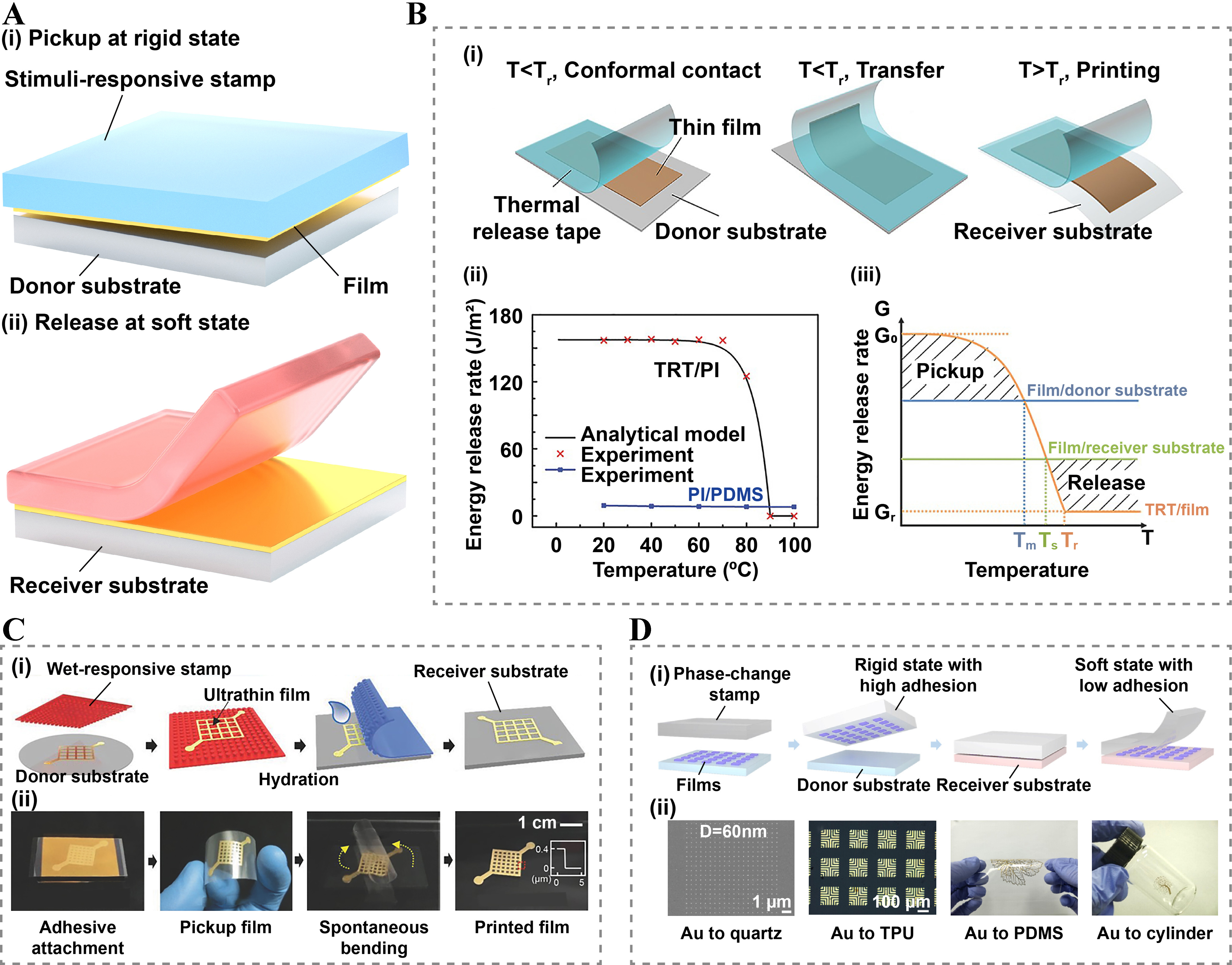
Figure 8. Regulating adhesion at the film/stamp interface based on stimuli-responsive-assisted methods for damage-free transfer printing of ultrathin films. (A) Schematic illustration showing the transfer printing process enabled by stimuli-responsive-assisted methods; (B) Schematic illustration of the thermal release transfer printing method and its principle. Reproduced with permission[67]. Copyright 2017, WILEY-VCH; (C) Schematic illustration and photographs showing the transfer printing process using the wet-responsive stamp. Reproduced with permission[81]. Copyright 2018, WILEY-VCH; (D) Schematic illustration of the transfer printing process using the phase-change stamp and its results. Reproduced with permission[66]. Copyright 2024, American Chemical Society.
TRT stamp-based transfer printing methods
TRT is a widely used stamp in transfer printing, employing temperature-dependent adhesion to enable ultrathin film transfer printing [Figure 8B][67]. Its flexibility facilitates easy operation and conformal contact during printing. Heat modulates the critical energy release rate at the film/stamp interfaces (
Wet-responsive hydrogel stamp-based transfer printing methods
To address this limitation, Yi et al. proposed a reusable, wet-responsive hydrogel stamp for ultrathin film transfer printing [Figure 8C][81]. Composed of poly(ethylene glycol) dimethacrylate (PEGDMA), the reconfigurable stamp absorbed water and underwent dynamic shape adaptation[116]. Cylindrical stem arrays on the stamp surface provided strong adhesion to ultrathin films through vdW interactions. During release, water absorption caused swelling of the stamp, expansion of the stem arrays, and macroscopic bending, enabling damage-free printing. The stamp restored its initial state upon dehydration, demonstrating reusable adhesion switching (switching ratio > 640) for damage-free transfer printing. Its biocompatibility also supports solvent-free, energy-neutral transfers onto biological substrates. A current limitation is that the surface microstructures can restrict the damage-free transfer printing of ultrathin films with high-resolution features.
SMPs stamp-based transfer printing methods
SMPs are a promising class of stimuli-responsive materials for transfer printing stamps due to their capability of deforming into temporary shapes and recovering their original geometry upon external stimulation[117]. Generally, their adhesion and modulus can be tuned dynamically and reversibly, enabling precise control of interfacial interactions. However, their application for damage-free transfer printing of ultrathin films remains challenging because substantial preload forces are often required to achieve conformal contact[118]. To overcome this limitation, Fan et al. proposed an approach for damage-free transfer of metal films for flexible electronics[119]. An SMP resin was spin-coated directly onto the donor substrate and cured in situ to form an interlocked interface with the metal film, ensuring strong adhesion at this boundary. During peel-off, the metal film was embedded in the SMP stamp, whose toughness shielded the ultrathin films from mechanical stress. The SMP served as the final flexible substrate, eliminating a separate transfer-printing step. Despite these advantages, substrate compatibility remains constrained, as the method is not adaptable to diverse target substrates. Recently, Guo et al. reported an SMP-based transfer printing method for photoresist films onto diverse substrates[82]. The stamp exhibited a sharp modulus transition to regulate interfacial adhesion: a high modulus provided strong adhesion and stability during pickup, while a low modulus enabled conformability during release. A current limitation is the requirement for lithography on a PDMS-coated donor, which reduces adhesion at the donor/film interface and thereby restricts the fabrication of high-resolution structures on the donor.
Phase-change polymer stamp-based transfer printing methods
Inspired by the observation that frozen water adheres to substrates and releases upon melting without damage, Chen et al. developed a phase-change polymer stamp for reversible, damage-free transfer printing
Advances in stimuli-responsive materials have produced stamps with higher adhesion switching ratios and faster response times, offering precise on-demand control of interfacial adhesion. However, achieving uniform application of external stimuli across large areas remains challenging, limiting high-volume manufacturing.
Stamp surface engineering methods
For traditional viscoelastic stamps, a fundamental trade-off exists: increasing Young’s modulus helps protect ultrathin films from damage, but it also reduces film/stamp interfacial adhesion, making pick up more difficult. To overcome this challenge, stamp surface engineering methods, including surface energy modification and surface structuring, show promise for damage-free transfer printing of ultrathin films.
Surface energy modification methods
Surface energy (or polarity) of the stamp governs its interfacial adhesion with the film and can be tuned by plasma oxidation, ultraviolet/ozone (UVO) treatment, and related approaches[120-122]. For example, Yoo et al. enhanced adhesion at the film/stamp interface by modulating the PDMS stamp’s surface energy with UVO treatment[123]. A 15 s UVO treatment increased the stamp’s surface modulus from 1.93 to 2.11 MPa, enabling the pickup of ultrathin films with minimal applied pressure (2 kgf·cm-2) while preventing damage to the transferred ultrathin films. This method offers a simple route to enhance the film/stamp interfacial adhesion, and its reversibility and long-term stability could benefit from further exploration.
Surface structuring methods
Structuring of the stamp surface modulates the film/stamp interfacial adhesion by controlling real contact area, stress distribution, and crack propagation paths, enabling directional, reversible, and selective adhesion[124]. For instance, Kim et al. introduced a microstructured elastomeric stamp for deterministic transfer printing that handles multilayer ultrathin-film stacks[18]. Moreover, integrating surface microstructures with stimuli-responsive materials can further enhance film/stamp interfacial adhesion. For example, Lee et al. combined suction-cup microstructures with the stimulus-responsive hydrogel to create a stamp with a high adhesion switching ratio, enabling damage-free transfer printing of ultrathin films onto flexible substrates[26]. While microstructured stamps have shown great promise, their application in damage-free transfer printing of large-area and continuous ultrathin films remains challenging. To address this, Sim et al. reported a conformal additive stamp technology to achieve damage-free transfer printing of continuous ultrathin films onto diverse 3D curvilinear surfaces using a balloon-structured stamp
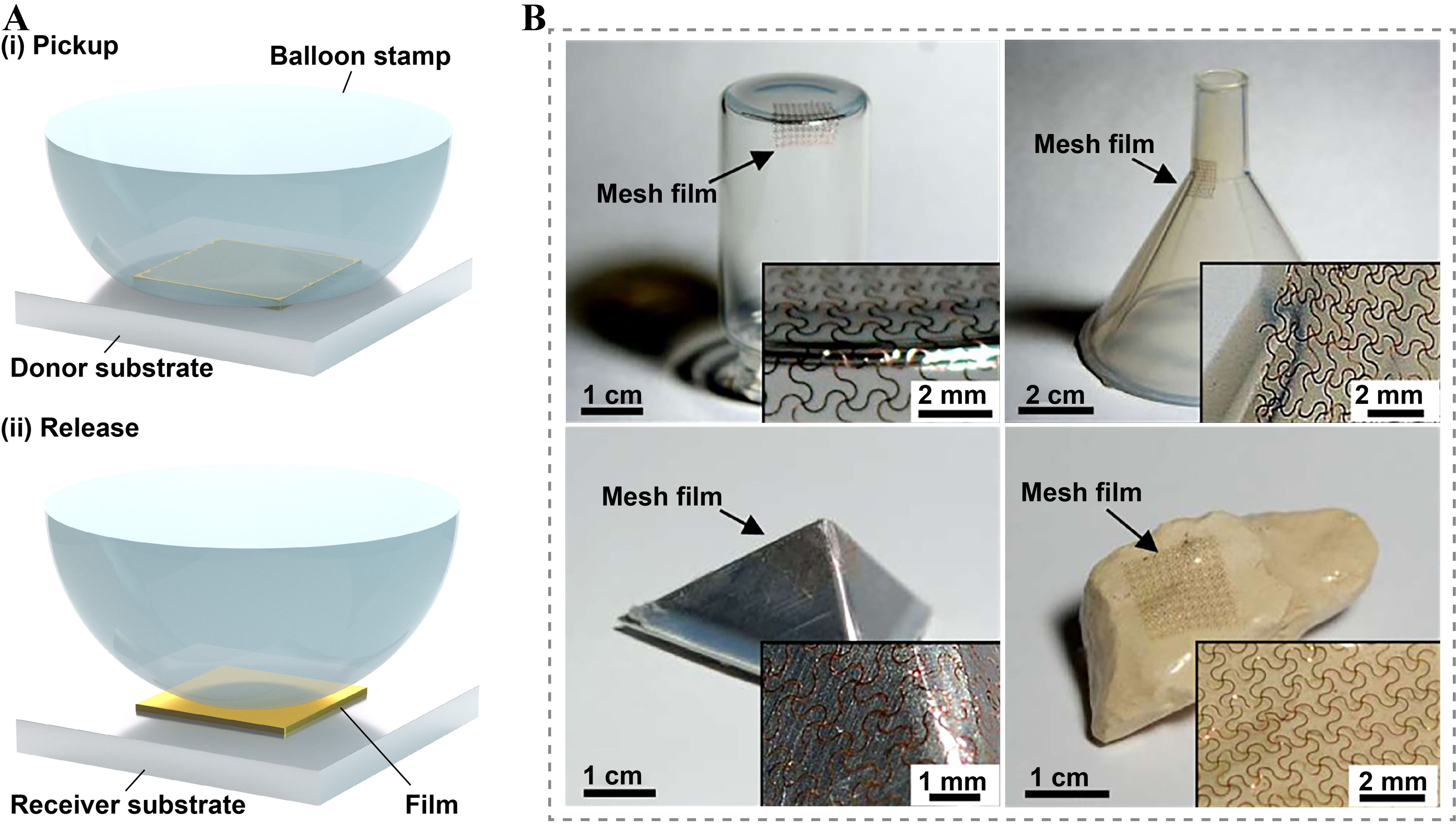
Figure 9. Regulating adhesion at the film/stamp interface based on the conformal additive stamp method for damage-free transfer printing of ultrathin films. (A) Schematic illustration showing the transfer printing process using the balloon stamp; (B) Optical images of the serpentine metal films on various 3D curvilinear substrates, including convex edge, concave edge, pyramid, and uneven surfaces. Reproduced with permission[70]. Copyright 2019, Springer Nature. 3D: Three-dimensional.
Stamp surface engineering enhances interfacial adhesion through designing stamps and offers pathways for dynamic adhesion control. However, achieving damage-free transfer printing of large-area ultrathin films with high-resolution micro/nanostructures remains challenging.
APPLICATIONS
With the increasing diversity of ultrathin films and target substrates, damage-free transfer printing technology has been widely adopted across fields due to its distinct advantages. Beyond uniformity, high resolution, and tunable interfacial adhesion, the ability to preserve the structural and functional integrity of transferred films has attracted substantial interest in advanced applications.
First, continuous and intact metal films produced by damage-free transfer printing exhibit excellent conductivity, enabling use in flexible/curved electronics and 2D films-based electronics. Second, damage-free resist films employed as stencil masks provide remarkable precision for in situ depositing or etching functional materials in flexible/curved electronics. Third, leveraging damage-free transfer printing allows heterogeneous films or devices to be integrated without damage onto unconventional surfaces, such as flexible and curved substrates.
This section discusses applications of damage-free transfer printing for ultrathin films in two domains: in situ manufacturing for flexible/curved electronics and vdW stacking for 2D films-based electronics. We also briefly review additional devices realized via damage-free transfer printing methods to highlight the technology’s adaptability. The robustness, scalability, and substrate versatility of damage-free transfer printing underscore its potential as a transformative platform for next-generation electronics, with opportunities for innovation in multifunctional systems and industrial-scale implementation.
In situ manufacturing for flexible/curved electronics
Photoresist films patterned by lithography on rigid substrates (e.g., Si, SiO2) enable micro/nanostructure fabrication through downstream semiconductor processes such as deposition and etching. However, as applications grow in complexity and diversity, applying these ultrathin films directly to unconventional substrates (e.g., flexible or curved surfaces) remains challenging. Damage-free film transfer printing addresses this limitation by enabling in situ manufacturing on flexible/curved surfaces: patterned resist films are first picked up and then printed intact onto the receiver, while remaining fully compatible with the subsequent semiconductor steps [Figure 10A]. This approach directly delivers damage-free, functional micro/nanostructures on unconventional substrates, highlighting strong potential for flexible/curved electronics.
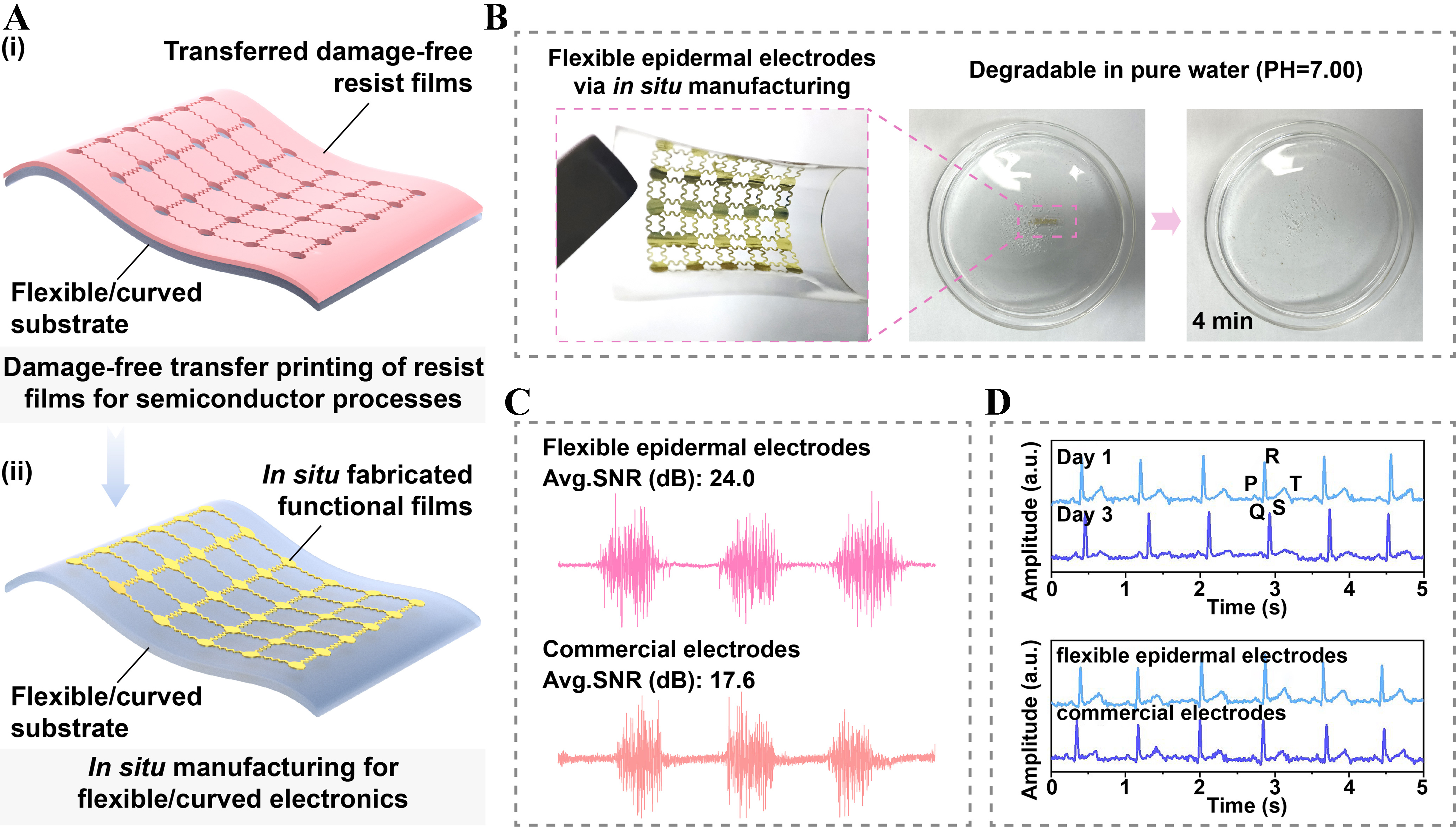
Figure 10. Applications of in situ manufacturing for flexible/curved electronics. (A) Schematic illustration of in situ manufacturing based on transferred damage-free resist films; (B) Optical images showing the flexible epidermal electrodes fabricated via in situ manufacturing, and the degradation of the flexible epidermal electrodes during immersion in pure hot water; (C) EMG signals captured using flexible epidermal electrodes and commercial electrodes. Reproduced with permission[43]. Copyright 2024, Wiley-VCH; (D) ECG signals recorded by flexible epidermal electrodes before and after 3 days, along with a comparison of ECG monitoring between flexible epidermal electrodes and commercial electrodes. Reproduced with permission[66]. Copyright 2024, American Chemical Society. EMG: Electromyograms; ECG: electrocardiograms.
Flexible metal electrodes
A primary application of damage-free transferred ultrathin films is the development of flexible metal electrodes for high-fidelity physiological signal acquisition. Physiological signals such as electroencephalograms (EEG), electrooculograms (EOG), electromyograms (EMG), and electrocardiograms (ECG) serve as biomarkers of neural, muscular, and cardiac activity, yet achieving high spatiotemporal resolution remains difficult with traditional metal electrodes. Metallic materials exhibit a high elastic modulus (> 10 GPa[125]), which hinders conformal contact with soft, curvilinear biological tissues
Curved optoelectronics
The second application of damage-free transferred ultrathin films considered here is the fabrication of curved optoelectronics. 3D curvy curvilinear surfaces are ubiquitous in nature, industry, and biology. By integrating diverse films or devices onto such surfaces, curved electronics enable advances in solar cells, antennas, and soft robotics[70,129,130]. Compared with planar counterparts, curved electronics offer optimized spatial layouts, excellent conformability, and larger integration areas. For example, curved high-density imager arrays provide wide-field, low-aberration imaging with simplified optics[131-133]. However, in traditional transfer printing, physical stacking often yields low interfacial toughness at the film/receiver interface (low Γfilm/receiver), so applied stresses readily induce damage. Damage-free transfer printing of resist films overcomes these limitations by enabling in situ manufacturing of functional micro/nanostructures directly on curved surfaces, enhancing the interface toughness of the deposited material and curved substrates, and offering significant potential for high-performance curved electronics. For instance, Guo et al. fabricated a photodetector array on a curved surface via in situ manufacturing by regulating adhesion at the film/stamp interface[82]. The resulting array exhibited wide-angle sensing by resolving variations in incident light direction across the curved surface. Moreover, Shu et al. realized a nanoscale gold bowtie array on a concave lens by establishing a near-zero-adhesion film/donor interface, showing damage-free fabrication of ultrathin films with nanoscale structures[71].
In summary, damage-free transfer printing bridges advanced material design and flexible/curved electronics applications by eliminating structural defects and enabling mechanically compliant, high-performance devices. As evidenced by flexible electrodes and curved optoelectronics, damage-free transfer printing paves the way for next-generation flexible/curved electronics with high-resolution and high-fidelity micro/nanostructures.
2D films-based electronics
Over the past decade, 2D materials have emerged as a transformative platform for advanced optoelectronics technologies[36,134,135]. While high-yield and high-quality growth of 2D materials by methods (e.g., CVD) is routine, transferring them onto other substrates remains essential for further applications and integration in field-effect transistors (FETs), photodetectors, photovoltaics, and light-emitting devices. However, as-grown 2D films lack dangling bonds, retrieving them requires etching growth substrates, which introduces solvent contamination during transfer[45,46]. Damage-free transfer printing offers a dry route that preserves the structural and electronic integrity of 2D films.
Transferred 2D films for FETs
The FET is a foundational component of electronic systems, enabling logic cells and circuit amplification [Figure 11A]. Continued downscaling of channel lengths below a few nanometers is fundamentally limited by short-channel effects[136]. Notably, 2D materials are promising for advancing complementary metal-oxide-semiconductor (CMOS) technology owing to their atomically smooth surfaces and absence of dangling bonds[137-139]. Crucially, the atomic thickness of a 2D film exhibits immunity to short-channel effects[140,141]. For example, Liu et al. fabricated an ultraclean MoS2 film by regulating adhesion at the film/stamp interface [Figure 11B][78]. MoS2 films transferred onto PET using the IST method exhibited superior uniformity compared with the PMMA-aided transfer (PAT) method. Moreover, the damage-free, contamination-free surface yielded device currents two orders of magnitude higher than those obtained with PAT, a substantial improvement for FET performance.
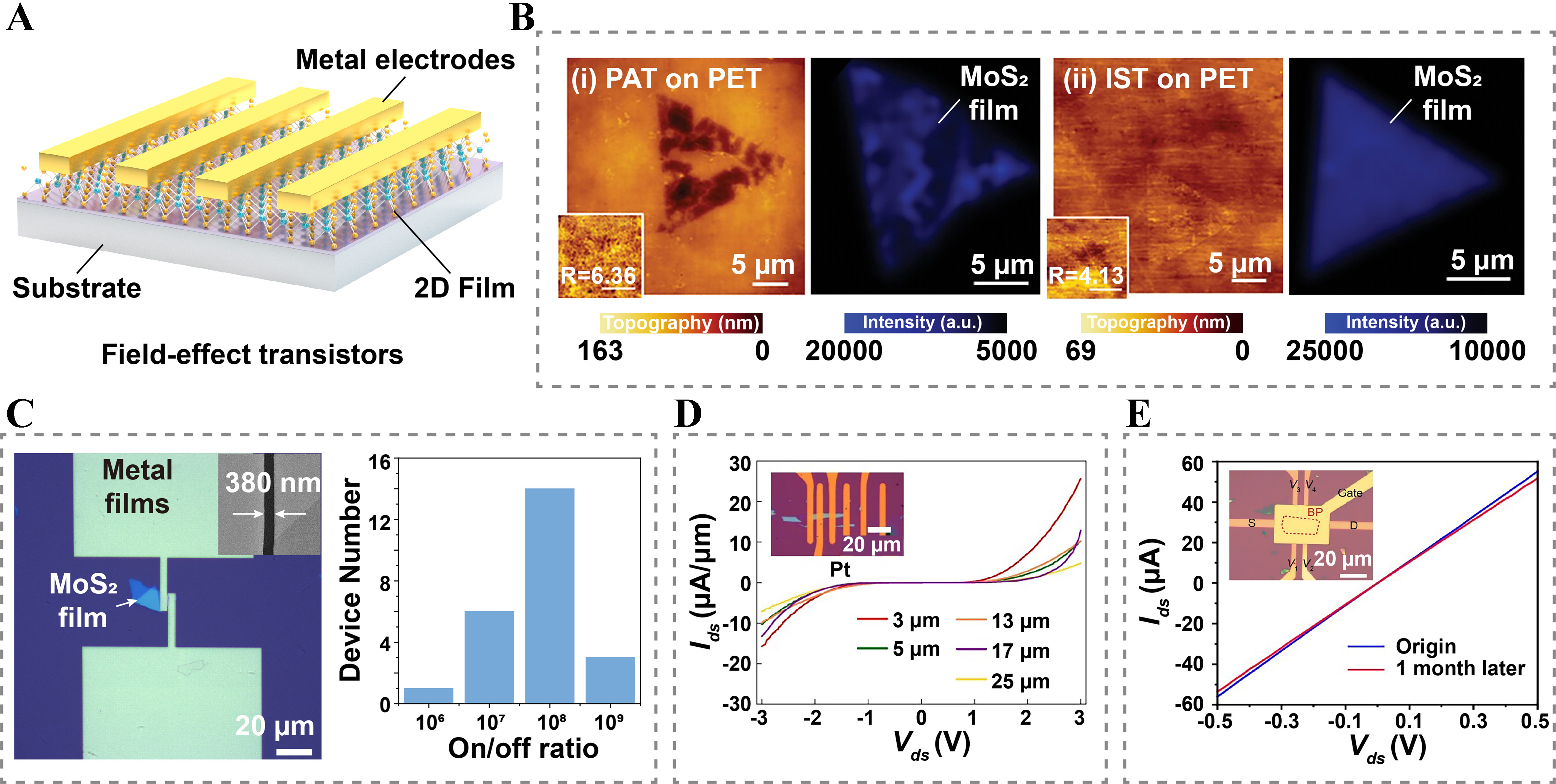
Figure 11. Applications of 2D films-based electronics. (A) Schematic illustration of the FETs; (B) AFM topographic images of MoS2 on PET by PAT and IST, respectively. Reproduced with permission[78]. Copyright 2023, Wiley-VCH; (C) Morphological characterization of the transistor with a channel of 380 nm and its statistical histogram of the ON/OFF ratio of 24 MoS2 transistors with different channel lengths on a SiO2/Si substrate. Reproduced with permission[71]. Copyright 2023, IOP Publishing; (D) Ids-Vds output curves of the MoS2 transistors using transferred Pt electrodes with different channel lengths at back-gate voltage of 60 V. Reproduced with permission[44]. Copyright 2022, Springer Nature; (E) The Ids-Vds curves of the device in the Inset, preserving linear ohmic contact even after exposure to air for one month. Inset: Typical OM image of the fabricated top-gated BP hall-bar device. The dashed line marked out the underlying BP sheet with a thickness of ~11.5 nm. Reproduced with permission[77]. Copyright 2025, Springer Nature. 2D: Two-dimensional; FETs: field-effect transistors; AFM: atomic force microscopy; PET: polyethylene terephthalate; PAT: PMMA-aided transfer; IST: ice stamp-based transfer printing; OM: optical microscope; BP: black phosphorus.
Transferred metal films for FETs
The performance of 2D films-based electronics is critically influenced by metal-2D semiconductor contacts, where minimizing contact resistance remains challenging[142-144]. Traditional metal deposition involving energetic ion bombardment can introduce defects, strain, disorder, and metal diffusion into 2D semiconductors, leading to high-resistance interfaces[44]. By contrast, damage-free transfer printing enables defect-free metal integration. For example, Chen et al. fabricated a MoS2 transistor with Au nanogap electrodes by regulating adhesion at the film/stamp interface[66]. Using the phase-change polymer stamp, damage-free metal electrodes with a 680 nm channel-length were laminated onto a MoS2 flake, achieving an on/off ratio of ~6 × 10⁴. Similarly, Shu et al. realized arrays of MoS2 transistors with in situ Au nanogap electrodes by establishing a near-zero-adhesion interface at the film/donor substrate, enabling high-fidelity transfer of 380 nm channel-length metal electrodes [Figure 11C][71]. The resulting MoS2 transistor exhibited an exceptional on/off ratio of ~108, demonstrating stable, reliable performance for electronic applications. Moreover, Liu et al. demonstrated wafer-scale integration of both ohmic and Schottky contacts in MoS2 transistors by reducing adhesion at the film/donor substrate [Figure 11D][44]. Selective metal transfer onto 2D films produced good contacts: Ag formed ohmic interfaces (linear Ids-Vds characteristics), whereas Cu, Au, and Pt contacts yielded Schottky behavior. Further, He et al. fabricated a top-gated Hall bar of black phosphorus (BP) by reducing adhesion at the film/donor interface [Figure 11E][77]. The device, comprising contact metal (30 nm Au), dielectric (10 nm Al2O3), and top-gated electrode (10 nm Pd and 50 nm Au), was damage-free transferred on the fragile BP layer, avoiding surface degradation and maintaining stable operation for over one month.
Above all, damage-free transfer printing offers a promising solution to critical challenges in 2D films integration. It opens an avenue toward diverse exotic heterostructures and enables higher performance of the 2D films-based electronics.
Other devices
Leveraging damage-free transfer printing of ultrathin films, a variety of devices, including thin-film batteries, thin-film solar cells, sensors, and microscale light-emitting diodes (μ-LEDs), can be transfer-printed onto target substrates without damage. For example, Shin et al. fabricated a flexible Pt/LiCoO2 thin film battery by depositing a stress-engineered Pt bilayer, which enabled the damage-free transfer printing of the device[69]. The fabricated device exhibited a capacity of 16.9 μAh·cm-2 and retained ~97.5% of its initial capacity after 100 charge-discharge cycles, underscoring the electrochemical stability imparted by the damage-free process. Further, Sim et al. demonstrated hemispherical, thin-film solar cells using conformal additive stamp printing[70]. The damage-free, hemispherical devices showed distinct advantages in wide-angle light harvesting compared with traditional planar devices[129,145]. Additionally, Wang et al. achieved programmable, damage-free transfer printing of heterogeneous device arrays, including strain sensors, surface acoustic wave sensors, and μ-LEDs, onto flexible substrates by regulating adhesion at the film/stamp interface using TRT[68]. Combined with laser-assisted patterning, this approach enabled high-throughput, cost-effective integration of multifunctional systems.
CHALLENGES AND PERSPECTIVES
Ultrathin films are the fundamental functional elements of advanced devices. Therefore, industrial-scale fabrication of damage-free ultrathin films will influence innovation in integrated circuits, flexible electronics, curved electronics, and 2D materials. Despite substantial progress in advanced damage-free transfer printing technologies, which can produce wafer-scale ultrathin films with high yield and high-resolution patterns, several challenges remain. In this section, challenges and potential solutions will be discussed, as well as prospects for extending these technologies to industrial-scale manufacturing.
First, achieving both macroscale area and nanoscale thickness remains difficult for damage-free transfer printing of ultrathin films, limiting yield and throughput in industrial applications. On the one hand, the interfacial energy release rate follows Ginterface(F) = F/w, where F is the peel force and w is the width (out-of-plane direction)[2]. This formula indicates that larger peel areas (i.e., increased w) require higher F to satisfy Ginterface(F) ≥
Second, on-demand reversible interfacial adhesion is still a research focus. Though existing smart stamps exhibit adhesion switchability, it remains a challenge to achieve damage-free transfer printing of ultrathin films with high-density nanoscale structures, because current systems rarely provide both near-zero weak adhesion and robust strong adhesion simultaneously. Moreover, adhesion switching triggered by external stimuli can induce internal stresses within the stamp, necessitating designs that balance high adhesion contrast with low transition-induced stress. Integrating smart materials with engineered nanostructures to achieve a larger adhesion switching ratio and faster responsibility may offer a general route toward universal, damage-free transfer printing. Thus, developing high-performance, reusable smart stamps is necessary in industrial manufacturing.
Third, strain-induced stress remains challenging for damage-free transfer printing of ultrathin films onto unconventional substrates. Transferring films onto 3D curved surfaces, whether developable surfaces (zero Gaussian curvature) or non-developable surfaces (non-zero Gaussian curvature), often requires stretching, compressing, or tearing of both the stamp and the ultrathin film to achieve conformity, unavoidably introducing stresses that can cause film fracture, cracking, or delamination[149]. Such damage critically compromises the electrical and mechanical performance of curved electronics. Some solutions have been reported, such as reducing the film thickness to improve flexibility[149], which demands stamps with high stretchability and low modulus for conformal contact on complex 3D topographies. In addition, developing stretchable functional films with increased interfacial toughness Γfilm/receiver provides a pathway to mitigate strain-induced damage.
Above all, to transition from the laboratory demonstrations to industrial-scale manufacturing, the two damage-free dry transfer printing strategies discussed in this review must be implemented simultaneously. Reducing adhesion at the film/donor interface to near-zero is a foundational requirement throughout the transfer printing. A near-zero-adhesion interface can enable ~100% pickup yield and offers the potential for large-area (meter scale) transfer. Regulating adhesion at the film/stamp interface is equally crucial, as the stamp is the intermediate carrier that determines the final yield of transfer-printed ultrathin films. Advancing stamp materials to improve environmental stability, long-term reliability, reusability, and compatibility with roll-to-plate or roll-to-roll processes will enhance efficiency and scalability. In addition, strengthening adhesion at the receiver substrate can improve yield. Moreover, progress in enabling methodologies, such as achieving perfect conformal contact and high-precision alignment, will be coupled to advances in damage-free dry transfer printing. As these foundational technologies mature, damage-free dry transfer printing will be better positioned for industrial adoption.
CONCLUSION
This review focuses on the cutting-edge methods for damage-free dry transfer printing of ultrathin films, particularly interfacial adhesion engineering principles that enable on-demand modulation of adhesion strengths under ultralow peeling stress. Two classes of strategies, including reducing adhesion at the film/donor interface and regulating adhesion at the film/stamp interface, were introduced in the “Introduction” section. In detail, we describe surface modification, in situ molecular intercalation, buffer layer-assisted, and stress engineering methods to reduce adhesion at the film/donor interface. We also outline solid-liquid phase-change-assisted, stimuli-responsive-assisted methods, and stamp surface engineering methods have been introduced to regulate adhesion at the film/stamp interface. An overview of these damage-free transfer-printing methodologies is provided in Figure 2, with detailed comparative analyses in Tables 1 and 2. In addition, transformative applications of these techniques in emerging fields, including flexible/curved electronics and 2D film-based electronics, are discussed in the “Strategies and principles” section. Finally, challenges and perspectives on current damage-free transfer printing technologies are considered in the “Challenges and perspectives” section.
As advanced devices impose stricter requirements on the quality, thickness, scalability, and applicable substrates of ultrathin films, traditional film fabrication and transfer printing techniques are insufficient. Building on traditional approaches, damage-free transfer printing offers precise control of interfacial adhesion, such as constructing near-zero-adhesion film/donor interfaces and developing smart stamps with a higher adhesion switching ratio. Though current damage-free transfer printing methods have demonstrated wafer-scale capability with high resolution, significant challenges remain for their transition to industrial-scale manufacturing. Future research should expand in two directions: (1) improving yield and process stability for larger-area and thinner ultrathin films; and (2) advancing enabling methodologies, such as achieving perfect conformal contact and high-precision alignment. With continued progress, damage-free transfer printing is poised to mature into a scalable, high-fidelity platform for fabricating ultrathin films and next-generation devices on arbitrary substrates.
DECLARATIONS
Authors’ contributions
Conceptualization and supervision: Chen, L.; Duan, H.
Investigation, original draft, and figure editing: Fan, F.; Wang, Y.; Wang, P.; Niu, Y.; Lv, Y.; Liu, P.
Manuscript revision: Fan, F.; Chen, L.; Shu, Z.; Zhou, Y.; Dong, W.; Zhang, N.; Li, C.; Duan, H.
Project administration: Shu, Z.; Duan, H.
Availability of data and materials
Not applicable.
Financial support and sponsorship
This work was supported by the National Key Research and Development Program of China (2022YFB4602600), the National Natural Science Foundation of China (52425508, 52221001), and the Hunan Provincial Natural Science Foundation of China (2025JJ60286).
Conflicts of interest
Zhang, N. and Li, C were employed by the company Hunan Initial New Materials Co., Ltd. All authors declared that there are no conflicts of interest.
Ethical approval and consent to participate
Not applicable.
Consent for publication
Not applicable.
Copyright
© The Author(s) 2025.
REFERENCES
1. Meitl, M. A.; Zhu, Z.; Kumar, V.; et al. Transfer printing by kinetic control of adhesion to an elastomeric stamp. Nature. Mater. 2006, 5, 33-8.
2. Feng, X.; Meitl, M. A.; Bowen, A. M.; Huang, Y.; Nuzzo, R. G.; Rogers, J. A. Competing fracture in kinetically controlled transfer printing. Langmuir 2007, 23, 12555-60.
3. Kim, S. S.; Chalykh, R.; Kim, H.; et al. Progress in EUV lithography toward manufacturing. In Proceedings of SPIE - The International Society for Optical Engineering, San Jose, USA. February 27 - March 02, 2017. SPIE: 2017. Vol. 10143, pp. 1014306. https://www.researchgate.net/publication/315650357_Progress_in_EUV_lithography_toward_manufacturing. (accessed 11 Sep 2025).
4. Cheimarios, N.; Kokkoris, G.; Boudouvis, A. G. Multiscale modeling in chemical vapor deposition processes: models and methodologies. Arch. Computat. Methods. Eng. 2021, 28, 637-72.
5. Luo, H.; Li, C.; Wang, S.; Zhang, S.; Song, J. Switchable adhesive based on shape memory polymer with micropillars of different heights for laser-driven noncontact transfer printing. ACS. Appl. Mater. Interfaces. 2024, 16, 9443-52.
6. Zhang, S.; Luo, H.; Wang, S.; et al. A thermal actuated switchable dry adhesive with high reversibility for transfer printing. Int. J. Extrem. Manuf. 2021, 3, 035103.
7. Chen, F.; Gai, M.; Sun, N.; et al. Laser-driven hierarchical “gas-needles” for programmable and high-precision proximity transfer printing of microchips. Sci. Adv. 2023, 9, eadk0244.
8. Chen, F.; Bian, J.; Hu, J.; et al. Mass transfer techniques for large-scale and high-density microLED arrays. Int. J. Extrem. Manuf. 2022, 4, 042005.
9. Wang, Y.; Solberg, S.; Lu, J.; et al. Programmable micro-transfer-printing for heterogeneous material integration. AIP. Adv. 2022, 12, 065110.
10. Linghu, C.; Zhang, S.; Wang, C.; Song, J. Transfer printing techniques for flexible and stretchable inorganic electronics. npj. Flex. Electron. 2018, 2, 26.
11. Zhou, H.; Qin, W.; Yu, Q.; Cheng, H.; Yu, X.; Wu, H. Transfer printing and its applications in flexible electronic devices. Nanomaterials 2019, 9, 283.
12. Kim, Y.; Yang, J.; Choi, M. K. Recent advances in transfer printing of colloidal quantum dots for high-resolution full color displays. Korean. J. Chem. Eng. 2024, 41, 3469-82.
13. Yoon, J.; Lee, S.; Kang, D.; Meitl, M. A.; Bower, C. A.; Rogers, J. A. Heterogeneously integrated optoelectronic devices enabled by micro-transfer printing. Adv. Opt. Mater. 2015, 3, 1313-35.
14. Huang, Z.; Lin, Y. Transfer printing technologies for soft electronics. Nanoscale 2022, 14, 16749-60.
15. Cheng, H.; Li, M.; Wu, J.; et al. A viscoelastic model for the rate effect in transfer printing. J. Appl. Mech. 2013, 80, 041019.
16. Yin, H.; Ma, Y.; Feng, X. Rate-dependent peeling behavior of the viscoelastic film-substrate system. Int. J. Solids. Struct. 2024, 286-7, 112588.
17. Keum, H.; Carlson, A.; Eisenhaure, J. D.; Rogers, J. A.; Kim, S. Deterministically assembled three-dimensional silicon microstructures using elastomeric stamps. In 2012 IEEE 25th International Conference on Micro Electro Mechanical Systems (MEMS), Paris, France. January 29 - February 02, 2012. IEEE; 2012. pp. 224-7.
18. Kim, S.; Wu, J.; Carlson, A.; et al. Microstructured elastomeric surfaces with reversible adhesion and examples of their use in deterministic assembly by transfer printing. Proc. Natl. Acad. Sci. U. S. A. 2010, 107, 17095-100.
19. Zhao, X.; Liang, Z.; Zhang, R.; Zhao, Q.; Ma, Y.; Feng, X. Dual-interface competitive fracture model for curvature-based transfer printing method. Adv. Mater. Interfaces. 2024, 11, 2400303.
20. Cho, S.; Kim, N.; Song, K.; Lee, J. Adhesiveless transfer printing of ultrathin microscale semiconductor materials by controlling the bending radius of an elastomeric stamp. Langmuir 2016, 32, 7951-7.
21. Carlson, A.; Kim-Lee, H.; Wu, J.; et al. Shear-enhanced adhesiveless transfer printing for use in deterministic materials assembly. Appl. Phys. Lett. 2011, 98, 264104.
22. Yang, S. Y.; Carlson, A.; Cheng, H.; et al. Elastomer surfaces with directionally dependent adhesion strength and their use in transfer printing with continuous roll-to-roll applications. Adv. Mater. 2012, 24, 2117-22.
23. Lee, J.; So, H. Aphid-inspired and thermally-actuated soft gripper using 3D printing technology. Macromol. Rapid. Commun. 2023, 44, e2300352.
24. Linghu, C.; Wang, C.; Cen, N.; Wu, J.; Lai, Z.; Song, J. Rapidly tunable and highly reversible bio-inspired dry adhesion for transfer printing in air and a vacuum. Soft. Matter. 2018, 15, 30-7.
25. Liang, C.; Wang, F.; Huo, Z.; Shi, B.; Tian, Y.; Zhang, D. Adhesion performance study of a novel microstructured stamp for micro-transfer printing. Soft. Matter. 2021, 17, 4989-97.
26. Lee, H.; Um, D. S.; Lee, Y.; Lim, S.; Kim, H. J.; Ko, H. Octopus-inspired smart adhesive pads for transfer printing of semiconducting nanomembranes. Adv. Mater. 2016, 28, 7457-65.
27. Yoo, J. I.; Kim, S. H.; Ko, H. C. Stick-and-play system based on interfacial adhesion control enhanced by micro/nanostructures. Nano. Res. 2021, 14, 3143-58.
28. Shi, X.; Yang, L.; Li, S.; Guo, Y.; Zhao, Z. Magnetic-field-driven switchable adhesion of NdFeB/PDMS composite with gecko-like surface. Nano. Res. 2023, 16, 6840-8.
29. Saeidpourazar, R.; Li, R.; Li, Y.; et al. Laser-driven micro transfer placement of prefabricated microstructures. J. Microelectromech. Syst. 2012, 21, 1049-58.
30. Huang, Y.; Zheng, N.; Cheng, Z.; et al. Direct laser writing-based programmable transfer printing via bioinspired shape memory reversible adhesive. ACS. Appl. Mater. Interfaces. 2016, 8, 35628-33.
31. Luo, H.; Wang, C.; Linghu, C.; Yu, K.; Wang, C.; Song, J. Laser-driven programmable non-contact transfer printing of objects onto arbitrary receivers via an active elastomeric microstructured stamp. Natl. Sci. Rev. 2020, 7, 296-304.
32. Linghu, C.; Zhang, S.; Wang, C.; et al. Universal SMP gripper with massive and selective capabilities for multiscaled, arbitrarily shaped objects. Sci. Adv. 2020, 6, eaay5120.
33. Eisenhaure, J.; Kim, S. Laser-driven shape memory effect for transfer printing combining parallelism with individual object control. Adv. Mater. Technol. 2016, 1, 1600098.
34. Kim, J.; Kim, S.; Yun, T.; et al. Shape memory polymer surfaces with controllable roughness for multiscale switchable dry adhesion. Nat. Commun. 2025, 16, 4954.
35. Gablech, I.; Głowacki, E. D. State-of-the-art electronic materials for thin films in bioelectronics. Adv. Elect. Mater. 2023, 9, 2300258.
36. Pham, P. V.; Mai, T. H.; Dash, S. P.; et al. Transfer of 2D films: from imperfection to perfection. ACS. Nano. 2024, 18, 14841-76.
37. Nam, Y.; Shin, D.; Choi, J. G.; et al. Ultra-thin GaAs single-junction solar cells for self-powered skin-compatible electrocardiogram sensors. Small. Methods. 2024, 8, e2301735.
38. Han, S.; Xu, Z.; Meng, Y.; Bae, S. Chapter 17 - 2D materials–based electronics enabled by transfer printing technologies. In Transfer printing technologies and applications. Elsevier; 2024. pp. 475-93.
39. Sakthinathan, S.; Meenakshi, G. A.; Vinothini, S.; et al. A review of thin-film growth, properties, applications, and future prospects. Processes 2025, 13, 587.
40. Malureanu, R.; Lavrinenko, A. Ultra-thin films for plasmonics: a technology overview. Nanotechnol. Rev. 2015, 4, 259-75.
41. Gao, W.; Huang, J.; He, J.; et al. Recent advances in ultrathin materials and their applications in e-skin. InfoMat 2023, 5, e12426.
42. Huang, W.; Ong, X. C.; Kwon, I. S.; et al. Ultracompliant hydrogel-based neural interfaces fabricated by aqueous-phase microtransfer printing. Adv. Funct. Mater. 2018, 28, 1801059.
43. Chen, L.; Liang, H.; Liu, P.; et al. Sustainable lithography paradigm enabled by mechanically peelable resists. Adv. Mater. 2025, 37, e2410978.
44. Liu, G.; Tian, Z.; Yang, Z.; et al. Graphene-assisted metal transfer printing for wafer-scale integration of metal electrodes and two-dimensional materials. Nat. Electron. 2022, 5, 275-80.
45. Bae, S.; Kim, H.; Lee, Y.; et al. Roll-to-roll production of 30-inch graphene films for transparent electrodes. Nat. Nanotechnol. 2010, 5, 574-8.
46. Zhang, X.; Zhou, L.; Wang, S.; et al. Se-mediated dry transfer of wafer-scale 2D semiconductors for advanced electronics. Nat. Commun. 2025, 16, 4468.
47. Gong, Z. Layer-scale and chip-scale transfer techniques for functional devices and systems: a review. Nanomaterials 2021, 11, 842.
48. Wu, H.; Sariola, V.; Zhu, C.; Zhao, J.; Sitti, M.; Bettinger, C. J. Transfer printing of metallic microstructures on adhesion-promoting hydrogel substrates. Adv. Mater. 2015, 27, 3398-404.
49. Le Borgne, B.; De Sagazan, O.; Crand, S.; Jacques, E.; Harnois, M. Conformal electronics wrapped around daily life objects using an original method: water transfer printing. ACS. Appl. Mater. Interfaces. 2017, 9, 29424-9.
50. Le Borgne, B.; Liu, S.; Morvan, X.; et al. Water transfer printing enhanced by water-induced pattern expansion: toward large-area 3D electronics. Adv. Mater. Technol. 2019, 4, 1800600.
51. Sun, W.; Li, Z.; Zhu, X.; et al. Electric field-driven jetting and water-assisted transfer printing for high-resolution electronics on complex curved surfaces. Electronics 2024, 13, 1182.
52. Xu, Z.; Guo, Q.; Yang, L.; et al. Water-soluble and environmentally friendly UV photodetector fabricated through solvent-free material patterning. In 2025 IEEE 38th International Conference on Micro Electro Mechanical Systems (MEMS), Kaohsiung, Taiwan. January 19-23, 2025. IEEE; 2025. pp. 708-11.
53. Anderson, T. L. Fracture mechanics: fundamentals and applications. 3rd edition. CRC press; 2005.
54. Hutchinson, J. W.; Suo, Z. Mixed mode cracking in layered materials. Adv. Appl. Mech. 1991, 29, 63-191.
55. León Baldelli, A.; Babadjian, J.; Bourdin, B.; Henao, D.; Maurini, C. A variational model for fracture and debonding of thin films under in-plane loadings. J. Mech. Phys. Solids. 2014, 70, 320-48.
56. Jung, A.; Ha, N.; Kim, N.; et al. Multiple transfer of layer-by-layer nanofunctional films by adhesion controls. ACS. Appl. Mater. Interfaces. 2019, 11, 48476-86.
57. Li, Y.; Zhang, F.; Wang, S. Regulatable interfacial adhesion between stamp and ink for transfer printing. Interdiscip. Mater. 2024, 3, 29-53.
58. Chen, Z.; Zhang, C.; Zheng, Z. Advancements in transfer printing techniques for flexible electronics: adjusting interfaces and promoting versatility. Int. J. Extrem. Manuf. 2024, 6, 052005.
59. Ahn, J.; Jang, H.; Jeong, Y.; et al. Illuminating recent progress in nanotransfer printing: core principles, emerging applications, and future perspectives. Adv. Sci. 2024, 11, e2303704.
60. Linghu, C.; Mu, T.; Zhao, W.; et al. Advancing smart dry adhesives with shape memory polymers. Int. J. Smart. Nano. Mater. 2025, 16, 103-43.
61. Zhang, L.; Zhang, C.; Tan, Z.; Tang, J.; Yao, C.; Hao, B. Research progress of microtransfer printing technology for flexible electronic integrated manufacturing. Micromachines 2021, 12, 1358.
62. Wu, H.; Tian, Y.; Luo, H.; Zhu, H.; Duan, Y.; Huang, Y. Fabrication techniques for curved electronics on arbitrary surfaces. Adv. Mater. Technol. 2020, 5, 2000093.
63. Park, J.; Lee, Y.; Lee, H.; Ko, H. Transfer printing of electronic functions on arbitrary complex surfaces. ACS. Nano. 2020, 14, 12-20.
64. Zeng, Y.; Peng, C.; Hong, W.; et al. Review on metallization approaches for high-efficiency silicon heterojunction solar cells. Trans. Tianjin. Univ. 2022, 28, 358-73.
65. Lee, C. H.; Kim, D. R.; Zheng, X. Transfer printing methods for flexible thin film solar cells: basic concepts and working principles. ACS. Nano. 2014, 8, 8746-56.
66. Chen, L.; Liang, H.; Liu, P.; et al. Phase-change stamp with highly switchable adhesion and stiffness for damage-free multiscale transfer printing. ACS. Nano. 2024, 18, 23968-78.
67. Yan, Z.; Pan, T.; Xue, M.; et al. Thermal release transfer printing for stretchable conformal bioelectronics. Adv. Sci. 2017, 4, 1700251.
68. Wang, C.; Linghu, C.; Nie, S.; et al. Programmable and scalable transfer printing with high reliability and efficiency for flexible inorganic electronics. Sci. Adv. 2020, 6, eabb2393.
69. Shin, Y.; Hong, S.; Hur, Y. C.; et al. Damage-free dry transfer method using stress engineering for high-performance flexible two- and three-dimensional electronics. Nat. Mater. 2024, 23, 1411-20.
70. Sim, K.; Chen, S.; Li, Z.; et al. Three-dimensional curvy electronics created using conformal additive stamp printing. Nat. Electron. 2019, 2, 471-9.
71. Shu, Z.; Feng, B.; Liu, P.; et al. Near-zero-adhesion-enabled intact wafer-scale resist-transfer printing for high-fidelity nanofabrication on arbitrary substrates. Int. J. Extrem. Manuf. 2024, 6, 015102.
72. Chen, Z.; Lu, X.; Wang, H.; et al. Electrochemical replication and transfer for low-cost, sub-100 nm patterning of materials on flexible substrates. Adv. Mater. 2023, 35, e2210778.
73. Chen, L.; Liu, P.; Feng, B.; et al. Dry-transferable photoresist enabled reliable conformal patterning for ultrathin flexible electronics. Adv. Mater. 2023, 35, e2303513.
74. Zhou, Y.; Chen, L.; Shu, Z.; Fan, F.; Hu, Y.; Duan, H. Wafer-level perfect conformal contact lithography at the diffraction limit enabled by dry transferable photoresist. Int. J. Extrem. Manuf. 2025, 7, 065101.
75. Zhou, Y.; Feng, B.; Chen, L.; Fan, F.; Ji, Z.; Duan, H. Wafer-recyclable, eco-friendly, and multiscale dry transfer printing by transferable photoresist for flexible epidermal electronics. ACS. Appl. Mater. Interfaces. 2024, 16, 13525-33.
76. Liu, J.; Pang, B.; Xue, R.; et al. Sacrificial layer-assisted nanoscale transfer printing. Microsyst. Nanoeng. 2020, 6, 80.
77. He, Y.; Lv, Z.; Liu, Z.; et al. Sacrifice-layer-free transfer of wafer-scale atomic-layer-deposited dielectrics and full-device stacks for two-dimensional electronics. Nat. Commun. 2025, 16, 5904.
78. Liu, H.; Thi, Q. H.; Man, P.; et al. Controlled adhesion of ice-toward ultraclean 2D materials. Adv. Mater. 2023, 35, e2210503.
79. Shi, C.; Jiang, J.; Li, C.; Chen, C.; Jian, W.; Song, J. Precision-induced localized molten liquid metal stamps for damage-free transfer printing of ultrathin membranes and 3D objects. Nat. Commun. 2024, 15, 8839.
80. Zabow, G. Reflow transfer for conformal three-dimensional microprinting. Science 2022, 378, 894-8.
81. Yi, H.; Seong, M.; Sun, K.; et al. Wet-responsive, reconfigurable, and biocompatible hydrogel adhesive films for transfer printing of nanomembranes. Adv. Funct. Mater. 2018, 28, 1706498.
82. Guo, Q.; Xu, Z.; Yang, L.; et al. High-precision and wafer-scale transfer lithography of commercial photoresists via reversible adhesion for sustainable microfabrication on diverse substrates. arXiv 2025, arXiv:2504.15078. https://doi.org/10.48550/arXiv.2504.15078. (accessed 2025-09-11).
83. Gu, Z.; Li, S.; Zhang, F.; Wang, S. Understanding surface adhesion in nature: a peeling model. Adv. Sci. 2016, 3, 1500327.
84. Love, J. C.; Estroff, L. A.; Kriebel, J. K.; Nuzzo, R. G.; Whitesides, G. M. Self-assembled monolayers of thiolates on metals as a form of nanotechnology. Chem. Rev. 2005, 105, 1103-69.
85. Barlow, S.; Raval, R. Complex organic molecules at metal surfaces: bonding, organisation and chirality. Surf. Sci. Rep. 2003, 50, 201-341.
86. Chandekar, A.; Sengupta, S. K.; Whitten, J. E. Thermal stability of thiol and silane monolayers: a comparative study. Appl. Surf. Sci. 2010, 256, 2742-9.
87. Vericat, C.; Vela, M. E.; Benitez, G.; Carro, P.; Salvarezza, R. C. Self-assembled monolayers of thiols and dithiols on gold: new challenges for a well-known system. Chem. Soc. Rev. 2010, 39, 1805-34.
88. Li, Z.; Liu, X.; Shi, J.; et al. Residue-free wafer-scale direct imprinting of two-dimensional materials. Nat. Electron. 2025, 8, 571-7.
89. Hoque, E.; DeRose, J. A.; Bhushan, B.; Hipps, K. W. Low adhesion, non-wetting phosphonate self-assembled monolayer films formed on copper oxide surfaces. Ultramicroscopy 2009, 109, 1015-22.
90. Kulkarni, S. A.; Mirji, S.; Mandale, A.; Gupta, R.; Vijayamohanan, K. P. Growth kinetics and thermodynamic stability of octadecyltrichlorosilane self-assembled monolayer on Si (100) substrate. Mater. Lett. 2005, 59, 3890-5.
91. Hong, F. C. N.; Kao, Y. C. Residual-layer-free printing by selective filling of self-assembled monolayer-treated mold. J. Vac. Sci. Technol. B. 2011, 29, 041601.
92. Chen, Z.; Fu, J.; Chen, F.; et al. Construction of 3D patterns through modified electrochemical replication and transfer. Adv. Mater. Technol. 2024, 9, 2301695.
93. Zhang, S.; Ling, H.; Chen, Y.; et al. Hydrogel-enabled transfer-printing of conducting polymer films for soft organic bioelectronics. Adv. Funct. Mater. 2020, 30, 1906016.
95. Kang, K.; Xie, S.; Huang, L.; et al. High-mobility three-atom-thick semiconducting films with wafer-scale homogeneity. Nature 2015, 520, 656-60.
96. Yoon, H. H.; Jung, S.; Choi, G.; et al. Strong fermi-level pinning at metal/n-Si(001) interface ensured by forming an intact schottky contact with a graphene insertion layer. Nano. Lett. 2017, 17, 44-9.
97. Lafontaine, W. R.; Li, C. Hardness and adhesion measurements of copper metallizations by a continuous indentation approach. MRS. Proc. 1990, 203, 163-8.
98. Liu, Y.; Guo, J.; Zhu, E.; et al. Approaching the Schottky-Mott limit in van der Waals metal-semiconductor junctions. Nature 2018, 557, 696-700.
99. Chen, Z.; Mo, C.; Zhang, X.; Hu, W. Electrode transfer method toward high-performance interfaces and devices. Matter 2022, 5, 2484-6.
100. Dappe, Y. J.; Basanta, M. A.; Flores, F.; Ortega, J. Weak chemical interaction and van der Waals forces between graphene layers: a combined density functional and intermolecular perturbation theory approach. Phys. Rev. B. 2006, 74, 205434.
101. Kim, J.; Bayram, C.; Park, H.; et al. Principle of direct van der Waals epitaxy of single-crystalline films on epitaxial graphene. Nat. Commun. 2014, 5, 4836.
102. Kim, Y.; Cruz, S. S.; Lee, K.; et al. Remote epitaxy through graphene enables two-dimensional material-based layer transfer. Nature 2017, 544, 340-3.
104. Heo, S.; Ha, J.; Son, S. J.; et al. Instant, multiscale dry transfer printing by atomic diffusion control at heterogeneous interfaces. Sci. Adv. 2021, 7, eabh0040.
105. Doudrick, K.; Liu, S.; Mutunga, E. M.; et al. Different shades of oxide: from nanoscale wetting mechanisms to contact printing of gallium-based liquid metals. Langmuir 2014, 30, 6867-77.
106. Lin, J.; Yu, J.; Zhang, L.; Wu, K.; Shi, C. FEA study on liquid droplet stamp contact of thin film devices. Eur. Phys. J. Spec. Top. 2025.
107. Liu, X.; Cao, Y.; Zheng, K.; et al. Liquid droplet stamp transfer printing. Adv. Funct. Mater. 2021, 31, 2105407.
108. Li, H.; Wang, Z.; Cao, Y.; Chen, Y.; Feng, X. High-efficiency transfer printing using droplet stamps for robust hybrid integration of flexible devices. ACS. Appl. Mater. Interfaces. 2021, 13, 1612-9.
109. Chen, T.; Cong, Q.; Sun, C.; Jin, J.; Choy, K. Influence of substrate initial temperature on adhesion strength of ice on aluminum alloy. Cold. Reg. Sci. Technol. 2018, 148, 142-7.
110. Janjua, Z. A. The influence of freezing and ambient temperature on the adhesion strength of ice. Cold. Reg. Sci. Technol. 2017, 140, 14-9.
111. Kim, H. H.; Kang, B.; Suk, J. W.; et al. Clean transfer of wafer-scale graphene via liquid phase removal of polycyclic aromatic hydrocarbons. ACS. Nano. 2015, 9, 4726-33.
112. Zhang, X.; Liu, C.; Tang, R.; et al. Liquid metal neuro-electrical interface. Soft. Sci. 2024, 4, 23.
113. Ye, Z.; Lum, G. Z.; Song, S.; Rich, S.; Sitti, M. Phase change of gallium enables highly reversible and switchable adhesion. Adv. Mater. 2016, 28, 5088-92.
114. Chang, X.; Liu, E.; Liao, H.; et al. Thermal reflow transfer printing of ultra-thin metal conductive layer for flexible sensors on fabric substrate. IEEE. Sens. J. 2025, 25, 23615-22.
115. Li, C.; Luo, H.; Lin, X.; Zhang, S.; Song, J. Laser-driven noncontact bubble transfer printing via a hydrogel composite stamp. Proc. Natl. Acad. Sci. U. S. A. 2024, 121, e2318739121.
116. Cha, C.; Soman, P.; Zhu, W.; et al. Structural reinforcement of cell-laden hydrogels with microfabricated three dimensional scaffolds. Biomater. Sci. 2014, 2, 703-9.
118. Gan, Y.; Chen, K.; Zhang, J.; et al. Shape memory polymer assisted transfer printing of large-area metal thin film. In 2024 IEEE 19th International Conference on Nano/Micro Engineered and Molecular Systems (NEMS), Kyoto, Japan. May 02-05, 2024. IEEE; 2024. p. 1-4.
119. Fan, F.; Chen, L.; Zhou, Y.; Duan, H. Multiscale transfer printing via shape memory polymer with high adhesion and modulus switchability. ACS. Appl. Mater. Interfaces. 2024, 16, 26824-32.
120. Bayley, F. A.; Liao, J. L.; Stavrinou, P. N.; Chiche, A.; Cabral, J. T. Wavefront kinetics of plasma oxidation of polydimethylsiloxane: limits for sub-μm wrinkling. Soft. Matter. 2014, 10, 1155-66.
121. Park, S.; Kim, M.; So, H. TPU-assisted adhesive PDMS film for dry or underwater environments. NPG. Asia. Mater. 2024, 16, 546.
122. Qiu, Y.; Zhang, B.; Yang, J.; et al. Wafer-scale integration of stretchable semiconducting polymer microstructures via capillary gradient. Nat. Commun. 2021, 12, 7038.
123. Yoo, J.; Lee, K.; Yang, U. J.; et al. Highly efficient printed quantum dot light-emitting diodes through ultrahigh-definition double-layer transfer printing. Nat. Photon. 2024, 18, 1105-12.
124. Shao, Y.; Li, M.; Tian, H.; et al. Gecko-inspired intelligent adhesive structures for rough surfaces. Research 2025, 8, 0630.
125. Cheng, X.; Shen, Z.; Zhang, Y. Bioinspired 3D flexible devices and functional systems. Natl. Sci. Rev. 2024, 11, nwad314.
126. Guimarães, C. F.; Gasperini, L.; Marques, A. P.; Reis, R. L. The stiffness of living tissues and its implications for tissue engineering. Nat. Rev. Mater. 2020, 5, 351-70.
127. Yeo, W. H.; Kim, Y. S.; Lee, J.; et al. Multifunctional epidermal electronics printed directly onto the skin. Adv. Mater. 2013, 25, 2773-8.
128. Zhang, Y.; Zheng, N.; Cao, Y.; et al. Climbing-inspired twining electrodes using shape memory for peripheral nerve stimulation and recording. Sci. Adv. 2019, 5, eaaw1066.
129. Chen, X.; Jian, W.; Wang, Z.; et al. Wrap-like transfer printing for three-dimensional curvy electronics. Sci. Adv. 2023, 9, eadi0357.
130. Cianchetti, M.; Laschi, C.; Menciassi, A.; Dario, P. Biomedical applications of soft robotics. Nat. Rev. Mater. 2018, 3, 143-53.
131. Choi, C.; Choi, M. K.; Liu, S.; et al. Human eye-inspired soft optoelectronic device using high-density MoS2-graphene curved image sensor array. Nat. Commun. 2017, 8, 1664.
132. Jung, I.; Xiao, J.; Malyarchuk, V.; et al. Dynamically tunable hemispherical electronic eye camera system with adjustable zoom capability. Proc. Natl. Acad. Sci. U. S. A. 2011, 108, 1788-93.
133. Zhang, K.; Jung, Y. H.; Mikael, S.; et al. Origami silicon optoelectronics for hemispherical electronic eye systems. Nat. Commun. 2017, 8, 1782.
134. Weng, K.; Jing, Q.; Gao, J.; et al. Facile design of highly stretchable and conductive crumpled graphene/NiS2 films for multifunctional applications. Small. Methods. 2025, 9, e2401965.
135. Gao, Y.; Chen, J.; Chen, G.; Fan, C.; Liu, X. Recent progress in the transfer of graphene films and nanostructures. Small. Methods. 2021, 5, e2100771.
136. Liu, Y.; Duan, X.; Shin, H. J.; Park, S.; Huang, Y.; Duan, X. Promises and prospects of two-dimensional transistors. Nature 2021, 591, 43-53.
137. Kang, K.; Lee, K. H.; Han, Y.; et al. Layer-by-layer assembly of two-dimensional materials into wafer-scale heterostructures. Nature 2017, 550, 229-33.
138. Bediako, D. K.; Rezaee, M.; Yoo, H.; et al. Heterointerface effects in the electrointercalation of van der Waals heterostructures. Nature 2018, 558, 425-9.
139. Lee, C. H.; Lee, G. H.; van, der. Zande. A. M.; et al. Atomically thin p-n junctions with van der Waals heterointerfaces. Nat. Nanotechnol. 2014, 9, 676-81.
140. Akinwande, D.; Huyghebaert, C.; Wang, C. H.; et al. Graphene and two-dimensional materials for silicon technology. Nature 2019, 573, 507-18.
141. Si, M.; Su, C. J.; Jiang, C.; et al. Steep-slope hysteresis-free negative capacitance MoS2 transistors. Nat. Nanotechnol. 2018, 13, 24-8.
142. Schulman, D. S.; Arnold, A. J.; Das, S. Contact engineering for 2D materials and devices. Chem. Soc. Rev. 2018, 47, 3037-58.
143. Allain, A.; Kang, J.; Banerjee, K.; Kis, A. Electrical contacts to two-dimensional semiconductors. Nat. Mater. 2015, 14, 1195-205.
144. Wang, Y.; Kim, J. C.; Wu, R. J.; et al. Van der Waals contacts between three-dimensional metals and two-dimensional semiconductors. Nature 2019, 568, 70-4.
145. Lamoureux, A.; Lee, K.; Shlian, M.; Forrest, S. R.; Shtein, M. Dynamic kirigami structures for integrated solar tracking. Nat. Commun. 2015, 6, 8092.
146. Janssen, G. Stress and strain in polycrystalline thin films. Thin. Solid. Films. 2007, 515, 6654-64.
147. Windischmann, H. Intrinsic stress in sputter-deposited thin films. Crit. Rev. Solid. State. Mater. Sci. 1992, 17, 547-96.
Cite This Article
How to Cite
Download Citation
Export Citation File:
Type of Import
Tips on Downloading Citation
Citation Manager File Format
Type of Import
Direct Import: When the Direct Import option is selected (the default state), a dialogue box will give you the option to Save or Open the downloaded citation data. Choosing Open will either launch your citation manager or give you a choice of applications with which to use the metadata. The Save option saves the file locally for later use.
Indirect Import: When the Indirect Import option is selected, the metadata is displayed and may be copied and pasted as needed.
About This Article
Copyright

Data & Comments
Data
0


Comments
Comments must be written in English. Spam, offensive content, impersonation, and private information will not be permitted. If any comment is reported and identified as inappropriate content by OAE staff, the comment will be removed without notice. If you have any queries or need any help, please contact us at [email protected].