


fig11
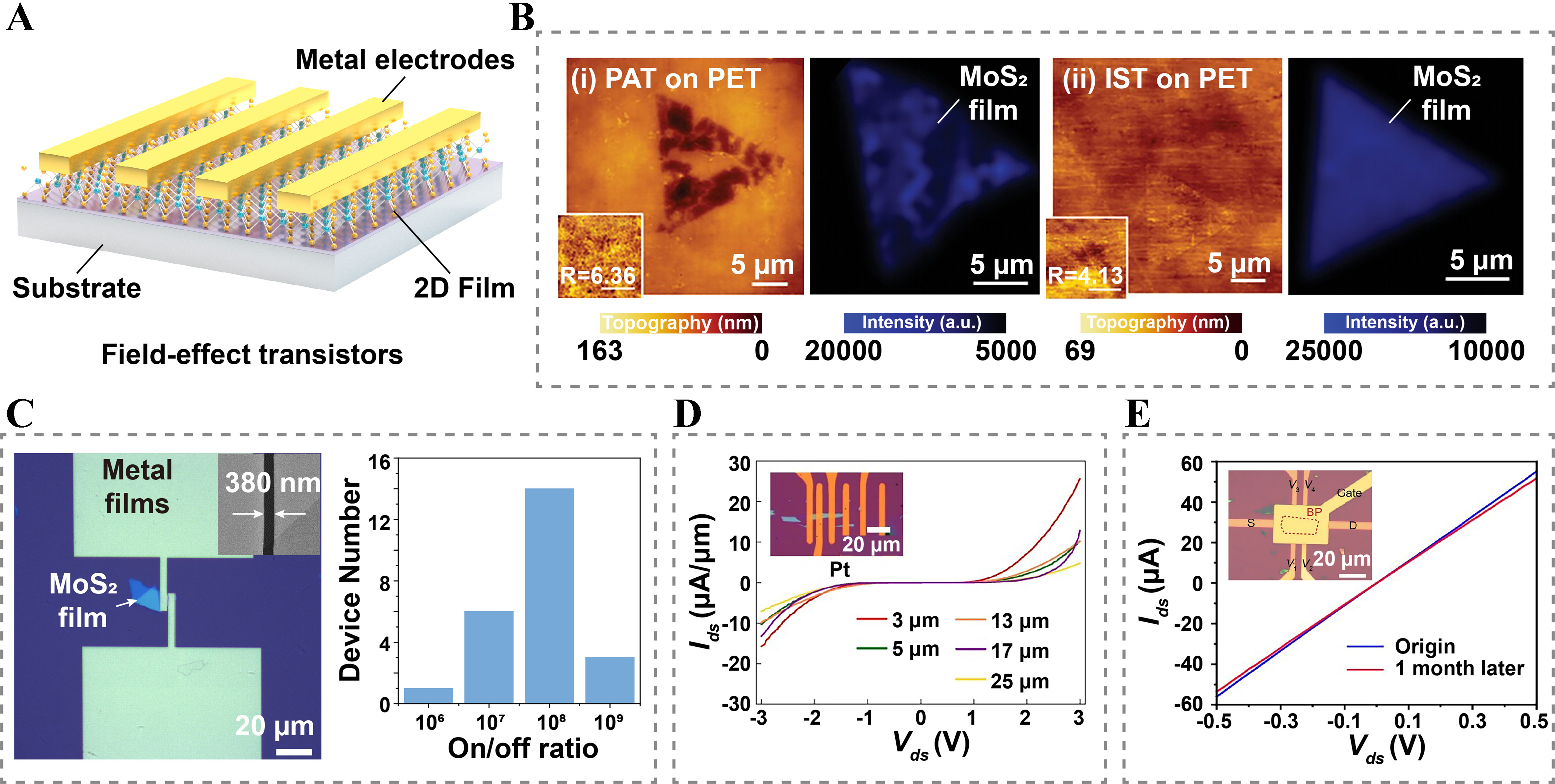
Figure 11. Applications of 2D films-based electronics. (A) Schematic illustration of the FETs; (B) AFM topographic images of MoS2 on PET by PAT and IST, respectively. Reproduced with permission[78]. Copyright 2023, Wiley-VCH; (C) Morphological characterization of the transistor with a channel of 380 nm and its statistical histogram of the ON/OFF ratio of 24 MoS2 transistors with different channel lengths on a SiO2/Si substrate. Reproduced with permission[71]. Copyright 2023, IOP Publishing; (D) Ids-Vds output curves of the MoS2 transistors using transferred Pt electrodes with different channel lengths at back-gate voltage of 60 V. Reproduced with permission[44]. Copyright 2022, Springer Nature; (E) The Ids-Vds curves of the device in the Inset, preserving linear ohmic contact even after exposure to air for one month. Inset: Typical OM image of the fabricated top-gated BP hall-bar device. The dashed line marked out the underlying BP sheet with a thickness of ~11.5 nm. Reproduced with permission[77]. Copyright 2025, Springer Nature. 2D: Two-dimensional; FETs: field-effect transistors; AFM: atomic force microscopy; PET: polyethylene terephthalate; PAT: PMMA-aided transfer; IST: ice stamp-based transfer printing; OM: optical microscope; BP: black phosphorus.