




Ultra-strong tungsten wire with high-proportion coincidence site lattice grain boundary
 0
0 Abstract
Tungsten wire, known for its high strength, has been developed for more than one century, but the understanding of its microstructure and deformation mechanisms remains limited, so do its applications. Near 6 GPa ultra-strong tungsten wires were prepared with help of cerium oxide addition. The fiber grains in the tungsten wire were refined from 399 to
Keywords
INTRODUCTION
Tungsten, known for its exceptional hardness and highest melting point among metals, has found extensive applications as high-temperature components for over a century. Today, as the tensile strength of mass-produced high-carbon steel wire already has approached its strength limit, tungsten, which possesses a much higher elastic modulus, heat-resistance and wear resistance, has become the ideal material for manufacturing ultra-strong diamond-cutting wires used in slicing silicon wafers for photovoltaic power generation in the green energy industry[1-4]. The tungsten wire is also an ideal candidate for reinforcing fibers in metal matrix composites for high-temperature applications[5-8].
Tungsten can withstand severe plastic deformation, such as rolling and drawing, which refines its macro size and microstructure and enhances its strength[9]. In addition, heavily deformed tungsten wires and sheets also show good tensile ductility, with a large local elongation at the necking zone. Therefore, it is of both scientific and industrial interest to heavily deform tungsten wires and sheets for strength enhancement, thereby expanding the application of tungsten as a key structural material[8,10,11]. Riesch et al.[8] reported that heavily drawn tungsten wires achieved a strength of 4.5 GPa. Fuhr[12] prepared 16 μm tungsten wire with a strength around 4.8 GPa, and further investigated the deformation mechanisms of drawn tungsten wire. Element-doping and oxide additions, such as potassium-doping and rare-earth oxide addition[10], have been demonstrated to strengthen tungsten and enhance its heat resistance[10,13-15]. However, the theoretical strength of tungsten is estimated to be 18 GPa, which is four times the highest reported value[16]. In comparison, pearlitic wires, which have been studied more extensively, can achieve half of their theoretical strength[17]. It follows that there is still significant potential for increasing the strength of tungsten.
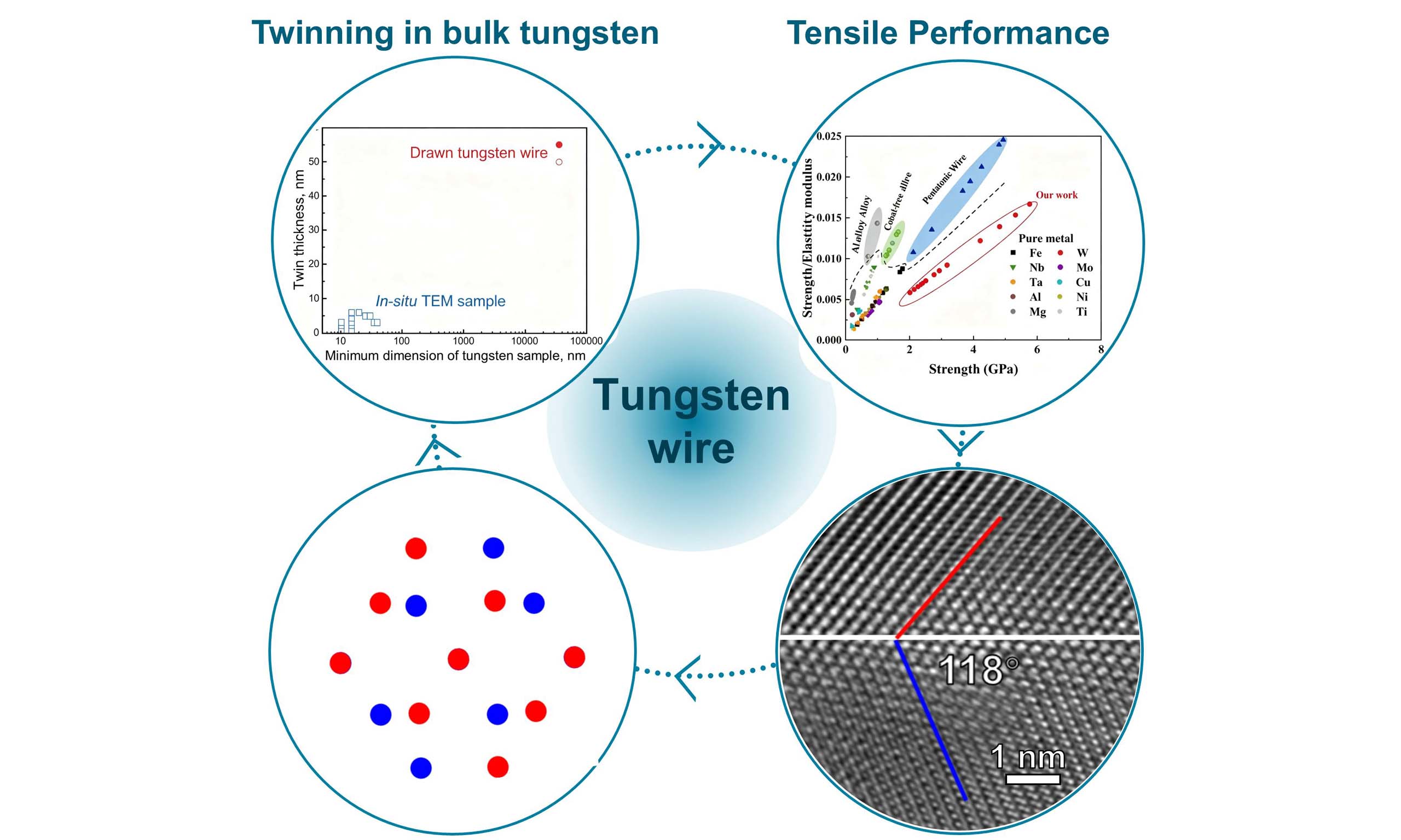
Research on the microstructure of heavily deformed tungsten is still at an early stage compared to other heavily deformed metals or alloys[18-22]. Regarding the plastic deformation of tungsten, existing research findings are similar to those for other body-centered cubic (BCC) metals in terms of dislocation glide, texture evolution and grain morphology evolution[23]. A high fraction of coincidence site lattice (CSL) boundaries, especially Σ3 boundaries, has been reported in drawn tungsten wires and deformed plates[24-27], and these Σ3 boundaries are proposed to originate from <110> fiber textures[24,27-29]. CSL boundaries are low-energy boundary structures which are typically produced by thermal processes[30]. Mechanical twinning is another mechanism responsible for generating CSL boundaries, i.e., Σ3 twin boundaries. Although the stacking fault energy, which determines the critical stress for twinning, is higher than 1,800 mJ/m2 for pure tungsten, {112} twinning can be activated in nano-scale tungsten samples, for example, in tensile samples for in-situ transmission electron microscopy observations[31-36]. To date no significant twinning has been observed in bulk tungsten samples.
In the present study, by adding cerium oxide and applying heavy drawing, the tungsten wire was strengthened to nearly 6 GPa. The microstructure in heavily drawn tungsten wires was investigated in detail. After drawing to high strains, oxide particles are distributed primarily at grain boundaries, suppressing dynamic grain coarsening caused by boundary migration and triple junction (TJ) motion. Surprisingly, a high proportion of twin structures was observed, suggesting that mechanical twinning may play a key role during the drawing process. This work provides an essential understanding of the deformation mechanisms in heavily drawn tungsten wires, demonstrating the large potential for further microstructural refinement and strengthening of tungsten wires far beyond 6 GPa.
MATERIALS & METHODS
The raw material used in this work was a commercially tungsten rods, which is a high-purity tungsten containing 0.5 wt.% (1.5 vol.%) cerium oxide particles produced and sold by Zhenjiang yuanshi advanced materials Co.,Ltd. The tungsten rods were prepared by powder metallurgy and sintered to a rod with a diameter of 18 mm. Then, the rod was first hot forged and rolled at a temperature higher than 1,800 K and subsequently hot drawn at 1,200 K to obtain a submicron-sized microstructure. The hot-drawn tungsten wires with a diameter of 390 μm were annealed at 1,400 K for 4 s before the final drawing process. The
Information of the tungsten wire samples analyzed in this study
| Diameter (μm) | Strain, ε | Area reduction | Strain rate, s-1 |
| 390 | 0 | 0 | / |
| 161 | 1.77 | 83% | 8.5 × 10² |
| 85.5 | 3.04 | 95% | 1.6 × 10³ |
| 52.9 | 4.00 | 98% | 3.9 × 10³ |
| 39.1 | 4.60 | 99% | 5.2 × 10³ |
| 34.1 | 4.87 | 99.2% | 7.9 × 10³ |
The tungsten wires were mounted in epoxy resin, followed by mechanical grinding and polishing. Finally, the samples were polished by an ion-milling system (Gatan 691 PIPS) before electron backscatter diffraction (EBSD) inspection. Samples for transmission Kikuchi diffraction (TKD) and high-resolution transmission electron microscopy (HR-TEM) experiments were prepared either by the above ion milling or the focused ion beam (FIB) milling.
Tensile testing of tungsten wires was carried out using a CMT4503 universal material testing machine at room temperature (~300 K) with a tensile strain rate 3.3 × 10⁻⁴ s-1. At least three samples for each drawing strain were measured to ensure the accuracy and reliability of the mechanical testing results. TKD (at an acceleration voltage of 30 kV) and FIB for sample preparation were carried out either in a ZEISS Crossbeam 350 SEM Crossbeam or a Crossbeam 550 SEM equipped with a Symmetry S2 detector. The scanning steps for EBSD and TKD were 6 to 100 nm based on the microstructure parameters of the tungsten wires. The EBSD data were analyzed using the software Aztec Crystal (Oxford), and a cut-off misorientation angle of 5° was applied for boundary detection. The CSL grain boundaries were determined by the Brandon criterion[37]. Due to the morphology of tungsten grains in heavily drawn wire, the grain boundaries were assumed to be perpendicular to the cross-section when determining the CSL boundaries based on the EBSD and TKD data. The TEM investigation used either an FEI-Tecnai G2 or a Talos F200X HR-TEM, both operated at 200 kV. The atom probe tomography (APT) specimens were prepared by Ga FIB milling using a FEI Helios G4 FIB-SEM with a standard lift-out procedure. The APT measurements were performed with a local electrode atom probe (LEAP 5000XR) under UV laser pulsing at a pulse energy of 100 pJ, a pulse repetition rate of 125 kHz and a target evaporation rate of 1% per pulse at 50 K. The reconstruction and quantitative analysis of APT data were performed using the visualization and analysis software CAMECA (AP Suite 6.3.2.125).
RESULTS
Evolution of microstructure
The microstructure (in both the longitudinal section and the cross section) and texture of the tungsten wire at ε = 0 are presented in Figure 1. The grains in the wire exhibit a typical fiber microstructure along the drawing direction and quasi-equiaxed morphology in the cross-section, as well as a strong <110> fiber texture [Figure 1A]. As shown in the Backscattered Electron (BSE) image of the cross-section, some of the cerium oxide particles were embedded inside the grains, while most of them were located at the grain boundaries or TJs [Figure 1B]. Statistical analysis of the particle size distribution of cerium oxide shows that the long axis of the oxide particles is approximately 0.085 μm, and the short axis is approximately 0.018 μm. EBSD results of the cross section and longitudinal section of the wire are presented in
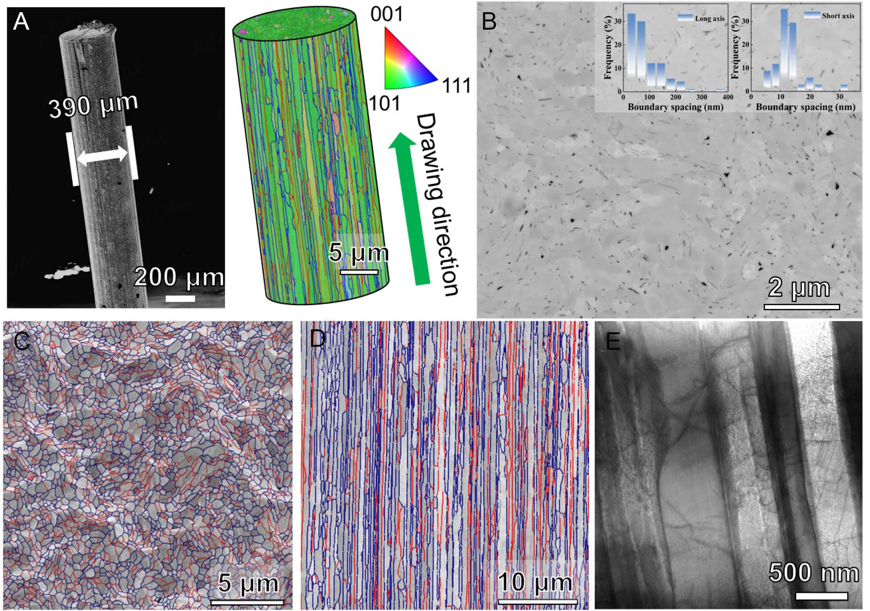
Figure 1. Microstructure of the tungsten wire at ε = 0 (390 μm). (A) SEM micrograph and corresponding illustration (IPF coloring based on the drawing direction) of the sample; (B) BSE image showing the distribution of cerium oxide; (C) Cross-sectional EBSD map, where low-angle grain boundaries (LAGBs, 5°-15°) and high-angle grain boundaries (HAGBs, > 15°) are marked as red and blue lines, respectively; (D) Longitudinal section EBSD map; (E) TEM micrograph showing the fine scale boundary and dislocation structure in a longitudinal section.
To reveal the origin of the ultra-high strength and microstructure evolution of the present tungsten wires, electron microscopy analysis of the wires was carried out. EBSD results revealed that the fiber grains were continuously refined during the drawing process; that is, the grains were elongated along the drawing direction and the cross-section of grains became finer as the drawing strain was increased [Figure 2]. As presented in Figure 2E and Supplementary Figure 1, all the drawn wires possess a strong <110> fiber texture. While the [110] direction of almost all the fiber grains are aligned along the drawing direction, the corresponding [101] direction (as marked by a dashed line in Figure 2E) shows a random rotation about the [110] axis [Figure 2F], hence showing a well-developed <110> fiber texture.
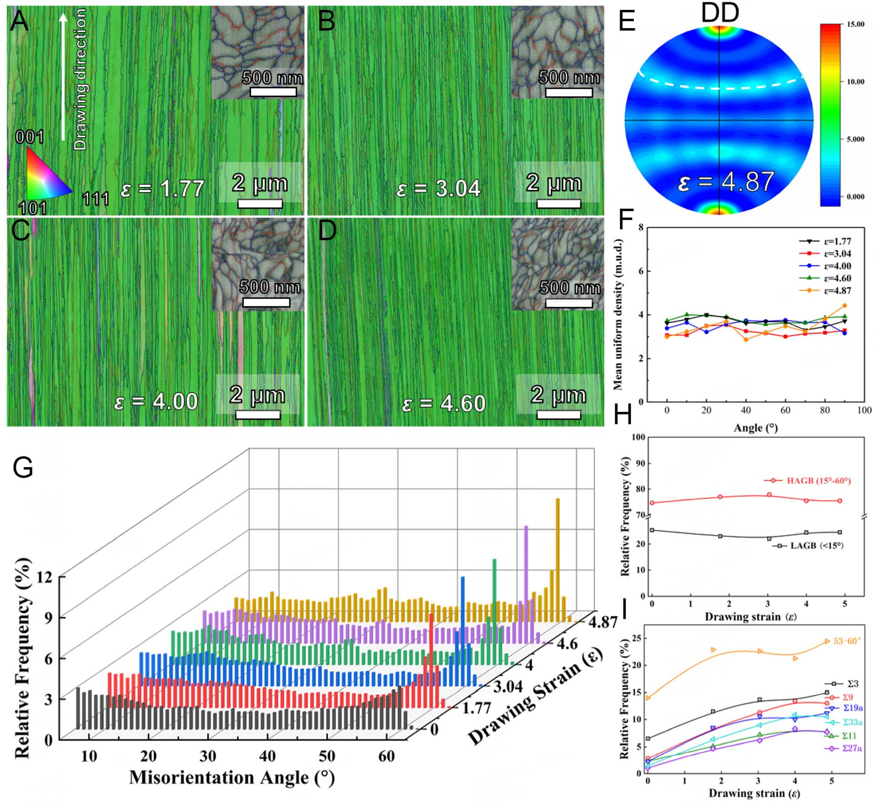
Figure 2. EBSD micrographs (IPF coloring based on the drawing direction) of the longitudinal and cross-sections of the drawn tungsten wire at different strains and texture analysis: (A) ε =1.77; (B) ε = 3.04; (C) ε = 4.00; (D) ε = 4.60; (E) Pole Figure of <110> of the tungsten wire at ε = 4.87 (DD is the drawing direction). (F) The intensity along the dashed line shown in (A) for different strains. The grain boundary characteristics of tungsten wires from EBSD and TKD results: (G) Grain boundary misorientation angle distribution; (H) Percentage of high and low angle grain boundaries; (I) Percentage of high angle grain boundaries with a misorientation of 53°-60° and coincidence site lattice grain boundary. Line in (H and I) are for guiding eye.
In terms of the grain boundary (GB) misorientation angle, there is a high proportion of high-angle grain boundaries (HAGBs) in all the tungsten wires. The proportions of HAGB and low angle grain boundary (LAGB) are stable, around 75% and 25%, respectively [Figure 2G and H]. There is a dominant range of GB misorientation angles, namely 53°-60°, which is consistently observed in all the drawn tungsten wires
To further analyze the GB characteristics, CSL boundaries are determined based on the EBSD and TKD results. Σ3, Σ9, Σ11, Σ19a, Σ27a, and Σ33a boundaries are confirmed to exist in the drawn tungsten wires [Figure 2I]. Notably, all these CSL boundaries are <110> symmetric tilt boundaries as presented in Table 2 although the Σ3 boundary may be also considered as 60°/<111>. The frequencies of all these CSL boundaries exhibit an increasing trend as the strain is increased. Moreover, the Σ3 GB prevails. For instance, the Σ3 boundary accounts for nearly 15% in the tungsten wire at ε = 4.87.
The rotation axis, rotation angle and accepted deviation angle for the CSL boundaries presented in the tungsten wires, as measured from EBSD and TKD result
| CSL boundaries | Rotation axis | Rotation angle (°) | Accepted deviation angle (°) |
| Σ3* | 111 | 60.0 | 8.66 |
| Σ9 | 110 | 38.9 | 5.00 |
| Σ11 | 110 | 50.5 | 4.52 |
| Σ19a | 110 | 26.5 | 3.44 |
| Σ27a | 110 | 31.6 | 2.89 |
| Σ33a | 110 | 20.1 | 2.61 |
Despite the tungsten wires possessing high proportional CSL GBs, the microstructure in the longitudinal section simply shows elongated fiber grains possessing a high density of dislocations [Figure 3]. The dislocation configuration is determined by the dislocation gliding mode and the interaction between dislocations and various obstacles during plastic deformation. The dislocations in the tungsten wire at
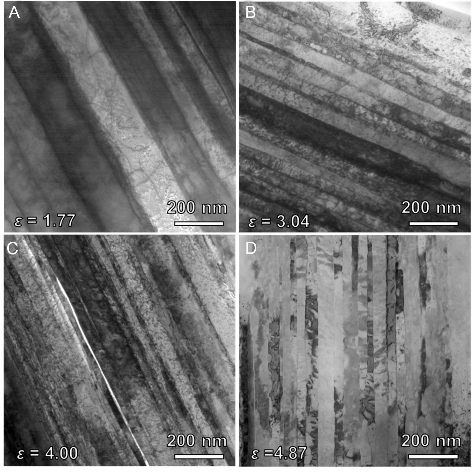
Figure 3. TEM imaging of grain boundaries and dislocation structures in the tungsten wires: (A-D) TEM images of tungsten wire corresponding to strains of 1.77, 3.04, 4.00, and 4.87.
The distribution of cerium oxide in the tungsten wire at ε = 4.87 was inspected by STEM-EDX and APT [Figure 4]. A schematic diagram of the proportion of oxides to grain boundaries is drawn in Figure 4B, from which it can be seen that some oxides are embedded at the TJ and grain boundaries on the cross section of the wire. The cerium oxides occupy 13% of the total length of the grain boundaries. Further analysis by APT was carried out for the wire at ε = 4.87. The 3D atom map shows cerium-rich regions parallel to the drawing direction [Figure 4C]. Quantitative analysis across one cerium-rich region was performed. In the concentration profile, the average cerium concentration is equal to that of the oxygen, suggesting that the cerium exists in the form of CeO, while the CeO segregation thickness is 4 nm here which should correspond to the fine CeO layer obseved in EDX mapping. A concentration profile in a cerium-free region shows practically 100% tungsten, suggesting that neither Ce nor O are not dissolved in tungsten due to the high thermal stability of CeO.
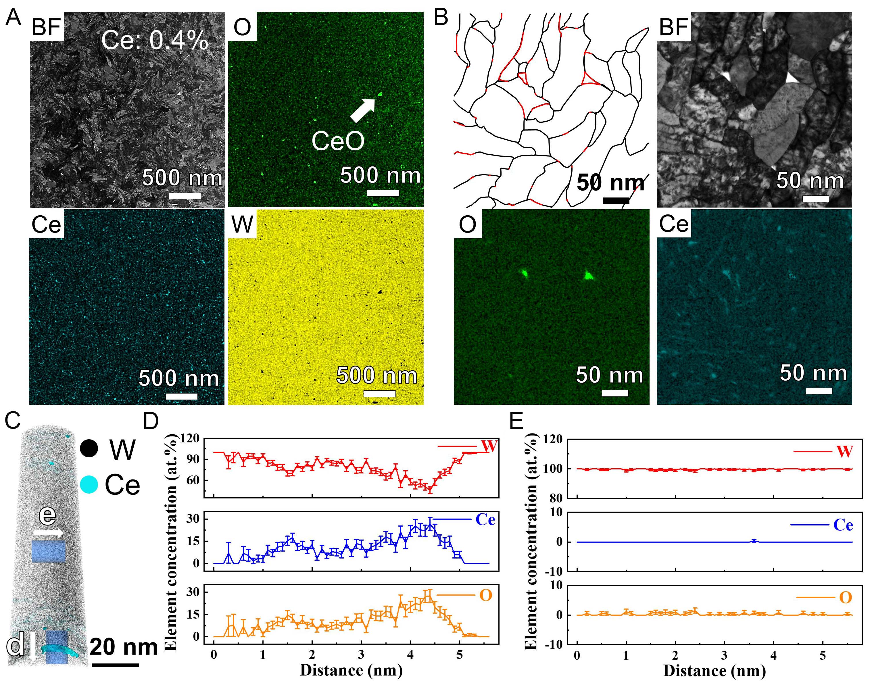
Figure 4. Chemical analyses of tungsten wire: (A and B) Element distribution maps of tungsten wire at ε =4.87 obtained by STEM-EDX on the cross-section of the tungsten wire with a schematic diagram in (B) showing the distribution of CeO on the GBs; (C) 3-D cerium atom maps of tungsten wire with a drawing strain of ε = 4.87, showing a 10 at.% cerium iso-concentration surface (cyan), together with selected regions of interest (ROI); (D and E) concentration profiles for the ROIs in (C) along or perpendicular to the needle direction. The drawing direction is horizontal. The error bars represent the standard deviation (Sigma) of atomic concentration output by CAMECA software.
Microstructural feature statistics of the tungsten wires determined based on both the EBSD and TEM observations (see e.g., Figures 2 and 3) are presented in Table 3. When the strain is increased from 0 to 4.87, the average boundary spacing decreases from 399(±55) to 39(±6) nm. Meanwhile, the ratio between the diameter of the wire and the average boundary spacing decreases by only 12% when drawn to a strain of 4.87.
Relationship between tungsten wire diameter and fiber boundary spacing
| Drawing strain | Diameter (μm) | Boundary spacing (nm) | Diameter/Boundary spacing | Yield strength σ0.2, MPa |
| 0 | 390.0 | 399 ± 55 | 978 ± 156 | 2,100 ± 60 |
| 1.77 | 161.0 | 179 ± 18 | 899 ± 106 | 2,811 ± 79 |
| 3.04 | 85.5 | 89 ± 10 | 965 ± 104 | 3,702 ± 108 |
| 4.00 | 52.9 | 59 ± 6 | 895 ± 97 | 4,321 ± 135 |
| 4.60 | 39.1 | 48 ± 8 | 809 ± 158 | 4,940 ± 148 |
| 4.87 | 34.1 | 39 ± 6 | 863 ± 167 | 5,440 ± 161 |
CSL boundaries
In the present work, the Σ3 boundary is the most prevalent among all CSL boundaries. We therefore focused on revealing the detailed features of the Σ3 boundaries in order to understand their origin. All the detected CSL boundaries are <110> symmetric tilt boundaries, and the <110> zone axis is also the preferred observing direction for {112}<111> twin in tungsten[34]. Hence, the cross-section of tungsten wire drawn to the maximum drawing strain ε = 4.87, having the highest fraction of CSL boundaries and a strong <110> fiber texture, was selected for further investigation.
Figure 5 shows the cross-section of the tungsten wire at ε = 4.87. A total of 271 Σ3 boundaries were identified and classified into two characteristic types. For the first type, one grain forms two Σ3 boundaries with its neighbors on two opposite sides as presented in Figure 5C1-C4, also marked with dashed circles in
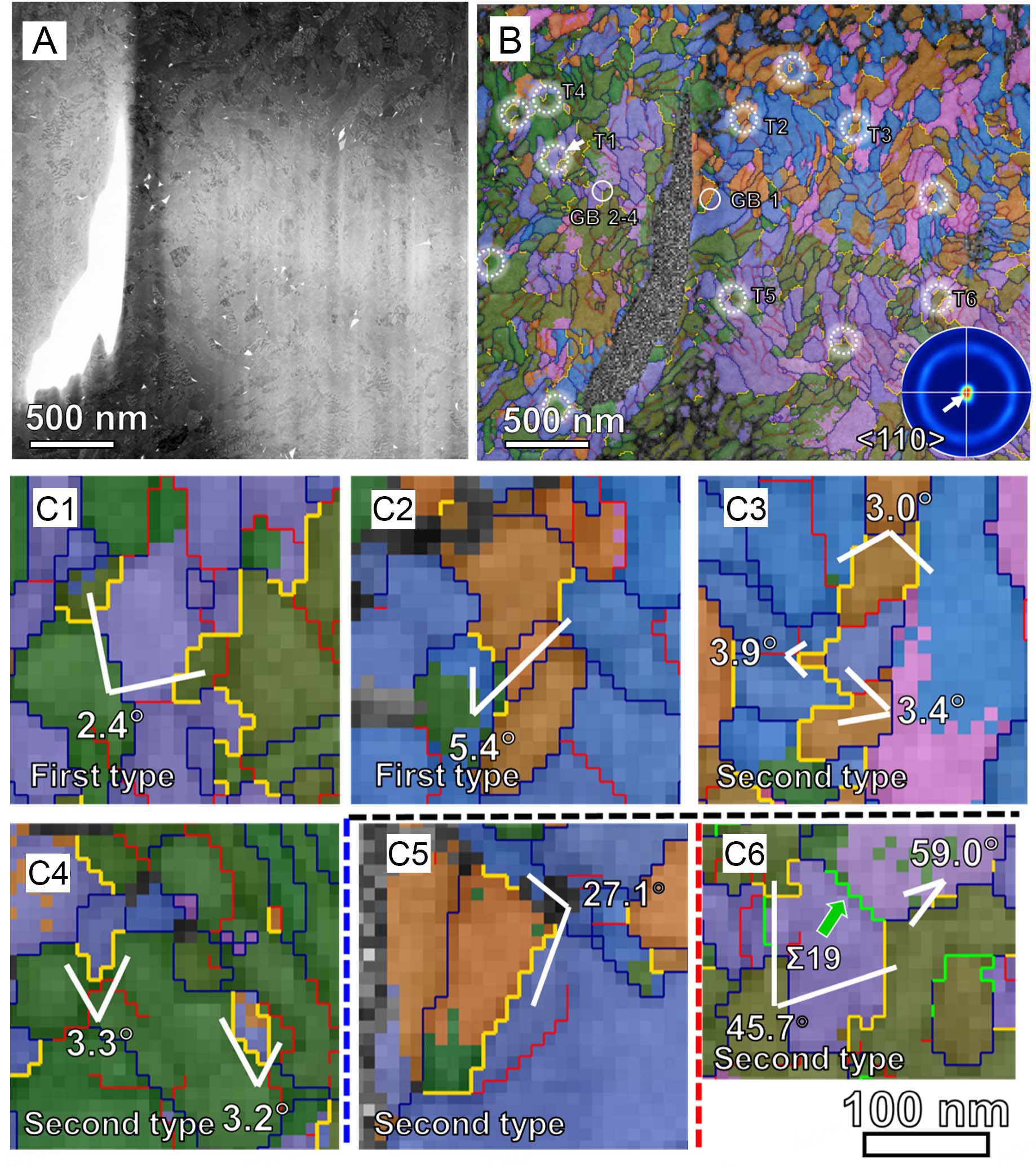
Figure 5. TEM micrographs and corresponding TKD maps of tungsten wire at ε = 4.87 taken from the cross section (i.e., looking along the drawing direction): (A) TEM micrograph; (B) Corresponding TKD map (Euler coloring map); (C1-C6) Typical features of Σ3 boundaries in the wire. The navy line, red line, orange line and green line are HAGBs, LAGBs, Σ3 boundaries and Σ19 boundaries, respectively.
The feature of the first type is shown in Figure 6. The two separated paired grains have a small misorientation angle of 2.4° (Figure 6A is vertically flipped, 45° rotated from Figure 5C1 and shown in IPF colour). The crystallographic orientations of the three grains (C1, C2 and C3) are illustrated using {110}, {112} and <111> pole figures, as shown in Figure 6B. A crystallographic orientation relationship equivalent to {112}<111> twin can be identified between the grain C2 and the separated paired grains (C1 and C3). They share one of the <111> directions, as well as the three {112} planes parallel to that <111> direction, and one of the shared {112} planes is also parallel to the two Σ3 boundaries. The Σ3 boundaries exhibit weak contrast in the bright field TEM micrograph [Figure 6C]. NBD patterns further confirm the twin orientation relationship [Figure 6C1-C3]. The atomic scale structures of the two Σ3 boundaries are also presented in Figure 6C. The HRTEM micrographs and corresponding FFT analyses in Figure 6D1-D4 demonstrate that the two boundaries are strict Σ3 twin boundaries (Σ3 TBs). In other words, Figure 6 presents a structural feature consistent with both the morphology and crystallography of a {112}<111> BCC-twin.
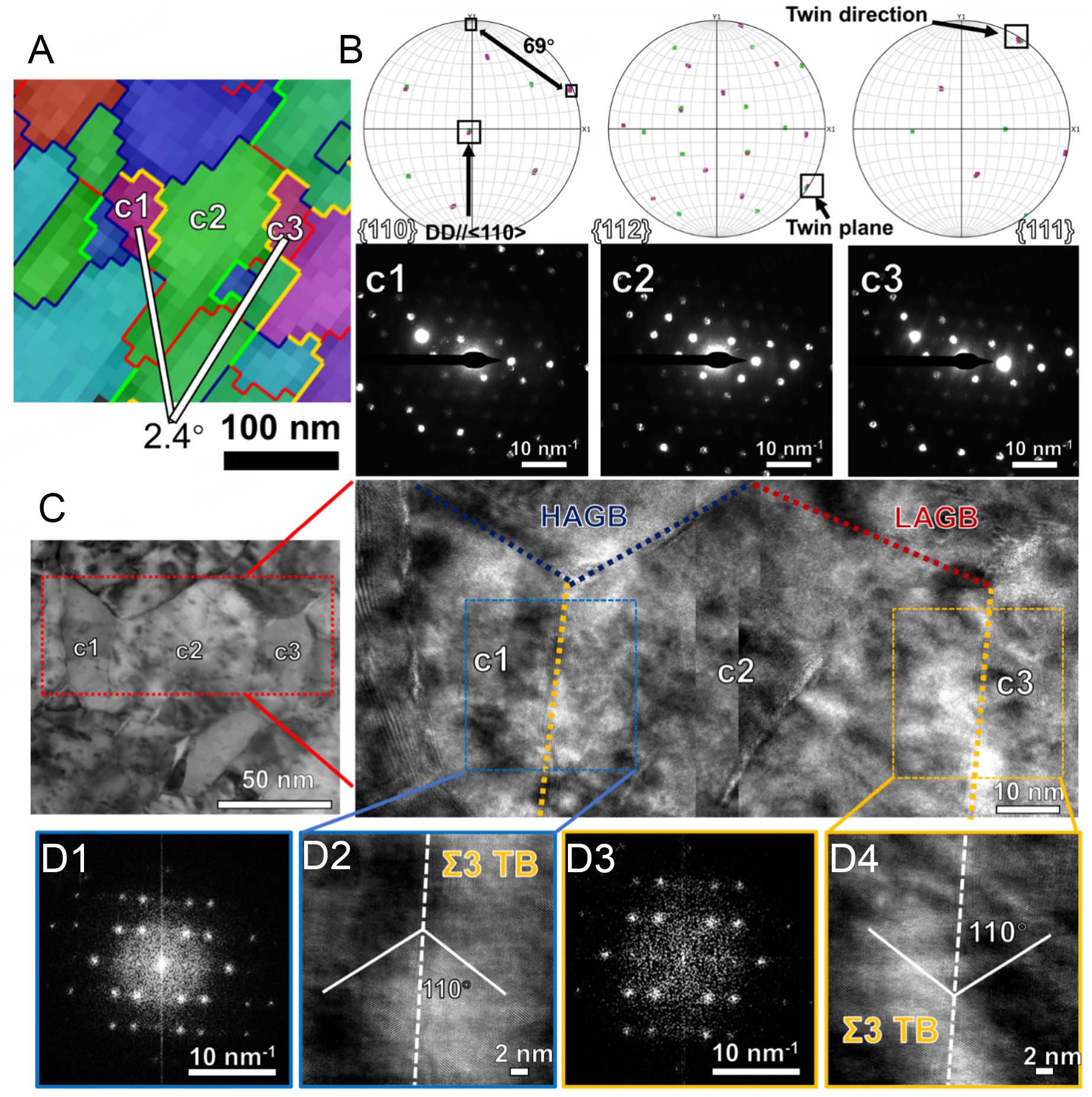
Figure 6. TKD maps and TEM micrographs of tungsten wire at ε = 4.87 taken from the cross section (A) TKD IPF coloring map. Orange line: Σ3 boundary, Blue line: HAGB, Red line: LAGB; (B) IPF pole figures. (C) Corresponding bright field STEM micrograph and corresponding HRTEM micrograph, (C1-C3) the NBD patterns of the (C1) to (C3) in (C), the zone axis is near to [110]W. (D1-D4) atomic scale structure and corresponding FFT analyisis of the two Σ3 twin boundaries.
The feature of the second type [Figure 5C6] is exhibited in Figure 7. The misorientation angles of the three GBs, as marked in Figure 7A, are 59.5° (GB-2), 27° (GB-3) and 58.5° (GB-4), respectively. The three boundaries are identified by TKD as Σ3 (GB-2), Σ19 (GB-3) and a normal HAGB (GB-4). The atomic scale structures of the TJ and GBs are revealed by HRTEM [Figure 7B and C1-C3]. GB-2 appears to be a standard Σ3 GB, where the angle between the two (110) planes is 110°. The angle between the two (110) planes on either side of GB-3 is 153°, which is close to the ideal condition for a <110>-tilt Σ19 GB. Notably, GB-3 does not connect to the TJ directly. There is a 5-nm-long boundary connecting GB-3 to the TJ [Figure 7B]. Although separating the same two grains as GB-3, the 5-nm-long boundary is not a coherent Σ19 GB due to the lack of symmetry of the GB plane [Figure 7C3]. The non-CSL boundary GB-4 also exhibits an interesting feature, namely that the two (110) planes with an angle of 97° are symmetrical along GB-4. Another area is presented in Supplementary Figure 2, which contains a TJ with a similar feature to that in Figure 7. Two differences are: (i) the Σ3 GB (GB-6 in Supplementary Figure 2C2) is imperfect as the boundary plane is not symmetrical with the two (110) planes; and (ii) the normal HAGB GB-5 (in Supplementary Figure 2C1) shows a precise 90° tilt about the <110> axis. A stereographic projection along the [110] direction of tungsten [Supplementary Figure 3] shows that rotating one grain about the common [110] axis gradually transforms GB-5 (90° rotation) to GB-4 (97°), GB-2 (110°) and GB-6 (118°).
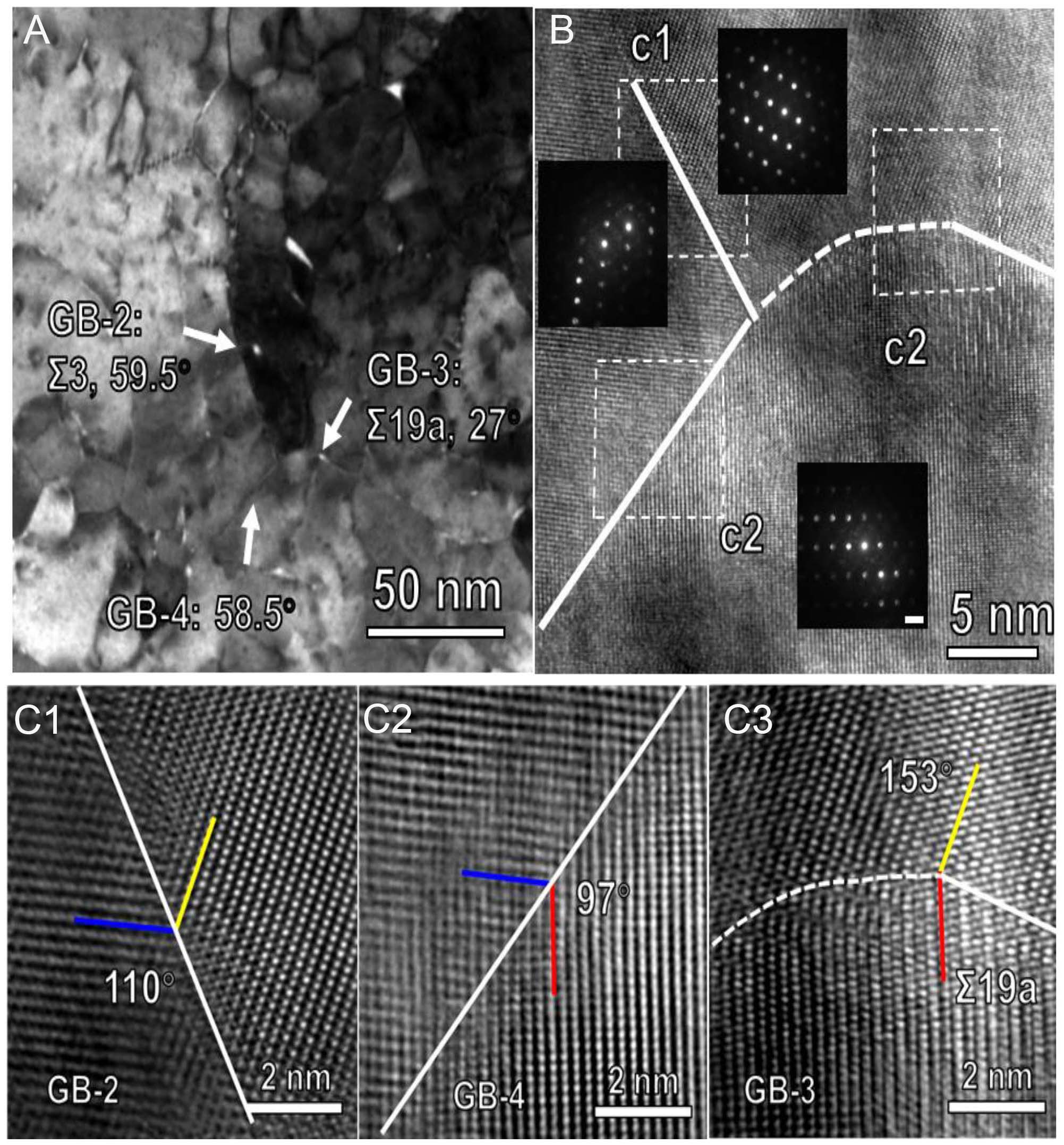
Figure 7. TEM micrographs of the triple junctions marked by white circles in Figure 5C6: (A and B) TEM and HRTEM micrographs of the triple junctions, the NBD patterns show the three grains were observed near to [110]W; (C1-C3) HRTEMs for GB-2, GB-3 and GB-4, respectively. The scale bar for nano beam diffraction patterns is 5 nm-1.
Fiber textures revisited
Since the Σ3 boundary is associated with a rarely reported twin structure in tungsten, the following analysis in the longitudinal section of the tungsten wire at ε = 4.87 focuses on the grains containing the Σ3 boundary. The EBSD result here is presented using an Euler-colouring map to clearly show the different grains. First, separated paired grains, forming Σ3 boundaries with the fiber grain between them, are marked in the red box in Figure 8A. The middle fiber grain has a length of 700 nm. The two separated grains exhibit a misorientation angle of 8.2°. The crystallographic orientations of the three grains are shown using pole figures in Figure 8B, corresponding to the {112}<111> BCC-twin relationship.
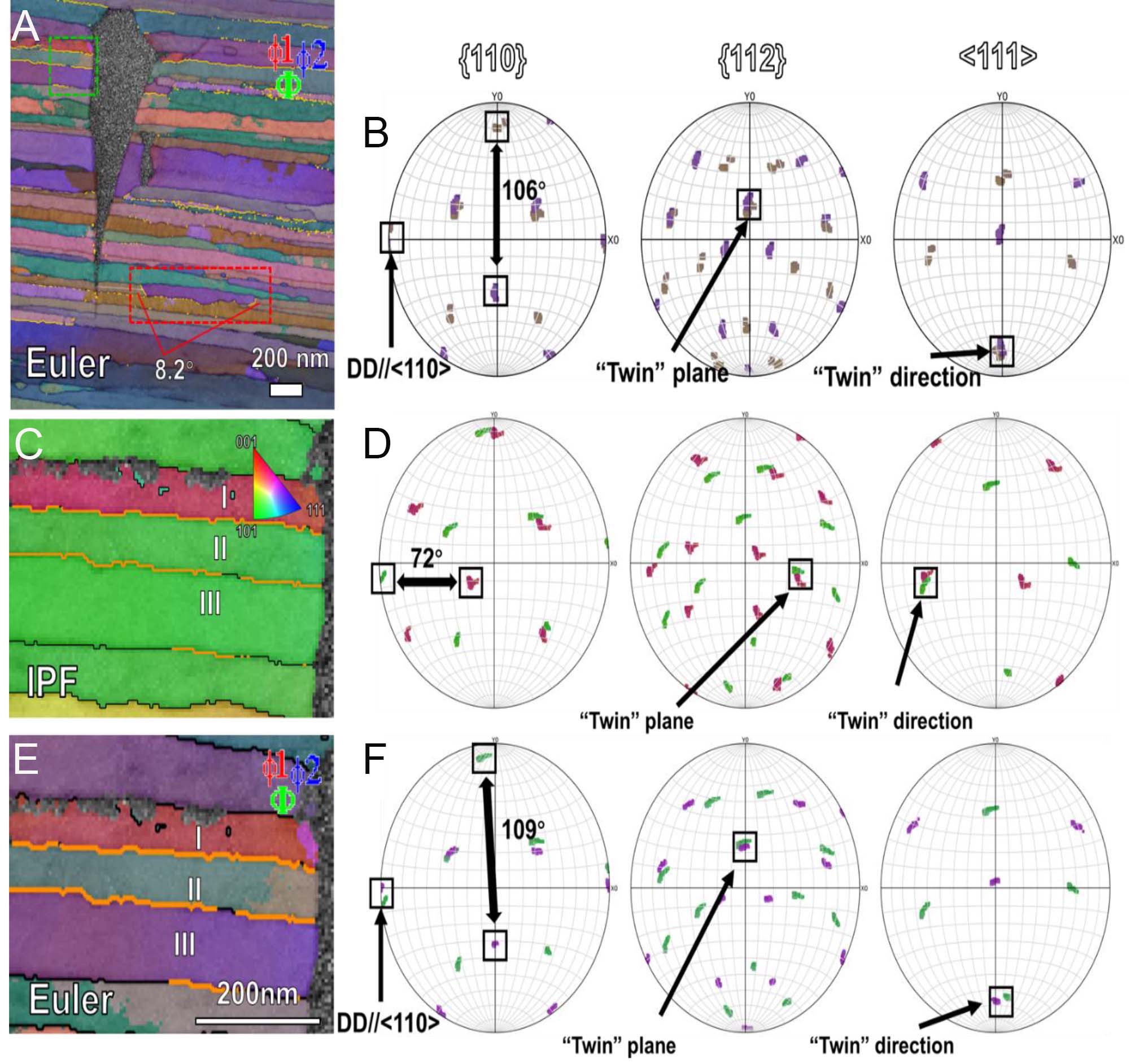
Figure 8. TKD maps and orientation analysis of tungsten wire at ε = 4.87 along longitudinal section: (A) TKD Euler-coloring map. The insert is the crystallographic analysis for the grains in red box; (B) Crystallographic orientaionship analysis for the red box in (A) using pole Figure. (C) IPF-coloring maps for the green box in (A and D) crystallographic orientaionship analysis of Fiber I and Fiber II. (E) Euler-coloring maps for the green box in (A) and (F) crystallographic orientaionship analysis of Fiber II and Fiber III.
Three fiber grains sharing Σ3 GBs along the drawing direction are marked in the green box in Figure 8A. As presented in Figure 8C and D, crystallographic orientation analysis shows that grain I does not exhibit <110> fiber texture although it shares a twin-like crystallographic relationship with grain II. This occurs because their nominal “twin” direction <111> was not perpendicular to the drawing direction. The <110> fiber texture is the stable texture for cold drawn BCC metals in which deformation is dominated by dislocation slip. The non-<110> textured fiber grain could not be explained by the result of dislocation gliding, while suggested that it may be a result of a twinning mechanism. In comparison, as shown in Figure 8E and F, the grain II and grain III, both exhibiting <110> fiber texture, share the nominal twin direction <111> perpendicular to the drawing direction.
Drawing strengthening
The tensile properties of the tungsten wires at different drawing strains are presented in Figure 9A and B. The tungsten wire at ε = 0 has an ultimate tensile strength (UTS) of 2.52 GPa and a uniform elongation of ~3%. Both the UTS and the 0.2%-offset yield strength (σ0.2) increase with the drawing strain monotonically. As the drawing strain ε is increased to 4.87, the UTS of the tungsten wire increases to 5.86 GPa, which is 133% higher than that of the sample at ε = 0. In contrast to coarse-grained bulk tungsten[22,42], the tungsten wire at ε = 4.87 deforms as a ductile metallic material during tensile testing. It exhibits strain hardening [Figure 9A] and a ductile fracture with an area reduction of 37% at the necking area (insert in Figure 9B). The fracture surface is rough without obvious cleavage planes, showing a large number of dimple-like structures induced by dislocation slip and shear deformation traces between grains [Figure 9B]. Figure 9B reveal uniformly sized dimples and tear ridges distributed in the fracture region, with smooth inner walls of the dimples, reflecting significant plastic flow of grains during the deformation process.
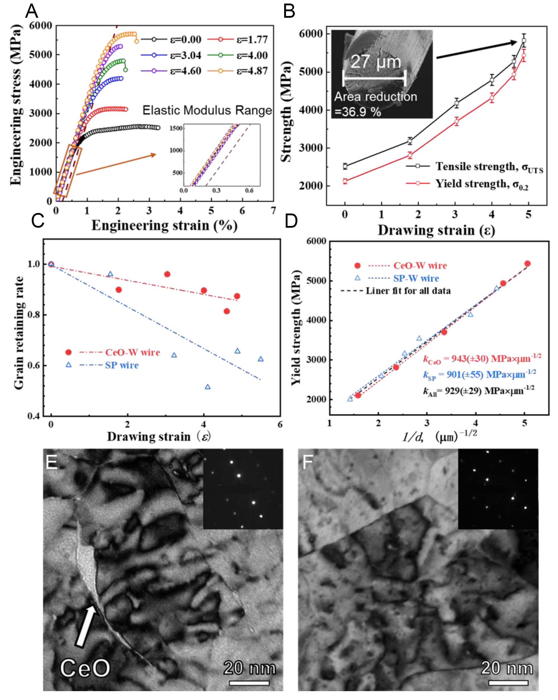
Figure 9. Mechanical properties of tungsten wire and the relationship between the strengthening of tungsten wire. CeO-wire: CeO-added tungsten wire, SP-wire: single phase tungsten wire without CeO addition: (A) Engineering stress-strain curves of tungsten wire with different strains (0, 1.77, 3.04, 4.00, 4.6, and 4.87); (B) Corresponding tensile strength and yield strength and fracture of tungsten wire at ε = 4.87 after tension, error bars denote standard deviation from measurements of no less than 3 specimens per group; (C) the grain retaining rate versus the drawing strain. (D) The relationship between the yield strength of tungsten wire and the boundary spacing D-1/2. TEM micrographs and corresponding NBD diffraction patterns of (E) CeO-added tungsten wire and (F) single phase tungsten wire at
DISCUSSION
The influence of cerium oxide
The present CeO-added tungsten wire possesses a tensile strength of 5.86 GPa. The high strength should first be attributed to the nano fiber grain, which is a result of the adopted processes, including sintering, forging, rolling, hot drawing and final drawing. Preparing processes before the final drawing results in a 390 μm tungsten wire possessing ultra-fine fiber grains with an average spacing of 399 nm. The final drawing process further refines the fiber grain to an average spacing of 39 nm. The final drawing temperature was set to 723 ± 50 K, which is equivalent to 0.2 melting point of tungsten (3,700 K) and is also equivalent to room temperature drawing for steel wire. Hence, thermal-induced recrystallization and recovery were suppressed during the final drawing process. More importantly, the oxide addition plays a key role in the drawing-induced grain refinement.
It is generally believed that oxides dispersed in the matrix strengthens it by acting as obstacles to dislocation motion, a mechanism known as oxide dispersion strengthening. In the present study, most of the cerium oxide is embedded at the grain boundaries or TJs, where it plays a dominant role in suppressing boundary motion. To illustrate the influence of this suppressing effect, high purity tungsten wires are prepared by the same process for comparison. The initial average boundary spacing of the CeO-free tungsten wire is 497 nm. It decreases to 66 nm at ε = 4.76. Detailed information can be found in
Based on the boundary spacing statistics, the strength evolution of the tungsten wires can be explained by the empirical Hall-Petch relation, which has previously been employed to determine the quantitative relationship between yield strength and grain size in various heavily drawn metals successfully. The formula of the Hall-Petch relation is[43-45]:
Among them, σ represents the yield strength of the material (σ0.2 in this study), σi is the intrinsic lattice friction stress, KY is the Hall-Petch slope, and D is the boundary spacing in this study instead of traditional equiaxed grain size. Because heavily drawn tungsten exhibits a fibrous microstructure elongated along the drawing direction, where boundary spacing rather than grain length is the key parameter controlling dislocation gliding stress. As presented in Figure 9D, the yield strength σ0.2 shows an approximately linear relationship with D-1/2, indicating that the strength of the heavily drawn tungsten wires follows the Hall-Petch relation, where σ0 and k are calculated to be 556 ± 111 MPa and 943 ± 30 Mpa·µm-0.5.
The value of the k is close to that of Cordero’s summary for a grain size range 0.16 m to 7 μm[46], where k is 1,000 MPa·μm-0.5. Notably, the CeO-free tungsten wire also follows the Hall-Petch relation, where k is calculated to be 901(±55) MPa·μm-0.5. The addition of cerium oxide shows a minor effect on the Hall-Petch slope. The reasons may be related to the distribution of cerium oxide. The majority of cerium oxide was embedded in the GB and cerium solubility in tungsten is negligible [Figure 4]. Therefore, there is little extra pinning effect on the threading dislocations in the lamellae/grains compared to pure tungsten wires after heavy drawing. Representative TEM micrographs exhibit the threading dislocation configurations in lamellae/grains for the CeO-added tungsten wires [Figure 3]. The lack of extra pinning effect also results in a similar dislocation density in the two tungsten wires. Figure 9E and F shows two tungsten grains, each having one dimension close to 50 nm, in both the CeO-added and CeO-free samples at ε = 4.87/4.76. The dislocation density in both samples is on the order of 1015 m-2. Unlike other metallic materials, which undergo significant deformation-induced dissolution of the second phase and release the dislocation-pinning solutes (such as carbon in pearlitic steel wire[17,47,48]), the dynamic recovery of dislocations in tungsten lamellae/grains during cold drawing seems to be hardly influenced by solute elements from cerium oxide due to their very low concentration. Therefore, it can be further proposed that the addition of cerium oxide has a minor effect in directly influencing the dislocation behaviors in lamellae/grains for the heavily drawn tungsten wires, but it significantly enhances the drawing-induced strengthening of the tungsten wire by suppressing dynamic grain coarsening during the drawing process.
Grain boundary characteristics
The present heavily drawn tungsten wires have a high fraction of HAGBs, as well as a peak at around 60°. Half of the peak is due to the Σ3 GBs. This peak may be related to mechanical twinning, which produces Σ3 GBs. However, this peak may also be related to the strong <110> fiber texture as can be revealed by a simple calculation[28]. If a perfect <110> fiber texture with random distribution of grains is assumed, which is close to the present case, the resulting misorientation angle distribution is shown in Figure 10A. For misorientation angles smaller than 60°, the misorientation axis is <110>, corresponding to rotation about the fiber axis for 0°-60°. The rest 1/3 is close to 60°/<111>, corresponding to rotation about the fiber axis for 60°-90°. It should be noted that the texture could not be perfect in practice. The deviation from the perfect <110> fiber texture gives rise to the difference in the misorientation angle distribution shown in Figure 2G.
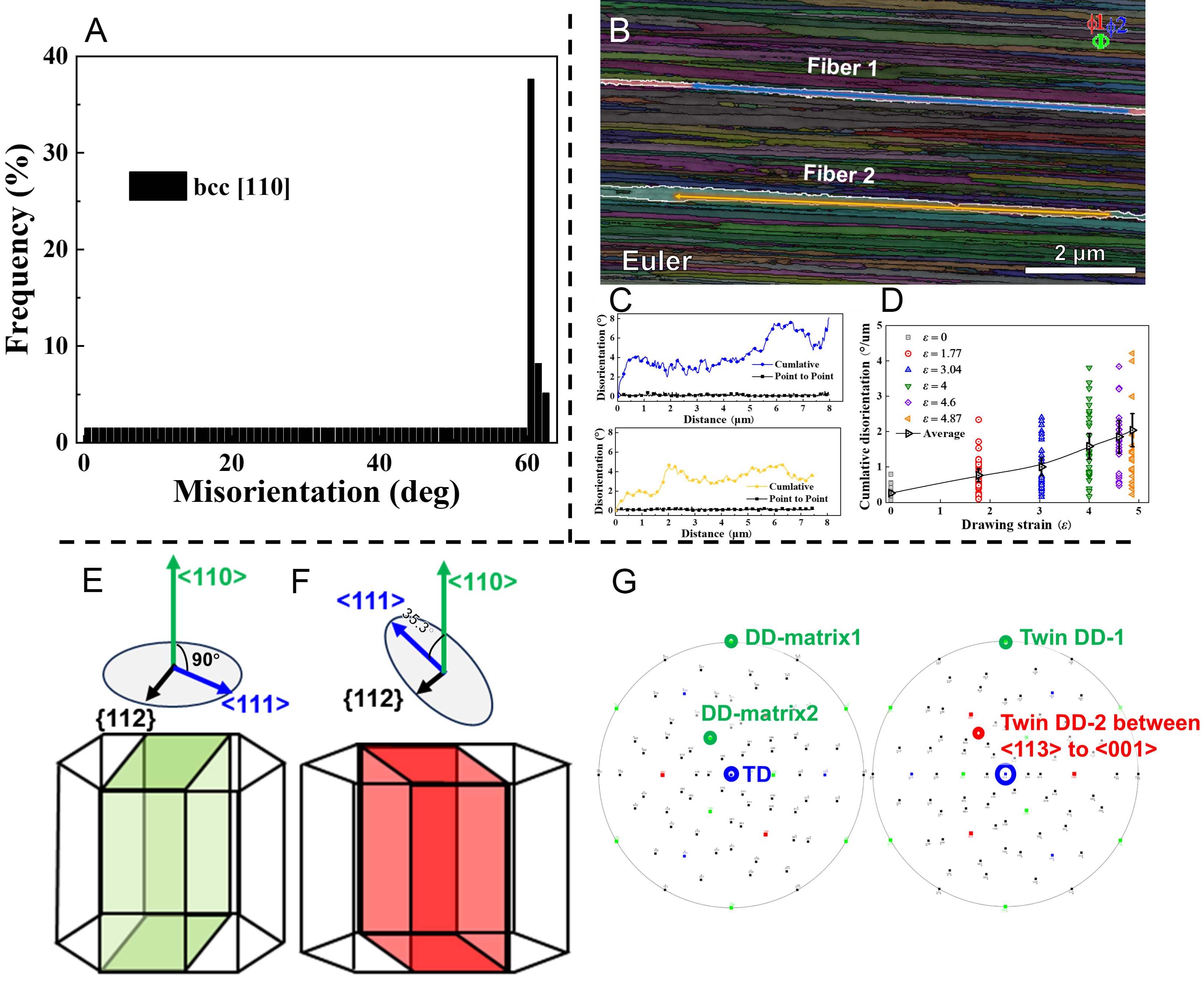
Figure 10. (A) The misorientation angle distribution of BCC metal with perfect <110> texture. Orientation changes along the drawing direction: (B and C) Two examples of measuring the cumulative misorientation in the tungsten fiber grains in the EBSD mapping result of tungsten wire at ε = 3.04; (D) Orientation gradient along the drawing direction in the tungsten fiber grains at different strains, error bars show standard deviation of cumulative misorientation. Schematic diagrams for showing the two types <111> twinning directions in present tungsten wires: (E) <111> twinning direction perpendicular to the <110> fiber texture/drawing direction; (F) <111> twinning direction 35.3° away from the <110>fiber texture/drawing direction; (G) Projection along a fixed <111> twinning direction. DD and TD are represented for the drawing direction and twinning direction, respectively.
The coupling of grain rotation and boundary relaxation may partly explain the formation of high fractional CSL GBs in the present tungsten wires. The strong <110> fiber texture provides the misorientation angle and axis needed for the <110>-tilted CSL boundaries. In addition, orientation gradient analysis shows that the average cumulative misorientation along the drawing direction increases monotonically with the drawing strain suggesting continuous grain rotation occurs during the drawing process [Figure 10B-D]. The microstructure evolution follows a principle of energy minimization during plastic deformation[49-51]. According to this principle, the evolving structure shields internal stresses to reduce the system energy. When neighboring grains exhibit the crystallographic orientation relationship of a <110>-tilted CSL GB, following the principle of energy minimization, the GB plane transforms toward the CSL GB configuration to reduce the boundary energy. GB-1 to GB-6 presented in Figure 7 and
These CSL boundaries are more stable than random HAGBs during the drawing process in three aspects. First, thanks to their low energies, CSL boundaries reduce the deformation stored energy, thereby reducing the driving force for grain coarsening during deformation and annealing[55]. Secondly, they have low mobility, possibly orders of magnitude lower than that of a random HAGB[37,55-60]. This is especially true for the TJs containing low-CSL coherent boundaries, which presents a significant energy barrier to ledge growth and kink nucleation due to their compact atomic arrangement. Third, the straight boundary plane of CSL boundaries suppresses the curvature-driven boundary migration[61-64]. Hence, as the strain is increased, more CSL boundaries are stored than random HAGB during the drawing process and increasing proportional CSL boundaries are identified.
Possible twinning in tungsten wire drawing
Evidence suggests that the some of the Σ3 boundaries observed in this tungsten wire may be associated with deformation-induced twinning, a phenomenon rarely reported in bulk tungsten. First, deformation twins in BCC metals such as W and Ta which possess high stacking fault energy, can exhibit a morphology quite different from those found in FCC metals. Specifically, they may present as irregular in shape, and their twin boundaries can be noticeably non-planar, often featuring numerous edges lying on the {112} planes[65]. In addition, the spacing between the two twin bundles can be larger, meaning the twins are relatively sparse[65-67]. The above characteristics make it difficult to identify twins in present tungsten wires through direct morphological observation alone; instead, it is relies on crystallographic relationships to determine where twinning might have occurred.
The increase in the amount of Σ3 GBs [Figure 2I] and the confirmation of twin-like microstructures at
Deformation twinning is generally hard to be activated in tungsten[66] or other BCC metals and alloys (reviewed in[68]). For coarse-grained materials, the occurrence of deformation twinning typically requires very low temperature and/or exceedingly large strain rates (through processes such as impact/shock[69-72] and dynamic shear[65]). For instance, Argon et al.[66] reported deformation twins in single crystal tungsten at 77 K, but no such twins at room temperature. Via molecular dynamics (MD) simulation on single crystal Tantalum in broad ranges of temperature (5-1,000 K) and strain rate (1 × 10⁶-7 × 10⁹ s-1), Zepeda-Ruiz et al.[73] proposed a threshold critical resolved shear stress of around 1.9 GPa for twinning in Tantalum, which is a bit higher than 1% of the elastic modulus. Deformation twinning was also observed in tungsten following high-velocity projectile impact, where the strain rate was estimated to exceed 103~106[33]. In contrast to the bulk materials, the requirements for twinning and even anti-twinning (the latter is believed much difficult to stimulate than the former) in nanowires[34,36,74] become largely alleviated. This can be rationalized by the fact of lack of plastic deformation carriers inside nanocrystals, which results in ultra-high stress and thus the unusual deformation mechanism.
By comparing the microstructure and the deformation parameters in this study with the ones in literature discussed above, the activation of deformation twinning during the tungsten wire drawing turns to be not surprising. Firstly, the drawing temperature for tungsten (723 ± 50 K, 20% of the melting point 3,700 K) was relatively low and the strain rate, increasing from 8.5 × 10² to 7.9 × 10³ s-1, was relatively high, both facilitating twinning. Secondly, the flow stress, estimated with the yield strength values of the wires after undergoing the multiple drawing passes, increased from about 2.5 to 5.4 GPa, which is expected to be sufficiently large for triggering the twinning mechanism.
We now focus on the crystallographic orientation of the twins. An example in a schematic in Figure 10E. Given the dominant <110> fiber texture of the tungsten wires, half of {112}<111> twinning variants would possess an <110> orientation along the wire axis after twinning [Figure 10F]. These variants’ <111> twinning direction is perpendicular to <110> fiber texture orientation (drawing direction and axial direction). Their 1/6[111] twinning dislocations on adjacent {112} planes[75] are hardly activated by the tensile stress along the axial direction (drawing direction); meanwhile, they also only contribute the strain along the radial direction, but have no contribution to the strain along the axial direction. The remaining half variants, which <111> twinning direction 35.3° away from <110> fiber texture orientation, would create a twin which orientation along the drawing direction was between <001> and <113> [Figure 10G]. These twins’ orientation is not favorable to the drawing deformation and will further evolve into the <110> one. It explains that only a small number of approximately <100> fiber texture grains were detected in the tungsten wire. These twinning variants contributed both the radial strain and axial strain. In total, our experiment evidence suggests the deformation twinning in tungsten could be triggered by the drawing conditions. The resultant nanotwins benefit grain refinement and strength improvement.
CONCLUSION
In this work, tungsten wires containing cerium oxide with ultra-high strength were manufactured by drawing. The cerium oxide suppressing GB activity results in a grain size decrease linearly with the wire’s diameter and ultra-high strength of the heavily drawn tungsten wire. The tungsten wires drawn to a strain of 4.87 possessed a strength of nearly 6 GPa. The main conclusions are summarized as follows:
(1) The initial tungsten rod has a fiber grain structure with an average spacing of 399 nm along the axial direction. As the drawing strain increased to 4.87, the average fiber GB spacing decreased to
(2) Most of the cerium oxide decorated the boundaries in the heavily drawn tungsten wires. he relationship between the yield strength disappearing during the drawing process as compared to the oxide-free pure tungsten wire at the same strains.
(3) The proportion of CSL GBs increased with the increasing drawing strain. Specifically, the Σ3 GBs accounted for nearly 15% of boundaries at ε = 4.87. The strong <110> fiber texture coupled with boundary relaxation, and possible mechanical twinning, are responsible for the high fractional CSL boundaries.
DECLARATIONS
Acknowledgments
The authors acknowledge C. W. Jin in Sha Steel Iron&Steel Research Institute for his helping on preparing FIB samples and TKD experiments.
Authors’ contributions
Conceptualization: Zhou, L.; Yu, T.; Zhou, J.
Methodology: Zhou, J.; Yu, T.
Formal analysis: Zhou, L.; Yu, T.; Zhang, X.; Zhou, J.
Writing-original draft, writing - review & editing: Wang, Y.; Zhou, L.
Funding acquisition: Zhou, L.; Yu, T.; Zhang, X.; Fang, F.
Data curation: Wang, Y.; Zhou, L.; Zhu, H.; Yu, T.; Zhang, X.
Resources: Fang, F.; Zhu, H.; Min, X.; Jiang, J.
Software: Yu, T.
Project administration: Jiang, J.; Fang, F.
All authors have read and agreed to the published version of the manuscript.
Availability of data and materials
The data supporting the findings of this study are available within this Article and its Supplementary Materials. Further data are available from the corresponding authors upon reasonable request.
AI and AI-assisted tools statement
Not applicable.
Financial support and sponsorship
This work was supported by the National Natural Science Foundation of China (No. 52171110, 52174368 and 52504406) and Jiangsu Key Laboratory of Advanced Metallic Materials, Southeast University, China (No. AMM2023B04), and also supported by Natural Science Foundation of Jiangsu Province-Youth Project (BK20241353), Yu, T. thanks support from VILLUM FONDEN (VIL 50197). Zhang, X. acknowledges the financial supports from Danmarks Frie Forskningsfond|Tematisk forskning—Grøn omstilling (Grant number: 1127-00396B) and from Danmarks Frie Forskningsfond (Grant number: 4286-00355B).
Conflicts of interest
Zhu, H. is affiliated with Yuanshi Advanced Materials Co., Ltd., Min, X. is affiliated with Yuanshi Advanced Materials Co., Ltd and Sinocore technology Co. Ltd, while the other authors have declared that they have no conflicts of interest.
Ethical approval and consent to participate
Not applicable.
Consent for publication
Not applicable.
Copyright
© The Author(s) 2026.
Supplementary Materials
REFERENCES
1. Dümmer, T.; Lasalvia, J.; Ravichandran, G.; Meyers, M. Effect of strain rate on plastic flow and failure in polycrystalline tungsten. Acta. Mater. 1998, 46, 6267-90.
2. Miao, Z.; Wu, Z.; Wang, D. Preparation and mechanical properties of rare earth reinforced tungsten alloy for photovoltaic cutting. China. Molybdenum. Ind. 2023, 47, 57-60.
3. Cao, J.; Sun, Y.; Wu, B.; et al. Research status of manufacturing technology of tungsten alloy wire. Micromachines 2023, 14, 1030.
4. Coenen, J. W.; Lee, V. Y. S.; Mao, Y.; et al. Evolution of tungsten fiber‐reinforced tungsten‐remarks on production and joining. Adv. Eng. Mater. 2023, 25, 2300569.
5. Safahi, H.; Sabour, M.; Baniasadi, M.; Faraji, G. Fracture behavior of W-20Cu composite processed via copper melt infiltration into tungsten wire skeleton. Eng. Fail. Anal. 2025, 172, 109426.
6. Safahi, H.; Baniassadi, M.; Faraji, G. Processing of fully dense and high conductivity W 20Cu composite via copper melt infiltration into a pressed tungsten wire skeleton. Int. J. Refract. Met. Hard. Mater. 2024, 124, 106809.
7. Alishah, A. Z.; Baniassadi, M.; Faraji, G. Processing and characterization of bicontinuous W-50Cu composite produced by entangled fiber plasma sintering (ETFPS) route. Int. J. Refract. Met. Hard. Mater. 2026, 137, 107653.
8. Riesch, J.; Fuhr, M.; Almanstötter, J. Tungsten wire - from lamp filaments to reinforcement fibers for composites in fusion reactors. Adv. Eng. Mater. 2024, 26, 2470046.
9. Zhao, P.; Riesch, J.; Höschen, T.; et al. Microstructure, mechanical behaviour and fracture of pure tungsten wire after different heat treatments. Int. J. Refract. Met. Hard. Mater. 2017, 68, 29-40.
10. Chen, Y.; Chen, C.; Chen, J.; et al. The effect of Y2O3 particles on the microstructure and mechanical properties of tungsten fiber-reinforced tungsten composites. Mater. Sci. Eng. A. 2024, 918, 147449.
11. Lied, P.; Pantleon, W.; Bonnekoh, C.; et al. Comparison of K-doped and pure cold-rolled tungsten sheets: tensile properties and brittle-to-ductile transition temperatures. J. Nucl. Mater. 2021, 544, 152664.
12. Fuhr, M. Deformation mechanisms of drawn tungsten wires. München: Technical University of Munich (TUM); 2024. Available from: https://mediatum.ub.tum.de/doc/1709412/1709412.pdf [Last accessed on 16 Jul 2026].
13. Nogami, S.; Hasegawa, A.; Fukuda, M.; Rieth, M.; Reiser, J.; Pintsuk, G. Mechanical properties of tungsten: recent research on modified tungsten materials in Japan. J. Nucl. Mater. 2021, 543, 152506.
14. Shu, R.; Mao, Y.; Coenen, J. W.; et al. Microstructure and mechanical properties of Wf/W composites influenced by Y2O3 coating. Int. J. Refract. Met. Hard. Mater. 2023, 115, 106322.
15. Chen, Y.; Chen, C.; Wang, J.; et al. The effect of Re on the microstructure and mechanical properties of tungsten fiber-reinforced tungsten composites. J. Alloys. Compd. 2025, 1042, 184139.
16. Roundy, D.; Krenn, C. R.; Cohen, M. L.; Morris, J. W. The ideal strength of tungsten. Philos. Mag. A. 2001, 81, 1725-47.
17. Li, Y.; Raabe, D.; Herbig, M.; et al. Segregation stabilizes nanocrystalline bulk steel with near theoretical strength. Phys. Rev. Lett. 2014, 113, 106104.
18. Wurmshuber, M.; Alfreider, M.; Wurster, S.; Burtscher, M.; Pippan, R.; Kiener, D. Small-scale fracture mechanical investigations on grain boundary doped ultrafine-grained tungsten. Acta. Mater. 2023, 250, 118878.
19. Ren, C.; Fang, Z. Z.; Xu, L.; Ligda, J. P.; Paramore, J. D.; Butler, B. G. An investigation of the microstructure and ductility of annealed cold-rolled tungsten. Acta. Mater. 2019, 162, 202-13.
20. Shu, R.; Broeckmann, C.; Linsmeier, C. Fracture mechanical properties of continuous tungsten fiber reinforced tungsten matrix composites. 2024. Available from: https://www.iwm.rwth-aachen.de/cms/iwm/forschung/publikationen/~luzw/details/?file=998211&lidx=1 [Last accessed on 16 Jul 2026].
21. Li, P.; Hua, Y. L.; Yan, S. L.; Zhou, Y. F.; Wei, X. F.; Xue, K. M. Strengthening mechanisms of pure tungsten subjected to high pressure torsion: Deviation from classic Hall‐Petch relation. Materialwiss. Werkst. 2020, 51, 338-48.
22. Gietl, H.; Olbrich, S.; Riesch, J.; et al. Estimation of the fracture toughness of tungsten fibre-reinforced tungsten composites. Eng. Fract. Mech. 2020, 232, 107011.
23. Bonnekoh, C.; Jäntsch, U.; Hoffmann, J.; et al. The brittle-to-ductile transition in cold rolled tungsten plates: impact of crystallographic texture, grain size and dislocation density on the transition temperature. Int. J. Refract. Met. Hard. Mater. 2019, 78, 146-63.
24. Tanure, L.; Terentyev, D.; Nikolić, V.; Riesch, J.; Verbeken, K. EBSD characterization of pure and K-doped tungsten fibers annealed at different temperatures. J. Nucl. Mater. 2020, 537, 152201.
25. Bonnekoh, C.; Lied, P.; Zaefferer, S.; et al. The brittle-to-ductile transition in cold-rolled tungsten sheets: Contributions of grain and subgrain boundaries to the enhanced ductility after pre-deformation. Nucl. Mater. Energy. 2020, 25, 100769.
26. Riesch, J.; Han, Y.; Almanstötter, J.; et al. Development of tungsten fibre-reinforced tungsten composites towards their use in DEMO—potassium doped tungsten wire. Phys. Scr. 2016, T167, 014006.
27. Terentyev, D.; Van Renterghem, W.; Tanure, L.; et al. Correlation of microstructural and mechanical properties of K-doped tungsten fibers used as reinforcement of tungsten matrix for high temperature applications. Int. J. Refract. Met. Hard. Mater. 2019, 79, 204-16.
29. Garbacz, A.; Grabski, M. The relationship between texture and CSL boundaries distribution in polycrystalline materials—II. Analysis of the relationship between texture and coincidence grain boundary distribution. Acta. Metall. Mater. 1993, 41, 475-83.
30. Randle, V. The role of the coincidence site lattice in grain boundary engineering. London: CRC Press; 2024.
31. Schnitzel, R.; Keith, G. Deformation twins in single crystals of tungsten. J. Less. Common. Met. 1962, 4, 98-101.
32. Cui, J.; Ma, L.; Chen, G.; et al. Effect of twin boundaries on the strength of body-centered cubic tungsten nanowires. Mater. Sci. Eng. A. 2023, 862, 143826.
33. Pappu, S.; Sen, S.; Murr, L.; Kapoor, D.; Magness, L. Deformation twins in oriented, columnar-grained tungsten rod ballistic penetrators. Mater. Sci. Eng. A. 2001, 298, 144-57.
34. Wang, J.; Zeng, Z.; Weinberger, C. R.; Zhang, Z.; Zhu, T.; Mao, S. X. In situ atomic-scale observation of twinning-dominated deformation in nanoscale body-centred cubic tungsten. Nat. Mater. 2015, 14, 594-600.
35. Qian, J.; Wu, C.; Fan, J.; Gong, H. Effect of alloying elements on stacking fault energy and ductility of tungsten. J. Alloys. Compd. 2018, 737, 372-6.
36. Wang, J.; Faisal, A. H.; Li, X.; et al. Discrete twinning dynamics and size-dependent dislocation-to twin transition in body-centred cubic tungsten. J. Mater. Sci. Technol. 2022, 106, 33-40.
38. Kamikawa, N.; Huang, X.; Tsuji, N.; Hansen, N. Strengthening mechanisms in nanostructured high-purity aluminium deformed to high strain and annealed. Acta. Mater. 2009, 57, 4198-208.
39. Feng, H.; Fang, F.; Zhou, X.; Zhang, X.; Xie, Z.; Jiang, J. Heavily cold drawn iron wires: role of nano-lamellae in enhancing the tensile strength. Mater. Sci. Eng. A. 2020, 796, 140017.
40. Sansoz, F.; Ke, X. Hall-Petch strengthening limit through partially active segregation in nanocrystalline Ag-Cu alloys. Acta. Mater. 2022, 225, 117560.
41. Schneider, M.; George, E.; Manescau, T.; et al. Analysis of strengthening due to grain boundaries and annealing twin boundaries in the CrCoNi medium-entropy alloy. Int. J. Plast. 2020, 124, 155-69.
42. Wei, Q.; Jiao, T.; Ramesh, K.; et al. Mechanical behavior and dynamic failure of high-strength ultrafine grained tungsten under uniaxial compression. Acta. Mater. 2005, 54, 77-87.
43. Hall, E. O. The deformation and ageing of mild steel: III discussion of results. Proc. Phys. Soc. B. 1951, 64, 747-53.
45. Armstrong, R. The (cleavage) strength of pre-cracked polycrystals. Eng. Fract. Mech. 1987, 28, 529-38.
46. Cordero, Z. C.; Knight, B. E.; Schuh, C. A. Six decades of the Hall-Petch effect - a survey of grain-size strengthening studies on pure metals. Int. Mater. Rev. 2016, 61, 495-512.
47. Zhang, X.; Godfrey, A.; Huang, X.; Hansen, N.; Liu, Q. Microstructure and strengthening mechanisms in cold-drawn pearlitic steel wire. Acta. Mater. 2011, 59, 3422-30.
48. Zhang, X.; Hansen, N.; Godfrey, A.; Huang, X. Dislocation-based plasticity and strengthening mechanisms in sub-20 nm lamellar structures in pearlitic steel wire. Acta. Mater. 2016, 114, 176-83.
49. Kuhlmann-Wilsdorf, D. Theory of plastic deformation: - properties of low energy dislocation structures. Mater. Sci. Eng. A. 1989, 113, 1-41.
50. Gil Sevillano, J.; Aernoudt, E. Low energy dislocation structures in highly deformed materials. Mater. Sci. Eng. 1987, 86, 35-51.
51. Hansen, N.; Kuhlmann-Wilsdorf, D. Low energy dislocation structures due to unidirectional deformation at low temperatures. Mater. Sci. Eng. 1986, 81, 141-61.
52. Jiang, Y.; Zhou, X.; Li, X.; Lu, K. Stabilizing nanograined austenitic stainless steel with grain boundary relaxation. Acta. Mater. 2023, 256, 119134.
53. Sun, Y.; Luo, Z.; Li, X.; Lu, K. Effects of stacking fault energy on deformation induced grain boundary relaxation in nanograined Cu alloys. Acta. Mater. 2022, 239, 118256.
54. Zhou, X.; Li, X.; Lu, K. Stabilizing nanograins in metals with grain boundary relaxation. Scr. Mater. 2020, 187, 345-9.
55. Upmanyu, M.; Srolovitz, D.; Shvindlerman, L.; Gottstein, G. Misorientation dependence of intrinsic grain boundary mobility: simulation and experiment. Acta. Mater. 1999, 47, 3901-14.
56. Brokman, A.; Balluffi, R. Coincidence lattice model for the structure and energy of grain boundaries. Acta. Metall. 1981, 29, 1703-19.
57. Xiao, J.; Li, S.; Ma, X.; et al. Origin of deformation twinning in bcc tungsten and molybdenum. Phys. Rev. Lett. 2023, 131, 136101.
58. Wolf, D. Correlation between the energy and structure of grain boundaries in b.c.c. metals I. Symmetrical boundaries on the (110) and (100) planes. Philos. Mag. B. 2006, 59, 667-80.
59. Wolf, D. Correlation between the energy and structure of grain boundaries in b.c.c. metals. II. Symmetrical tilt boundaries. Philos. Mag. B. A. 1990, 62, 447-64.
60. Ratanaphan, S.; Olmsted, D. L.; Bulatov, V. V.; Holm, E. A.; Rollett, A. D.; Rohrer, G. S. Grain boundary energies in body-centered cubic metals. Acta. Mater. 2015, 88, 346-54.
61. Sursaeva, V. G.; Shvindlerman, L. S.; Gottshtain, G. Features of migration of triple junctions of different configuration. Bull. Russ. Acad. Sci. Phys. 2007, 71, 1697-701.
62. Saldana, C.; Murthy, T. G.; Shankar, M. R.; Stach, E. A.; Chandrasekar, S. Stabilizing nanostructured materials by coherent nanotwins and their grain boundary triple junction drag. Appl. Phys. Lett. 2009, 94, 021910.
63. Upmanyu, M.; Srolovitz, D.; Shvindlerman, L.; Gottstein, G. Molecular dynamics simulation of triple junction migration. Acta. Mater. 2002, 50, 1405-20.
64. Chen, K.; Wu, W.; Liao, C.; Chen, L.; Tu, K. N. Observation of atomic diffusion at twin-modified grain boundaries in copper. Science 2008, 321, 1066-9.
65. Chen, C.; Florando, J.; Kumar, M.; Ramesh, K.; Hemker, K. Incipient deformation twinning in dynamically sheared bcc tantalum. Acta. Mater. 2014, 69, 114-25.
66. Argon, A.; Maloof, S. Fracture of tungsten single crystals at low temperatures. Acta. Metall. 1966, 14, 1463-8.
67. Florando, J. N.; El-Dasher, B. S.; Chen, C.; et al. Effect of strain rate and dislocation density on the twinning behavior in tantalum. AIP. Adv. 2016, 6, 045120.
68. Li, X.; Zhang, Z.; Wang, J. Deformation twinning in body-centered cubic metals and alloys. Prog. Mater. Sci. 2023, 139, 101160.
70. Hazan, A.; Hillel, G.; Kalabukhov, S.; Frage, N.; Zaretsky, E.; Meshi, L. Shock-induced twinning in polycrystalline vanadium: I. twinning stress. Mater. Charact. 2021, 175, 111061.
71. Ecke, M.; Michael, O.; Halle, T. On the effect of aluminum and chromium on the deformation twinning of body-centered cubic iron. IOP. Conf. Ser. Mater. Sci. Eng. 2020, 882, 012007.
72. Hazan, A.; Hillel, G.; Kalabukhov, S.; Frage, N.; Zaretsky, E.; Meshi, L. Shock-induced twinning in polycrystalline vanadium: II. Surface layer. Mater. Charact. 2021, 175, 111062.
73. Zepeda-Ruiz, L. A.; Stukowski, A.; Oppelstrup, T.; Bulatov, V. V. Probing the limits of metal plasticity with molecular dynamics simulations. Nature 2017, 550, 492-5.
74. Wang, J.; Zeng, Z.; Wen, M.; et al. Anti-twinning in nanoscale tungsten. Sci. Adv. 2020, 6, eaay2792.
Cite This Article
 Open Access
How to Cite
Download Citation
Export Citation File:
Type of Import
Tips on Downloading Citation
Citation Manager File Format
Type of Import
Direct Import: When the Direct Import option is selected (the default state), a dialogue box will give you the option to Save or Open the downloaded citation data. Choosing Open will either launch your citation manager or give you a choice of applications with which to use the metadata. The Save option saves the file locally for later use.
Indirect Import: When the Indirect Import option is selected, the metadata is displayed and may be copied and pasted as needed.
About This Article
Copyright

Data & Comments
Data
0










Comments
Comments must be written in English. Spam, offensive content, impersonation, and private information will not be permitted. If any comment is reported and identified as inappropriate content by OAE staff, the comment will be removed without notice. If you have any queries or need any help, please contact us at [email protected].