

fig1
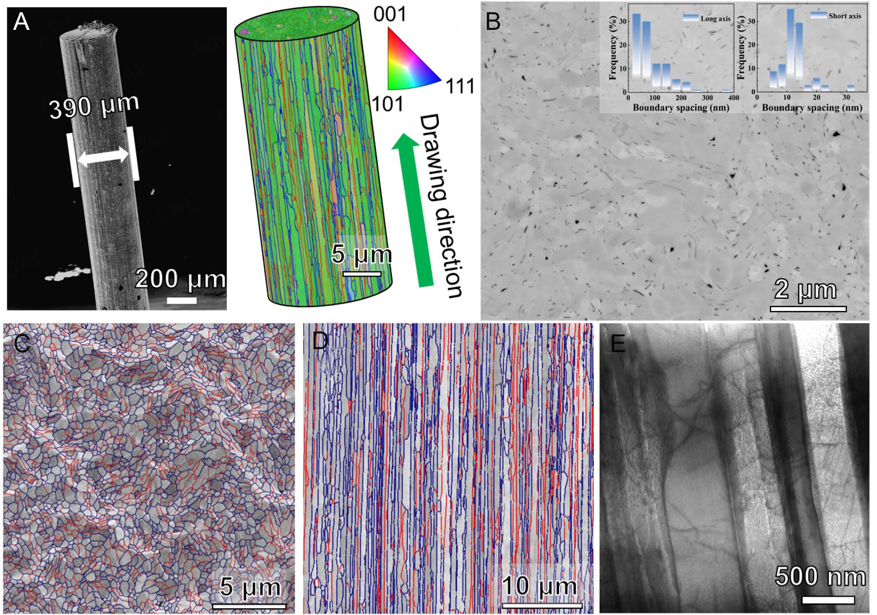
Figure 1. Microstructure of the tungsten wire at ε = 0 (390 μm). (A) SEM micrograph and corresponding illustration (IPF coloring based on the drawing direction) of the sample; (B) BSE image showing the distribution of cerium oxide; (C) Cross-sectional EBSD map, where low-angle grain boundaries (LAGBs, 5°-15°) and high-angle grain boundaries (HAGBs, > 15°) are marked as red and blue lines, respectively; (D) Longitudinal section EBSD map; (E) TEM micrograph showing the fine scale boundary and dislocation structure in a longitudinal section.