

fig7
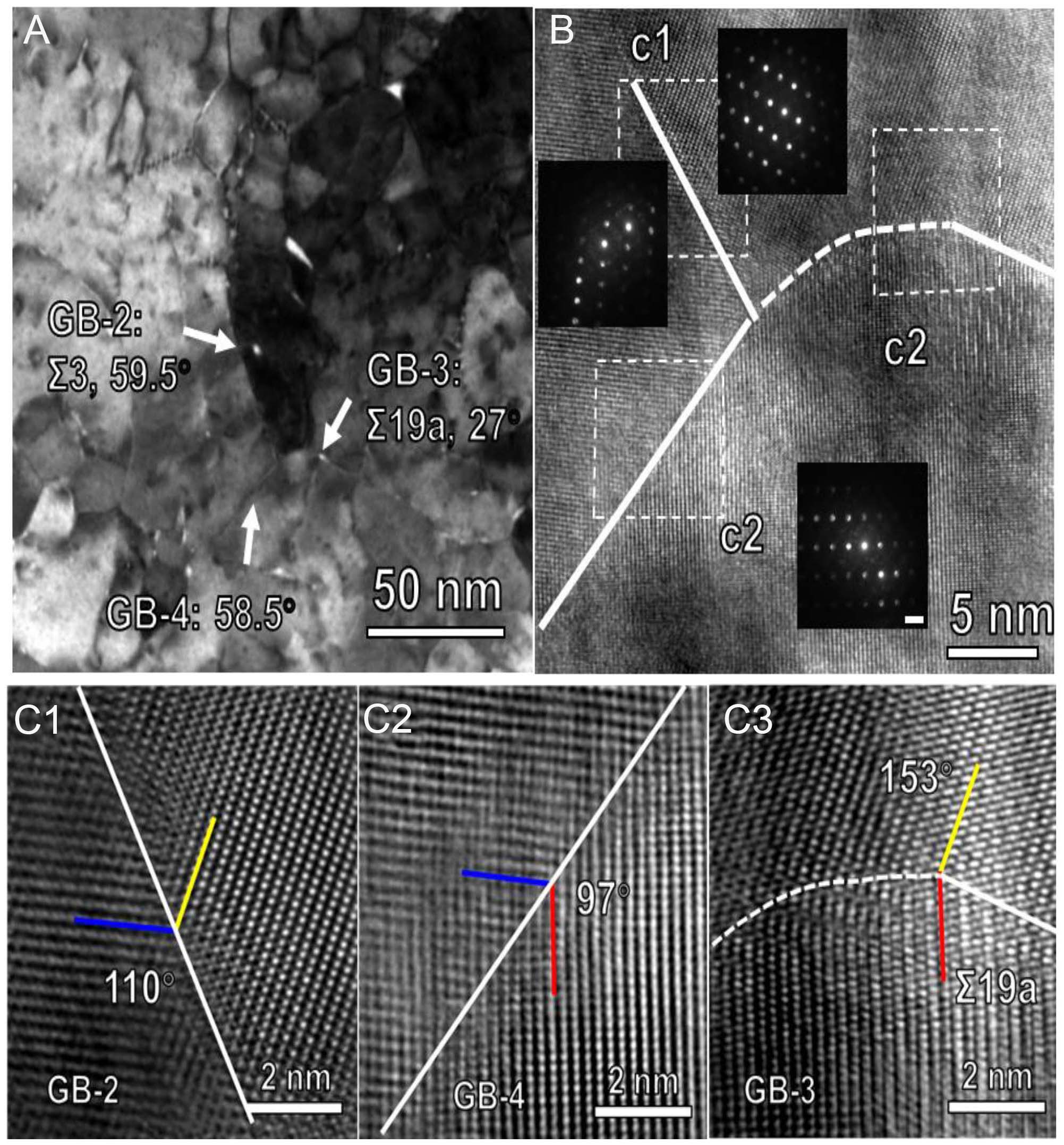
Figure 7. TEM micrographs of the triple junctions marked by white circles in Figure 5C6: (A and B) TEM and HRTEM micrographs of the triple junctions, the NBD patterns show the three grains were observed near to [110]W; (C1-C3) HRTEMs for GB-2, GB-3 and GB-4, respectively. The scale bar for nano beam diffraction patterns is 5 nm-1.