


Tellurium-based materials for nanoelectronics: applications, challenges, and outlooks
 0
0 
Abstract
The realization of high-performance P-type semiconductors remains a central challenge in oxide semiconductors due to the strong localization of holes within oxygen 2p-derived valence bands. This orbital limitation hampers the development of efficient hole conduction pathways, resulting in low hole mobility and poor device characteristics, contrary to the success of N-type oxides such as indium gallium zinc oxide (IGZO) and ZnO. Recently, tellurium-based oxides have emerged as promising candidates to overcome these barriers, offering intrinsic p-type behavior, tunable band structures, and compatibility with low-temperature, back-end-of-line processes. Their unique crystal structures, ranging from helical-chain-derived hexagonal phases based on Te to tetragonal-phase TeOx, enable anisotropic charge transport, reduced non-radiative recombination, and low Schottky barrier heights facilitating efficient hole injection. These advantages have been successfully exploited in P-type field-effect transistors, broadband photodetectors, and multifunctional sensors thanks to the broad spectral absorption, strong electromechanical coupling, and environmental stability of TeOx. This review highlights the material properties of tellurium-based oxides, their device-level performance, challenges, and outlooks for their integration into next-generation nanoelectronic and optoelectronic systems.
Keywords
INTRODUCTION
The development of high-performance p-type semiconductors has long been a major challenge. One key reason lies in the orbital structure of oxide semiconductors: since the valence band is primarily derived from oxygen 2p orbitals, holes tend to be strongly localized, making it difficult to achieve high mobility[1]. This orbital limitation prevents the formation of efficient p-type conduction pathways, leading to poor switching characteristics and high contact resistance. In contrast, n-type oxide semiconductors benefit from the extended nature of the metal cation’s orbitals forming the conduction band, enabling higher mobility and better stability, as demonstrated in commercially viable materials such as indium gallium zinc oxide (IGZO) and ZnO[2]. As a result, realizing reliable p-type oxide channels remains a central challenge in semiconductor research.
To address these limitations, tellurium (Te)-based oxides have recently emerged as promising alternatives, with expanding potential in flexible electronics, transparent circuits, and back-end-of-line (BEOL) compatible processes. This growing interest arises from their low processing temperature (< 400 °C), intrinsic p-type characteristics, excellent environmental stability, and diverse electronic and optical responses[3-5]. Structurally, Te consists of helical chains bound by Van der Waals (VdW) interactions; upon oxidation, it can form hexagonal or tetragonal crystal structures[6-9]. In particular, the hexagonal-symmetry packing of helical Te chains gives rise to a highly anisotropic lattice, enabling direction-dependent charge transport and preferred crystallographic growth directions[10-12]. At reduced dimensions, quantum confinement and control of thickness and diameter further enable band-structure engineering, which is difficult to realize in conventional oxide semiconductors[13-16]. Moreover, because dangling bonds are mainly confined to chain ends, non-radiative recombination is expected to be localized at specific edges, supporting suppressed surface recombination and longer carrier lifetimes[17,18]. Such properties have been successfully exploited in field-effect transistor (FET) fabrication, greatly enhancing their role as p-type semiconductor channels. Te-based FETs, owing to the helical chain-derived hexagonal structure, can form low Schottky barrier heights (SBH) that suppress off-state current and facilitate efficient hole injection[19-23].
In optoelectronics, Te oxides offer broad spectral absorption not only due to their tunable band structures but also because of strong anisotropy and defect-mediated electronic states that extend sensitivity from the visible to the near-infrared (NIR) region[24-28]. This distinguishes them from conventional wide-bandgap oxides such as ZnO or TiO2, which are typically limited to the ultraviolet (UV) regime. These features have enabled the demonstration of broadband photodetectors and integrated imaging platforms, where Te oxides provide both high responsivity and spectral versatility[29-33].
Beyond photodetection, the emergence of non-centrosymmetric Te oxide phases introduces strong electromechanical and thermoelectric coupling. This allows the same material system to function as piezoelectric sensors, strain-gated transistors, and photo-thermoelectric harvesters. Unlike most oxide semiconductors that require separate material platforms for electronic and mechanical sensing, Te oxides combine these responses in a single framework. Such multifunctionality makes them attractive for integrated sensing systems where energy harvesting, environmental detection, and signal processing can be co-localized[34-38].
Historically, Te first attracted interest as a bulk thermoelectric and photoconductive material, where its chiral crystal structure and large coefficient were explored in early infrared detection and energy-harvesting studies. Subsequent advances in chemical synthesis of one-dimensional nanowires and nanotubes enabled better control over morphology and aspect ratio, paving the way for solution-processable Te platforms in flexible thermoelectric and photodetectors. More recently, the discovery of few-layer “tellurene”, together with direct low-temperature growth of 2D Te and amorphous TeOx thin films, has shifted the focus toward transistor- and circuit-level integration, broadband photodetection, and multifunctional sensing. Building on these developments, this review organizes the rapidly expanding Te-based materials landscape from polymorphism and p-type transport mechanisms to transistor technologies, optoelectronic devices, multifunctional sensors, and in-sensor computing, with an emphasis on their prospects for next-generation nanoelectronics.
Taken together, Te-based oxides provide a rare example of a material platform that simultaneously addresses challenges in p-type conduction, broadband optoelectronics, and multifunctional sensing. Nevertheless, important challenges remain in achieving wafer-scale uniformity, controlling interface states, and ensuring compatibility with complex circuit integration. This review will therefore examine the underlying material properties, connect these to device-level functionalities, and outline opportunities for advancing their integration into next-generation semiconductor technologies[39-43].
Tellurium-based devices: from transistors to multifunctional sensors
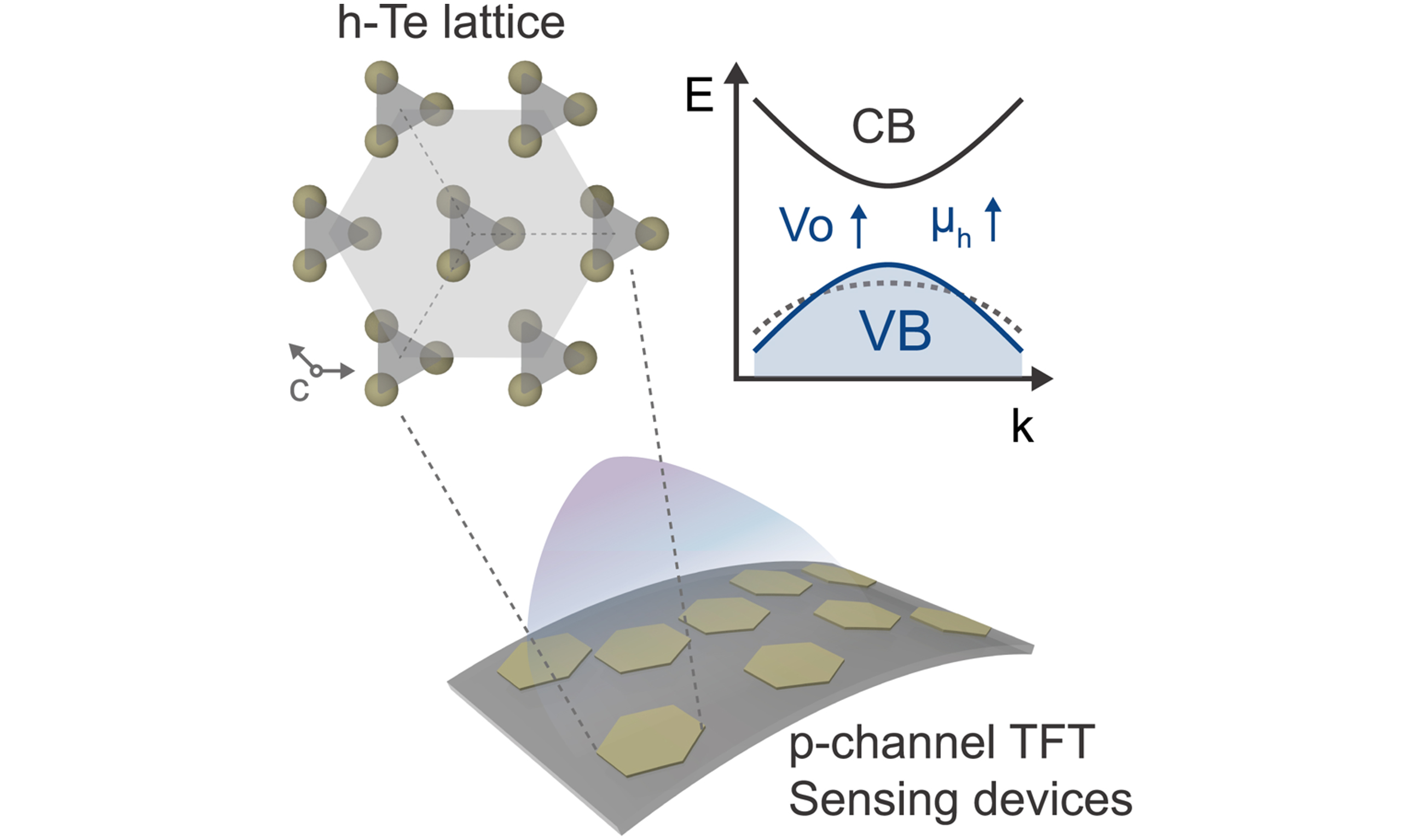
Figure 1 summarizes the diverse application landscape of Te-based electronics and optoelectronics. Owing to its intrinsic p-type transport, high hole mobility, and favorable interfacial chemistry, Te enables the development of crystalline and amorphous p-channel Field Effect Transistors (p-FETs) [Figure 1A]. These devices benefit from low-temperature fabrication, scalability, and ultralow contact resistance, establishing Te as a complementary counterpart to widely used n-type oxide semiconductors[44]. Te based transistors also have been reported to offer enhanced photosensitivity, improved stability, and scalable fabrication[45-46]. In addition, multifunctional sensors fabricated using various Te processes such as nanowire, tubular, heterojunction devices enable dual sensing, photothermoelectric detection, and broadband UV-NIR photodetection[47-50].
Figure 1. Te-based device applications. The central panel illustrates the crystal structure of Te. Adapted from Ref.[18] with permission from Copyright by Wiley-VCH Verlag GmbH & Co. KGaA. (A) p-Channel Transistors: Crystalline and amorphous Te-based FETs with high mobility, scalability, and ultra-low contact barriers[19,44]. Adapted from Ref.[19] and Ref.[44] under the Creative Commons CC BY license(s). (B) Optoelectronic Devices: Plasma-engineered and nanonetwork Te transistors offering enhanced photosensitivity, stability, and scalable fabrication[45,46]. Adapted from Ref.[45] with permission from Wiley-VCH Verlag GmbH & Co. KGaA; and from Ref.[46] under the Creative Commons CC BY license. (C) Multifunctional Sensors: Te nanowire, tubular, and heterojunction devices enabling dual sensing, photothermoelectric detection, and broadband UV-NIR photodetection[47-49]. Adapted from Ref.[49] with permission from Wiley-VCH Verlag GmbH & Co. KGaA; and from Refs.[47,48] under the Creative Commons CC BY license. UV-NIR: Ultraviolet- near-infrared; FET: field-effect transistor; PI: polyimide; p-FETs: p-channel FETs; NMs: nanomeshs.
In parallel, the Te nanostructure provides rich opportunities for optoelectronic devices [Figure 1B]. Plasma-engineered thin films and nanonetworks exhibit improved crystallinity and enhanced photosensitivity, while Te semiconductor heterojunctions extend the spectral response from the UV to the NIR. The broadband light absorption of Te, influenced by its surface passivation due to VdW bonding, translates into high responsivity, low noise, and reliable operation suitable for integrated imaging and sensing platforms[39,47,51].
Beyond logic and photodetection, Te structural chirality and coupled thermoelectric-piezoelectric effects enable the realization of multifunctional sensors [Figure 1C]. Sensing functionalities such as nanowire bimodal tactile sensors, self-rolled tubular photo-thermoelectric detectors, and heterojunction-based self-powered photodiodes highlight how Te nanostructures can simultaneously transduce optical, thermal, mechanical, and chemical stimuli. These multifunctional capabilities point toward next-generation wearable electronics, immersive virtual/augmented reality interfaces, and environmental monitoring systems[48,51].
Collectively, Figure 1 illustrates how the distinctive materials attributes of electronic anisotropy, scalable low-temperature processing, and versatile physical responses are being translated into a broad portfolio of emerging devices spanning transistors, optoelectronics, and multifunctional sensing technologies.
STRUCTURES AND PHASE BEHAVIOR OF TELLURIUM-BASED MATERIALS
Polymorphism in tellurium-based materials
Before discussing Te applications in electronics, the origin of hexagonal structures in Te will be addressed. According to the dimension of Te, the equilibrium phase can vary, ranging from nanoflake types, bulk trigonal phase, amorphous phase, to tetragonal phase. At each phase, Te shows different electrical conductivity common in P-type characteristics [Figure 2]. Especially, the bulk trigonal Te is characterized by a helical chain bonded with VdW interaction arranged in a hexagonal array. These weakly bonded helical chains do not have crystal symmetry, but they show chiral structures. This chirality endows Te with diverse physical properties, including electrical magneto-chiral anisotropy, spin polarization, and bulk photovoltaic effect[52], within a highly crystalline hexagonal array. Although chirality is common in organic materials, the chiral structure of hexagonal Te enables its wide use in robust spintronic and optoelectronic applications.
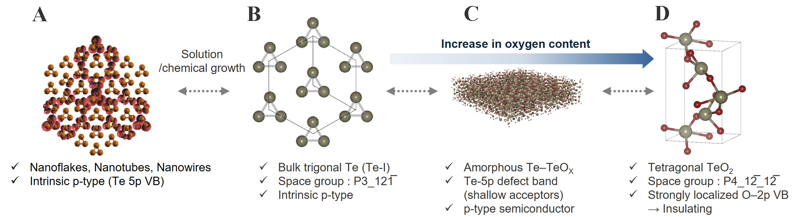
Figure 2. Structural evolution of Te depending on the synthesis conditions and oxidation state[18]. (A) Te nanostructures. Adapted from Ref.[18] with permission from Copyright by Wiley-VCH Verlag GmbH & Co. KGaA; (B) Bulk trigonal Te; (C) Amorphous Te-TeOx; (D) Tetragonal TeO2 (rendered using VESTA).
However, the low bonding dissociation energy (BDE) of Te (~259.8 kJ mol-1) due to the weak VdW bonding among the individual helical chains makes the Te easily oxidized at room temperature[53]. Furthermore, partial oxidation at the Te surface accelerates the change of valency of Te ion from Te4+ to Te6+[54]. Thus, as the amount of oxygen incorporation increases, phase transformation in Te can be facilitated according to the following sequence: 1) trigonal Te → 2) amorphous-TeO2 → 3) amorphous-TeOx → 4) tetragonal TeOx. This transition finally results in an insulating electronic phase. This is why the passivation layer is imperative when applying Te as a semiconducting layer in electronic devices[22,55-57].
Origin of P-type character in tellurium-based materials
Typically, Te-based materials show p-type conduction properties in every phase. The common nature in p-type conduction may be attributed to the orbital shape of Te valence electrons, which is 5p. Since the partially filled 5p orbital in Te {[He]5s25p4} facilitates hole formation and operates as a shallow acceptor, trigonal-phase Te shows p-type characters. However, if the crystallinity collapses due to Te oxidation, p-type conductivity can increase. This can be explained by two factors: (1) hybridization between Te 5p and O 2p orbitals shifts the valence band maximum (VBM) upward[19], and (2) orbital-overlap pathways between Te and O become more diverse owing to random orientation in the amorphous phase [Figure 3A-C]. Therefore, localized states are formed near the VBM, facilitating active hole hopping in this region [Figure 3D].
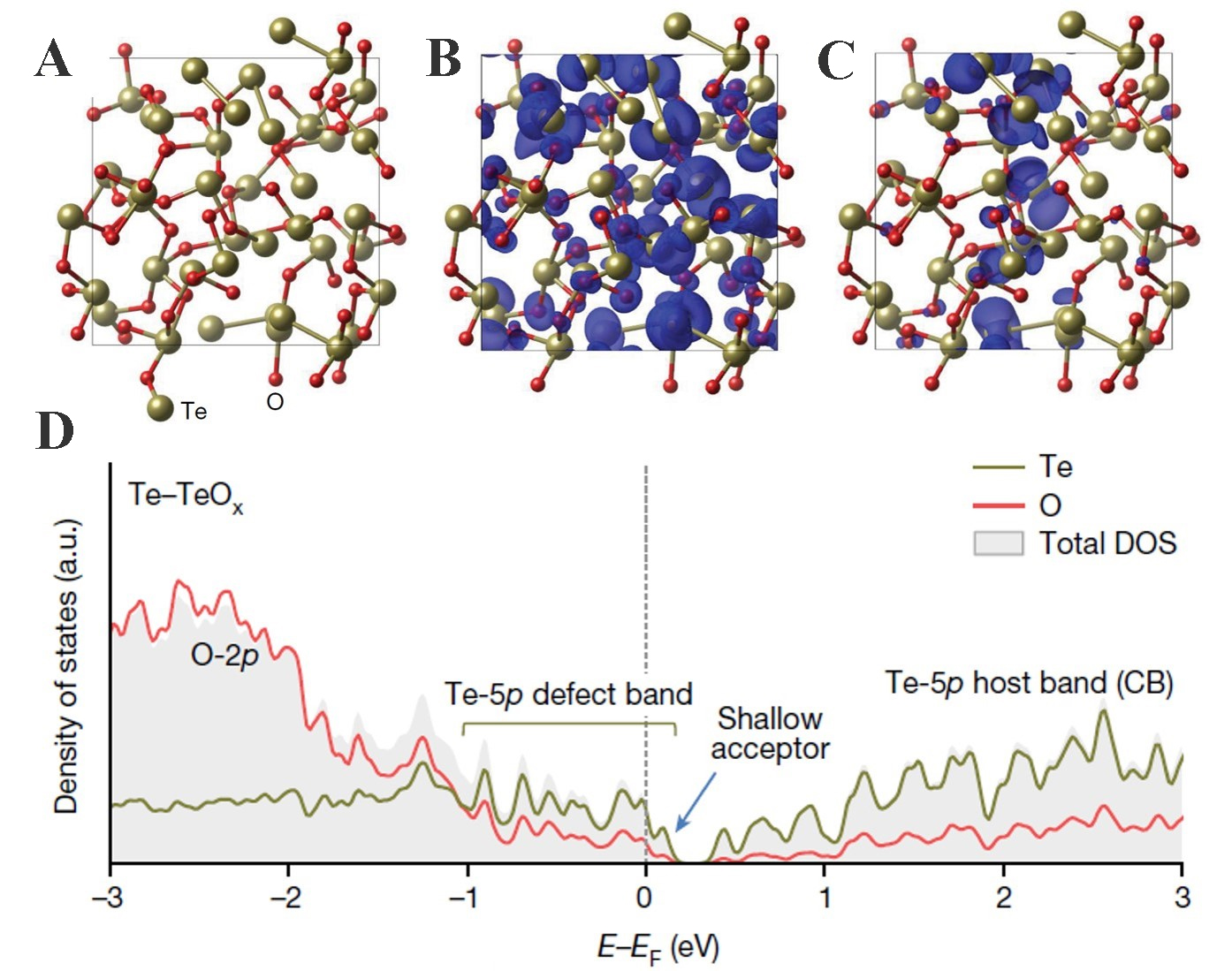
Figure 3. Atomic and electronic structures of amorphous Te-TeOx. (A) Atomic configuration of amorphous Te-TeOx generated by DFT simulations; (B) Charge density distribution of the Te-5p defect band, showing the spatially dispersed and percolated Te-5p orbitals; (C) Charge density distribution of the shallow acceptor state near the Te-5p defect band; (D) Projected density of states (DOS) of Te-TeOx calculated by DFT-PBE, highlighting the O-2p states, Te-5p defect band, and shallow acceptor levels near the Fermi energy (EF)[19]. (A-D) Adapted from Ref.[19] under the Creative Commons CC-BY license. DFT-PBE: density functional theory - Perdew-Burke-Ernzerhof.
DEVICE APPLICATION OF TELLURIUM-BASED MATERIALS
P-type FET using tellurium-based materials
This section reviews the performance of Te-based p-type FETs enabled by a range of Te synthesis routes. Reported Te synthesis methods include solution processes, chemical vapor deposition (CVD), physical vapor deposition (PVD), thermal evaporation, and UV/O3 treatment. Here, we review the device performance of Te-based FETs fabricated by CVD, thermal evaporation, and UV/O3 treatment, along with the reliability of logic circuits built from them[58]. It has been reported that, during deposition, the carrier mobility and grain size of Te can be tuned by substrate temperature and deposition rate[59]. Although early Te devices generally showed modest switching characteristics, thermally evaporated Te thin films exhibit high mobility while keeping the process simple even at wafer scale, enabling NAND (NOT AND) logic and co-integration with other process flows[60,61].
The electrical characteristics of disordered tellurium oxide (DTO)-based p-type transistors are highly sensitive to ambient conditions and thermal processing, as illustrated in Figure 4. In the air/vacuum comparison [Figure 4A], oxygen adsorption/desorption plays a key role in modulating channel carrier density[58]. Measurements in ambient air show a pronounced hysteresis and enhanced p-doping behavior, originating from oxygen molecules that trap electrons and consequently increase the hole concentration at the surface. In contrast, vacuum measurements suppress adsorbate-related charge trapping, yielding a reduced hysteresis window and more ideal transfer curves. Such environment-dependent behavior highlights the inherent surface-chemistry-driven reconfigurability of DTO, enabling mode switching between logic operation and synaptic functionality. The influence of annealing temperature [Figure 4B] further demonstrates that mild thermal treatment, particularly around 150 °C, optimizes device performance and leads to the highest hole mobility and on/off ratio among the tested conditions[58]. This enhancement is attributed to partial structural relaxation, trap reduction, and improved carrier transport pathways within the disordered Te-oxide network. Notably, the ability to improve performance via low-temperature processing offers a compelling advantage for complementary metal-oxide semiconductor (CMOS)-compatible oxide electronics and large-area fabrication. In addition, CMOS logic demonstrations [Figure 4C and D] show that DTO p-FETs can be monolithically integrated with n-type In2O3 to realize NAND and NOR (NOT-OR) logic gates[58]. The output logic states match the Boolean truth table across different input voltage combinations, indicating that DTO is not limited to neuromorphic operation but can also function as an active building block in conventional logic circuitry. This duality underscores DTO as a rare single-material system capable of bidirectional operation, transitioning between transistor mode and neuromorphic mode depending on surface oxygen dynamics, and positions it as a promising platform for reconfigurable oxide-based electronics.
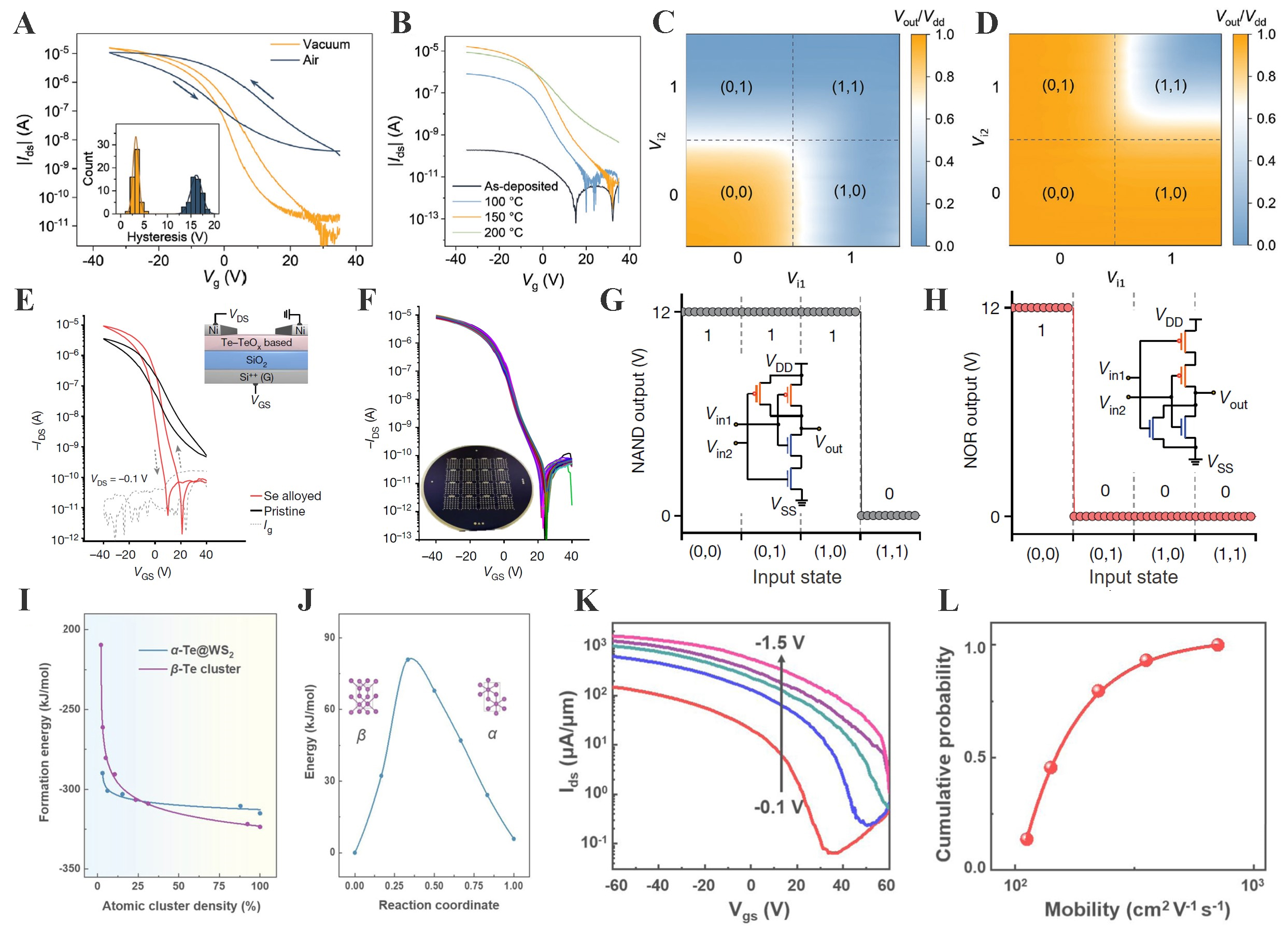
Figure 4. Device stability, logic operation, phase engineering, and transport characteristics in Te-based transistors. (A) Transfer curves of FETs measured in vacuum and air, showing mode change driven by oxygen adsorption; (B) Transfer characteristics after thermal annealing at different temperatures, indicating improved switching behavior; (C) NAND logic output map demonstrating correct low-output at (1,1); (D) NOR logic output map showing high output only at (0,0)[58]; (A-D) Adapted from Ref.[58] with permission from Wiley-VCH Verlag GmbH & Co. KGaA. (E) Transfer curves of pristine and Se-alloyed Te-TeOx TFTs, showing reduced onset voltage and suppressed leakage; (F) Transfer curves of 80 Se-alloyed Te-TeOx TFTs, highlighting wafer-scale uniformity; (G) Output characteristics of a complementary NAND gate combining p-channel Te-TeOx and n-channel In2O3 TFTs; (H) NOR gate characteristics from the same complementary TFTs, showing correct logic operation[19]; (E-H) Adapted from Ref.[19] under the Creative Commons CC-BY license. (I) Formation energy of α- and β-Te as a function of atomic cluster density on WS2, indicating α-phase favored at low density and β-phase at high density; (J) Calculated transition barrier between α- and β-phases; (K) Transfer curves of β-Te FETs under various drain biases; (L) Cumulative mobility distribution of β-Te devices[44]. (I-L) Adapted from Ref.[44] under the Creative Commons CC BY license. FET: Field-effect transistor; NAND: NOT AND; TFT: thin film transistor.
Another approach alloys Te-TeOx with Se to form the semiconductor channel. Selenium does not perturb the nanoscale morphology but is used to enhance electrical properties[62]. The optimal composition was determined to be Se-Te3, showing typical p-channel behavior with a mobility of 4.2 cm2 V-1 s-1 and an on/off ratio of ~104 [Figure 4E][19]. At higher Se contents, a pronounced n-doping effect appears and the thin film transistor (TFT) performance degrades. Constant-bias stress tests were carried out to assess operational stability; the change of threshold-voltage (ΔVth) was observed as 3.2 V and 3.4 V under positive and negative stress, respectively, after 5,400 sec. For uniformity and reliability, wafer-scale processing of the Se-alloyed Te-TeOx semiconductor was performed; the resulting arrays showed superior device uniformity and reproducibility [Figure 4F][19]. In the previous devices, compatibility with established n-type Field Effect Transistors (n-FETs) was confirmed by integrating NAND and NOR gates; the inverter achieved a high voltage gain of 1,300 at VDD = 20 V, and each NAND and NOR gate produced the correct output in response to the given input [Figure 4G and H][19]. Evaporated Te-TeOx-Se thin films, single-crystalline SexTe1-x alloys grown by precursor-confined CVD have recently pushed the performance of Te-based p-type transistors. Huang et al. synthesized 2D SexTe1-x nanosheets with tunable Se content (x up to ≈ 0.49), and optimized a Se0.30Te0.70 channel that delivered an on/off current ratio of 4 × 10⁵ and a room-temperature hole mobility of 120 cm2 V-1 s-1, far surpassing thermally evaporated SexTe1-x films with similar composition. By monolithically integrating the Se0.30Te0.70 p-channel with an n-type MoS2 transistor, they further demonstrated a 2D CMOS inverter with a gain of ~30 at VDD = 3 V[63].
Efforts have been made to elucidate the phase formation mechanism during single-crystalline Te growth and to understand how synthesis conditions influence its charge transport behavior. As shown in Figure 4I, the formation energies of both α-Te and β-Te clusters on WS2 decrease significantly with increasing cluster density, suggesting enhanced thermodynamic stability at higher coverage[44]. Notably, β-Te exhibits slightly lower formation energy in the low-density regime than α-Te, implying that β-phase nuclei may preferentially form during the initial growth stage. The reaction pathway in Figure 4J further reveals an energy barrier for the β → α transition, indicating that thermal activation is required for phase conversion and that phase selectivity can be influenced by growth conditions[44]. Electrical characterization [Figure 4K] confirms that exfoliated Te devices exhibit clear p-type behavior, showing increased hole current under more negative gate bias[44]. The threshold voltage (Vth) shift from -0.1 V to -1.5 V under different gate conditions suggests tunable carrier injection governed by interfacial energy states and trap distributions. The cumulative mobility distribution [Figure 4L] is mainly concentrated in the range of 102-103 cm2 V-1 s-1, highlighting the intrinsically high mobility and good device-to-device reproducibility of Te channels[44]. Collectively, these findings demonstrate the strong potential of Te as a high-performance channel material for next-generation flexible electronics.
Meanwhile, several works have also pursued different approaches to tune Te characteristics and improve device operation. Low-temperature evaporated Te films have achieved high mobility, mechanical robustness, and even basic CMOS logic demonstration when integrated with amorphous IGZO (a-IGZO)[20]. In parallel, UV/O3-induced oxidation yields amorphous TeOx channels with reduced off-current and lower contact barriers, enabling improved switching behavior and tunable transport mechanisms[56]. Collectively, these routes represent versatile strategies toward realizing p-type Te devices and suggest strong compatibility with a-IGZO n-FETs for future CMOS-level integration.
The following device is fabricated by depositing Te nanostructures at room temperature via sputtering and then performing post-deposition annealing (PDA), followed by Al2O3 encapsulation to enhance the hexagonal thin-film crystallinity of Te. A key feature of this process is PDA carried out below 200 °C, which oxidizes Te and increases the Te4+ fraction, thereby widening the bandgap and increasing the hole concentration. Subsequent Al2O3 encapsulation enlarges the grain size and improves crystallinity, leading to performance gains in terms of mobility and on/off ratio[64,65].
To validate the performance of devices produced by this process, 70 devices were randomly selected from a 4-inch wafer-scale batch, and mobility, subthreshold swing (SS), on/off ratio, and Vth were measured [Figure 5A][22]. All metrics were clustered around their medians, confirming good uniformity. To demonstrate that the device is applicable for CMOS, a p-type Te FET is complemented with n-type IGZO FETs. This CMOS device shows a typical rail-to-rail swing and high gain at low input voltages, showing that this device is also effective at the circuit level when integrated with the IGZO FET [Figure 5B and C][22].
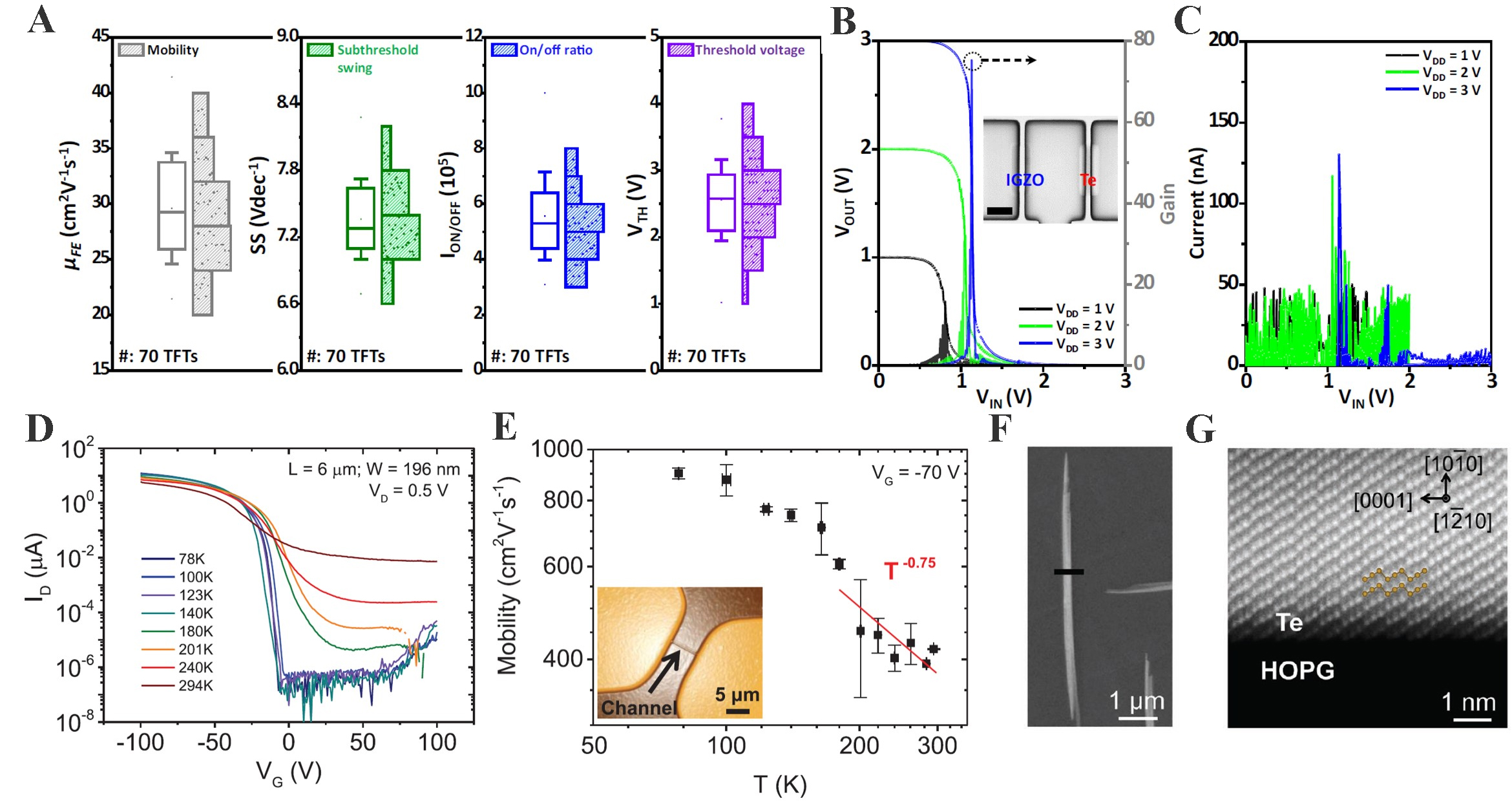
Figure 5. Device statistics, CMOS inverter operation, and temperature-dependent transport in Te-based transistors. (A) Statistical distribution of field-effect mobility (µFE), subthreshold swing (SS), on/off ratio (ION/IOFF), and threshold voltage (Vth) extracted from 70 Te-based transistors; (B) Voltage transfer curves and corresponding gain of a CMOS inverter composed of IGZO n-channel and Te p-channel transistors at VDD = 1-3 V (inset: optical micrograph, scale bar, 2 µm); (C) Static current characteristics of the CMOS inverter under different VDD values[22]; (A-C) Adapted from Ref.[22] under the Creative Commons CC BY license. (D) Transfer curves (Ids - Vgs) of Te-based transistors measured from 78 K to 294 K (L = 6 µm, W = 196 nm, VD = 0.5 V); (E) Temperature-dependent mobility following a phonon-limited T-0.75 relation (inset: optical image of the transistor channel, scale bar, 5 µm); (F) SEM image of needle-like Te nanostructures grown on HOPG (scale bar, 1 µm); (G) Atomically resolved STEM image of the Te/HOPG interface along [0001], revealing the helical chain structure (scale bar, 1 nm)[21]; (D-G) Adapted from Ref.[21] with permission from Wiley-VCH Verlag GmbH & Co. KGaA. CMOS: Complementary metal-oxide semiconductor; IGZO: indium gallium zinc oxide; HOPG: highly oriented pyrolytic graphite; STEM: scanning transmission electron microscopy; SEM: scanning electron microscope.
Another Te-based FET fabrication process involves epitaxial growth of Te without transfer or exfoliation under 120 ℃; this p-FET achieves an unprecedented room-temperature hole mobility approaching 707 cm2 V-1 s-1. Interestingly, epitaxially grown Te on a highly oriented pyrolytic graphite (HOPG) substrate shows improved SS and reduced off current as temperature decreases [Figure 5D][21]. Also, the increased field-effect mobility by the temperature decrease in the epitaxially-grown Te FET indicates that phonon scattering is dominant at low-temperature region [Figure 5E][21]. Furthermore, in the high-temperature regime (T ≥ 170 K), the temperature-dependent mobility follows a power-law behavior (μ ∝ T-α) with an exponent α = 0.37, suggesting that the mobility is limited by phonon scattering. While pure acoustic phonon scattering typically leads to α ≈ 1, the observed sublinear behavior (α < 1) is consistent with reports on other 2D materials such as MoS2 and black phosphorus. This behavior is likely attributed to the quenching of homopolar phonon modes or weakened electron-phonon coupling. Devices grown by this method exhibit dense needle-like structures, implying few grain boundaries [Figure 5F]. In this nanostructure, helical chains composed of a hexagonal lattice are observed through scanning transmission electron microscopy (STEM) in which the chains are deposited on HOPG substrate via VdW bonding [Figure 5G]. This microstructure suggests that the epitaxially grown Te chains can bond not only with the HOPG substrate but also with other substrates, influenced by VdW interactions[20].
Such a low-temperature growth process for the highly crystalline Te film is regarded as essential for future research on highly integrated monolithic 3D (M3D) circuit design, suggesting strong suitability for both flexible processing and M3D fabrication[21].
Optoelectrical performances using tellurium-based materials
This section reviews the performance and characteristics of Te-based FETs for the optoelectronic functionalities. Owing to the 5p orbital nature in Te, acceptor energy states located at the VBM enable high hole mobility and strong optical absorption. In addition, the phase of Te can be tuned by processing, allowing bandgap engineering; as a result, Te is suitable for wide-wavelength light absorption and for realizing low-noise FETs. Because the Te film tends to bond with the substrate via VdW interactions, the VdW gap between the substrate and the Te film reduces the SBH and enables high photosensitivity[18,24,66-68].
One study on Te-based optoelectronic devices involves an Ar plasma-treated Te device. This treatment is to enhance Te film crystallinity, planarize the surface, and consequently increase the hole concentration by offsetting fermi Energy (Ef) toward the VBM. This shifted Ef by Ar plasma treatment creates sub-gap states and enables high photo detectivity. FETs fabricated by this process exhibit better switching performance than pristine Te-based devices under the same Vgs [Figure 6A][45]. This enhancement is attributed to not only higher hole concentration but also suppression of electron transport due to larger SBH [Figure 6B][45]. This suppression of electrons induces a reduction in off current, making a higher on/off current ratio. In addition, the drain-source current (Ids) increases progressively with optical intensity, indicating that the increased injected optical energy induces a photogating effect and high photosensitivity [Figure 6C][45]. As shown in Figure 6D, the plasma-treated Te phototransistor exhibits an exceptionally high detectivity, which is nearly an order of magnitude higher than the pristine device[45]. This enhancement originates from the plasma-induced subgap states near the valence band, enabling an efficient trap-assisted photogating effect. Meanwhile, detectivity decreases with increasing power density due to trap saturation.
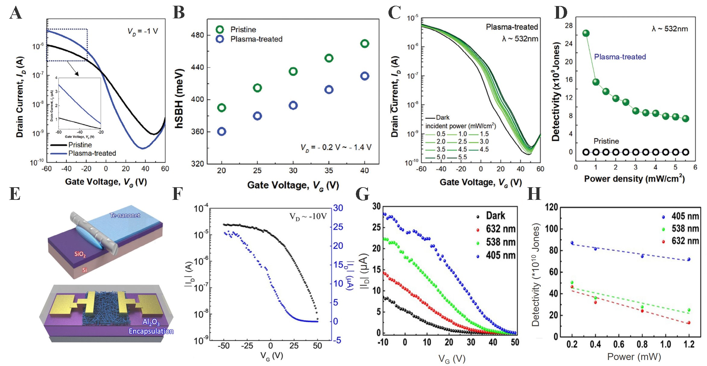
Figure 6. Electrical and optoelectronic properties of plasma-treated TeFETs and Te-nanonetwork transistors. (A) Transfer curves of pristine vs. plasma-treated TeFETs, showing enhanced on-current and suppressed off-current; (B) Extracted hole Schottky barrier height, reduced after plasma treatment; (C) Transfer characteristics under 532 nm illumination with varying power densities, highlighting increased photocurrent; (D) Detectivity as a function of optical power, demonstrating superior photodetection in plasma-treated devices[45]; (A-D) Adapted from Ref.[45] with permission from Wiley-VCH Verlag GmbH & Co. KGaA. (E) Schematic of Te-nanonetwork transistor with Al2O3 encapsulation; (F) Transfer curves in the dark, showing stable p-type behavior with high on/off ratio; (G) Wavelength-dependent photoresponse under 405, 538, and 632 nm illumination; (H) Detectivity versus optical power at different wavelengths, confirming wavelength-sensitive photodetection[46]. (E-H) Adapted from Ref.[46] under the Creative Commons CC BY license. FET: Field-effect transistor.
Phototransistors fabricated via a low-temperature solution process also demonstrate excellent performance uniformity at the wafer scale. In this route, a solution-synthesized Te nanonetwork is bar-coated on a SiO2 substrate, dried, and then encapsulated with Al2O3 to reduce trap density and hysteresis [Figure 6E][46]. From the current-voltage (I-V) curves and the spectral photo response, the devices exhibit a stronger photogating effect at shorter wavelengths, i.e., higher responsivity for shorter-wavelength illumination [Figure 6F and G][46]. Moreover, across all wavelengths, lower incident power yields better detectivity; the derived detection-limit curves benchmark the limits as a function of light source and power[46]. As shown in Figure 6H, the Te-nanonetwork phototransistor shows a wavelength-dependent detectivity, reaching up to 8.7 × 10¹¹ Jones under blue light (405 nm) illumination, which is significantly higher than that under green (538 nm) and red (632 nm) light[46]. The detectivity decreases with increasing incident power due to trap-state saturation. These results suggest the strong wavelength selectivity and high sensitivity of the low-temperature-processed Te-nanonetwork phototransistor, particularly in the short-wavelength visible region. Te-Se alloying has also been explored in amorphous thin-film photodetectors to combine broadband absorption with wafer-scale processability. Chen et al. used room-temperature pulsed-laser deposition to prepare 2-inch-scale amorphous Te0.65Se0.35 nanofilms with a Hall mobility of 20.5 cm2 V-1 s-1 and high thickness uniformity, and realized photodetectors with a broadband spectral response from 405 nm to 1,550 nm. Under 635 nm illumination, the devices achieved a responsivity of 7.35 A W-1, External Quantum Efficiency (EQE) of 1,440%, and detectivity of 1.32 × 10⁹ Jones. These results demonstrate that amorphous Te-Se alloys can serve as scalable, mechanically robust platforms for broadband optoelectronics. This work shows that amorphous Te-Se alloys can combine large-area processability with broadband optoelectronic functionality, complementing crystalline Te-based photodetectors[69].
Common to both device types, the low-temperature processes target flexible applications, and the devices operate at low voltages, resulting in optimized noise performance.
Sensing performances using tellurium-based materials
Te-based FETs exhibit multiple phases arising from their intrinsic material characteristics and display distinct thermal and polarization responses. Consequently, they are well-suited for self-operating optical/thermoelectric functionalities that can be operable only by light absorption without input bias. Owing to the VdW bonding that stabilizes Te hexagonal structure, phase changes can be induced by lattice strain originating from the heat or piezoelectric effects. In this section, we review these aspects.
Te-based FETs are highly sensitive to lattice deformation induced by thermal or piezoelectric stimuli, owing to their intrinsic phase-transition characteristics. Phase transitions modify the electronic band structure, carrier separation efficiency, and interfacial bonding states, thereby regulating overall optoelectronic performance. Consequently, Te devices exhibit strong potential for self-operating optical and thermoelectric functionalities that can be actively tuned by external perturbations such as light, heat, and piezoelectric effects[70-72].
By exploiting the anisotropic electronic structure of Te, originating from its helical 1D chain crystal lattice, a sensor capable of simultaneously measuring piezoelectric and thermoelectric signals without crosstalk can be realized using a Te nanowire array. This functionality arises because the intrinsic anisotropy of Te induces directional polarization, which decouples piezoelectric resistance changes from thermoelectric voltage shifts, allowing simultaneous signal readout without interference[48,73,74]. The Te array device [Figure 7A] under temperature and pressure stimuli characterizes the l polarization direction of the Te. By this polarization direction, the change of resistance can be shown with the distinct electrical responses [Figure 7B][25-27]. Accordingly, temperature stimuli are read out as voltage, and in the composite circuit, the concurrently acquired changes in resistance and voltage enable wafer-scale uniform device fabrication and fast response thanks to the high hole mobility of the nanowires [Figure 7A][48]. When a thermal stimulus is applied, a threshold-voltage (Vt) shift appears, whereas under a pressure stimulus, the slope of the I-V curve remains constant, evidencing that the voltage readout is insensitive to stress [Figure 7B][48]. These results resolve the crosstalk issue common to conventional sensors and suggest scalability to flexible systems.
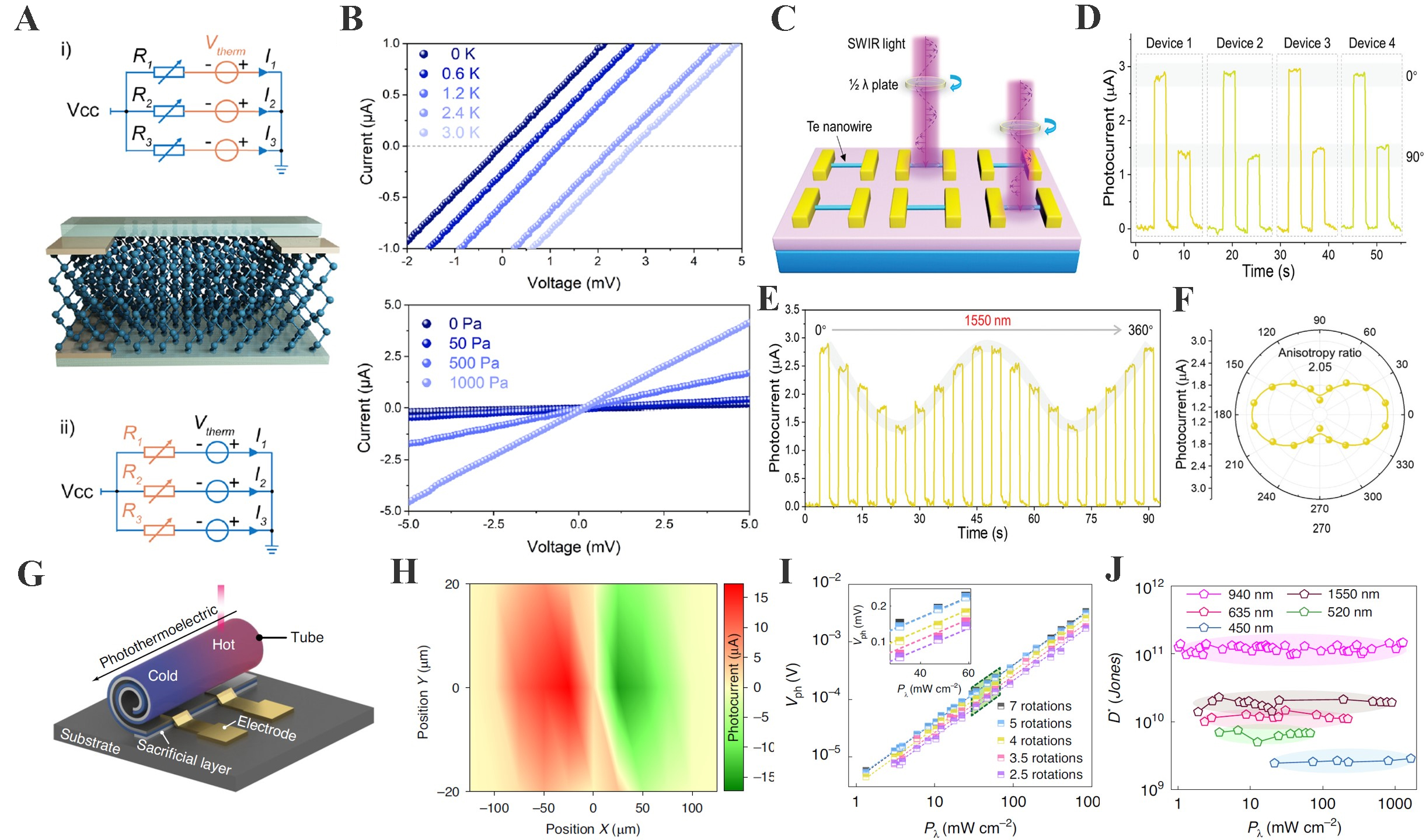
Figure 7. Multifunctional Te-based sensors and photodetectors. (A) Working principle and equivalent circuits of Te nanowire-based bimodal tactile sensors under thermal and pressure stimuli; (B) I-V curves showing thermoelectric response at low temperatures (top) and piezoresistive behavior under applied pressures (bottom)[48]; (A and B) Adapted from Ref.[48] under the Creative Commons CC BY license. (C) Polarization-dependent SWIR measurement setup using a half-wave plate and aligned Te nanowires; (D) Photocurrent of four devices under 1,550 nm illumination at 0°/90° polarization; (E) Time-resolved response during continuous polarization rotation (0-360°); (F) Polar plot confirming anisotropic photocurrent behavior[49]; (C and D) Adapted from Ref.[49] with permission from Wiley-VCH Verlag GmbH & Co. KGaA. (G) Schematic of a self-rolled Te tubular photothermoelectric detector; (H) Spatial photocurrent mapping at 940 nm, showing geometry-dependent response; (I) Photovoltage versus incident power for different rolling rotations, exhibiting linear scaling; (J) Detectivity across multiple wavelengths (450-1,550 nm), demonstrating broadband high-sensitivity performance[47]. Adapted from Ref.[47] under the Creative Commons CC BY license. I-V: Current-voltage; SWIR: short-wave infrared.
To provide a more detailed understanding of the polarization-resolved behavior, Figure 7C schematically depicts the optical measurement configuration, where a 1,550 nm short-wave infrared (SWIR) beam is incident onto the Te nanowire array while a half-wave plate is used to continuously adjust the polarization direction[49]. This setup allows direct correlation between the angle of the incident electric field and the resulting photocurrent. The individual device responses are summarized in Figure 7D, showing four separate channels measured under orthogonal polarization states (0°/90°)[49]. Notably, all devices produce nearly identical switching behavior, confirming that the epitaxial alignment ensures minimal variation across the array and enabling scalable detector integration. A dynamic polarization sweep is shown in Figure 7E[49]. As the polarization angle is rotated through a full 360°, the output photocurrent exhibits periodic modulation with well-defined maxima and minima. This reversible oscillation reflects the directional absorption along the nanowire axis, demonstrating a reliable angular response without noticeable degradation across repeated cycles. The extracted angular photocurrent distribution is visualized in Figure 7F through a polar representation, where a clear elliptical profile highlights the anisotropic nature of the Te nanowire photodetectors[49]. The degree of intensity contrast between the major and minor axes indicates pronounced polarization discrimination, supporting the feasibility of Te nanowires as SWIR-active polarization sensing components that can complement conventional broadband detectors. Beyond polarization sensing, 2D Te integrated with n-Si has also been utilized to realize a self-driven broadband photodetector based on a Te/Si heterojunction. The built-in electric field enables photocarrier separation at zero bias, and the broadband response is mainly governed by the Te/Si interface, where Si absorbs up to ~1,100 nm while Te maintains strong absorption and high mobility into the NIR region[51,75-77]. This structure therefore expands detection wavelength while preserving low-power operation, highlighting the versatility of Te in both polarization-resolved and broadband photodetection platforms.
To transcend the limitations of planar photodetectors (PTE), a 3D PTE architecture formed by self-rolling is also available. This approach leverages localized optical energy to markedly boost the self-driven photovoltage [Figure 7G][47]. In this rolled-up geometry, light confinement enhances the local field intensity, and the winding number and tube diameter tune both wavelength selectivity and sensitivity by modulating the spatial distribution of confined optical fields. Because energy localization varies with position in the 3D tube geometry, the photocurrent magnitude can be controlled solely by the laser spot position, as shown by photocurrent maps scanned along the tube’s x and y directions [Figure 7H][47]. Moreover, wavelength selectivity and sensitivity can be tuned by the number of windings, tube diameter, and wall thickness: the slope of the Vph (photovoltage) - Pλ (incident power density) straight line increases with the number of windings, and mapping across multiple wavelengths confirms the dependence on winding count and diameter [Figure 7I and J][47]. In addition, recent work has demonstrated that 2D Te can function as a high-performance flexible temperature-sensing material. Using an isolated plasma soft deposition (IPSD) process, wafer-scale 2D Te films were fabricated on Si and Polyethylene terephthalate (PET) substrates, exhibiting a hole mobility of 103 cm2 V-1 s-1 and a bending radius of 12 mm. The films also showed stable thermoresistive responses maintained under repeated bending and long-term operation, indicating that Te can support reliable wearable thermal sensors as well as multifunctional tactile platforms. These results demonstrate that the strong temperature dependence of transport in low-dimensional Te can be exploited as an additional sensing degree of freedom in integrated systems[78].
In-sensor computing using tellurium-based materials
Research has also been conducted on combining a Te-based 2D channel with a ferroelectric to realize a memristor memory[28,30,31]. In this device, electrical pulses induce long-term memory, while optical pulses induce short-term memory; applying this to operations in the optical-communication band enables both photosensing and memory within a single device. The stack is fabricated in the order: bottom Au gate → CulnP2S6 (CIPS) → hexagonal Boron Nitride (h-BN) → Te channel [Figure 8A][35]. The CIPS layer non-volatily fixes hole accumulation/depletion in the Te channel, forming long-term memory under electrical pulsing. Photogenerated Electron Hole Pairs (EHPs) in Te under optical pulsing accumulate near the h-BN interface and trigger a transient polarization in CIPS, which acts as short-term memory [Figure 8B][35]. This short-term memory originates from transient screening of the ferroelectric polarization, where photogenerated carriers in Te temporarily modulate the CIPS dipoles without producing a stable polarization reversal. These characteristics align with reservoir computing (RC), where inputs are fixed and only the readout layer is trained; as a result, high performance can be achieved with few trainable weights, greatly reducing the cost/power of real-time learning [Figure 8C][35]. Likewise, the device’s short-term memory yields time-dependent mapping into distinct high-dimensional representations, demonstrating that multi-bit functionality can be realized with a simplified readout layer [Figure 8D][35]. In the context of RC, the fading memory behavior of the device provides the temporal dynamics, while the nonlinear polarization response of the ferroelectric-semiconductor interface enables high-dimensional mapping of input signals.
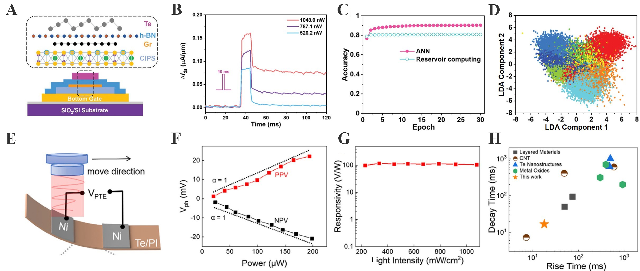
Figure 8. In-sensor memory and photothermoelectric performance of Te-based devices. (A) Schematic of the Te/h-BN/graphene/CIPS van der Waals heterostructure memory device on SiO2/Si; (B) Channel conductance modulation (ΔIds) under 1,550-nm optical pulses at different powers, showing short-term potentiation; (C) Recognition accuracy for handwritten digits using ANN and reservoir computing frameworks; (D) LDA plots of reservoir outputs, illustrating well-clustered feature distributions[35]; (A-D) Adapted from Ref.[35] with permission from Copyright by Wiley-VCH Verlag GmbH & Co. KGaA. (E) Schematic of the flexible Te nanomesh photothermoelectric detector, where laser illumination induces position-dependent V_PTE; (F) Photovoltage response versus incident power, exhibiting near-linear dependence (α ≈ 1) for PPV and NPV modes; (G) Responsivity under 1,550-nm excitation across varying light intensities, remaining ~120 V W-1; (H) Rise and decay times of Te nanomesh detectors compared with other photodetectors, highlighting competitive response speed[34]; (E-H) Adapted from Ref.[34] with permission from Wiley-VCH Verlag GmbH & Co. KGaA. CIPS:CulnP2S6; ANN: artificial neural network; LDA: linear discriminative analysis; PPV: positive photovoltage; NPV: negative photovoltage; h-BN: hexagonal-Boron Nitride; V_PTE: photothermoelectric voltage; CNT: carbon nano tube.
In another approach, a photodetector was fabricated by depositing Te in a nanomesh form on a flexible polyimide (PI) substrate to create a sensor-computing device that controls the photovoltage magnitude via the laser spot position[34]. The device is self-powered and exhibits a responsivity of 120 and a response time of 17 ms; these figures stem from forming a Te nanomesh by self-welded lateral growth, which substantially enhances the PTE response in the infrared regime. The device reads photothermoelectric voltage (VPTE) while scanning the laser spot position; changing the spot location induces a local thermal gradient, and this enables immediate pixel-wise implementation of positive photovoltage (PPV), negative photovoltage (NPV), and zero photovoltage (ZPV) through a position-sign/magnitude mapping [Figure 8E][34] The Vph-power plot at 1,550 nm is nearly perfectly linear, presented as key evidence that the device operates via the PTE mechanism [Figure 8F][34]. In fact, the decisive evidence for the PTE origin lies in the polarity inversion with laser spot position and the nearly intensity-independent responsivity, which together rule out a purely photoconductive process. The Te nanomesh PTE device exhibits a nearly constant responsivity of ~100 V W-1 across a wide range of incident light intensities (200-1,000 mW cm-2), confirming that the photoresponse originates from the thermoelectric effect rather than photoconductive saturation, and demonstrating stable and reliable performance for infrared detection and in-sensor computing applications [Figure 8G][34]. This implies that linear kernels can be implemented stably for analog convolution. Such invariance reflects the carrier-lifetime-independent nature of thermoelectric conversion, contrasting with the saturation behavior expected from photoconductive mechanisms. The device’s rise time of 17.9 ms and decay time of 16.7 ms are faster than those of many metal-oxide PTE counterparts, attributed to the nanomesh reducing junction resistance and thermal paths, thereby minimizing delays in thermoelectric conversion and yielding symmetric, millisecond-scale transients without excessive heat storage [Figure 8H][34]. The symmetric transients arise because the nanomesh architecture minimizes the local thermal capacitance and shortens the diffusion path, ensuring rapid and balanced heating and cooling cycles. As an efficient computing sensor, the device thus offers an integrated path for sensing and pre-processing, while reducing noise.
Te-based materials have also been engineered into optoelectronic synapses that emulate biologically inspired photosensory plasticity. Rani et al. fabricated TeSOx and TeSeOx multiropes by vapor-phase incorporation of S or Se into sputtered Te multiropes and used them as channel layers in transistor-type artificial synapses, where the TeSeOx device showed photosensory responses to multi-wavelength UV-visible light with a maximum responsivity of 1,500 A W-1 at 365 nm. This photosensory synaptic behavior illustrates how Te-based materials can bridge photodetection and computation within a single, low-power optoelectronic element[79].
CONCLUSION AND FUTURE PERSPECTIVES
Summary of tellurium oxides-based electronics
Te, with its unique helical chain crystal structure and intrinsic p-type conductivity, has emerged as a next-generation semiconductor material providing highly anisotropic charge transport and optical responses. An overview of these material attributes, synthesis pathways, and device-level implications is summarized in Figure 9. These structural attributes facilitate band engineering, phase stabilization, and chirality-driven functionalities, distinguishing Te from conventional semiconductors and expanding its scope toward electronic and spintronic applications[34,35,47,48,51,80].
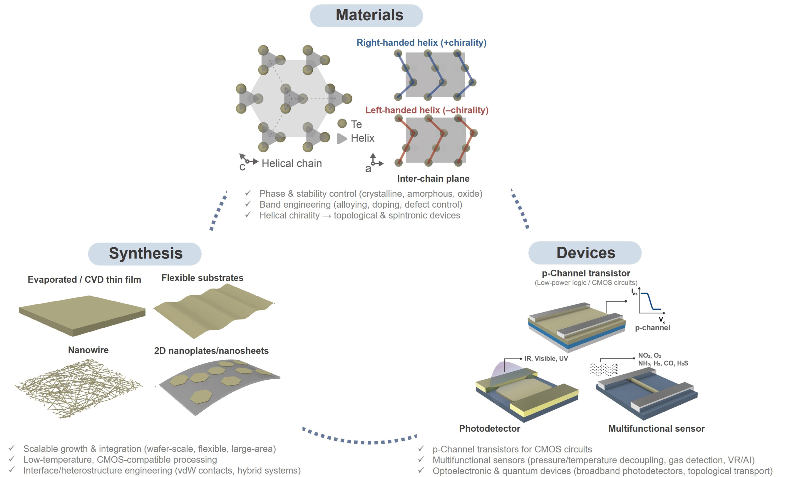
Figure 9. Outlook for Te-based electronics. Schematic summary linking materials (phase control, band engineering, chirality), synthesis (thin films, nanowires, flexible integration), and devices (p-channel transistors, photodetectors, multifunctional sensors) toward future scalable, multifunctional, and quantum applications. CVD: Chemical vapor deposition; CMOS: complementary metal-oxide semiconductor; UV: ultraviolet; VR: virtual reality; AI: artificial intelligent; IR: infrared; VdW: Van der Waals.
From a synthesis perspective, Te can be realized in diverse morphologies, including evaporated and CVD-grown thin films, nanowires, and nanoplates. Its low-temperature processability and compatibility with flexible substrates make it suitable for BEOL CMOS integration. Moreover, VdW heterostructures and hybrid systems incorporating Te provide effective routes for interface engineering, enabling improvements in charge transport, stability, and multifunctionality. Nevertheless, key challenges remain in achieving wafer-scale uniformity, reproducibility across platforms, and long-term environmental stability[34,39,45,50].
At the device level, Te-based p-channel transistors serve as an essential complement to n-type metal oxide semiconductors, enabling the realization of low-power complementary logic circuits. Te photodetectors demonstrate broadband sensitivity spanning from UV to infrared with high responsivity, while photo-thermoelectric effects enable self-powered operation. Furthermore, the coupled thermoelectric and piezoelectric properties of Te have been leveraged in multifunctional sensors capable of decoupling pressure and temperature signals or detecting specific gases. Such multifunctionality directly aligns with emerging applications in wearable electronics, virtual/augmented reality, and bio-integrated sensing systems[22,51,81].
In summary, Te and its nanostructures represent a powerful platform that bridges fundamental material physics with practical device engineering. The convergence of its unique crystallographic anisotropy, broadband tunable electronic and optical responses, and scalable synthesis technologies positions Te as a strong candidate for advanced optoelectronics, flexible electronics, and multifunctional sensing. Future research directions will need to address (i) robust phase stabilization and environmental durability, (ii) reproducible wafer-scale growth with low-temperature integration, and (iii) reliable incorporation into complex integrated circuits. Meeting these challenges will further solidify the role of Te as a versatile material at the forefront of next-generation semiconductor technologies.
In our view, many current studies on Te-based electronics still focus mainly on device performance and demonstrations. However, issues such as long-term stability, device-to-device variation, and practical integration into real circuits are often not examined in sufficient depth. We believe that Te will be most valuable not as a replacement for Si or common oxide semiconductors, but in specific areas such as broadband infrared sensing, multifunctional tactile-thermal sensors, and in-sensor computing, where its anisotropy, polymorphism, and intrinsic p-type behavior provide clear advantages. Going forward, it will be important for the field to move from proof-of-concept devices to application-driven, quantitatively benchmarked systems that show where Te-based platforms genuinely outperform existing technologies and where their limitations remain.
Challenges of tellurium-based electronics
Figure 10 summarizes the key challenges that need to be addressed for the future development of Te-based electronic devices across four major aspects. From the materials perspective, the intrinsic polymorphism of Te, including multiple crystalline and amorphous phases, poses difficulties in ensuring long-term phase stability and precise bandgap control[19,56]. Alloying strategies and oxidation engineering are therefore essential to enhance stability and enable bandgap tuning for high-performance devices[58,82]. In terms of synthesis and integration, achieving low-temperature growth compatible with conventional CMOS BEOL processes remains a prerequisite, while overcoming the heat budget limitations inherent to M3D integration is equally critical[22,83,84]. At the device level, maintaining wafer-scale uniformity of electrical properties is a persistent challenge, and sophisticated contact engineering is required to mitigate Schottky barrier formation and Fermi level pinning at metal/Te interfaces[22,85-87]. Finally, within applications and systems, large-scale integration still suffers from excessive power dissipation and inadequate thermal management, while array-level operation introduces additional complications such as reliability degradation and crosstalk between adjacent cells[47,48,58,88].
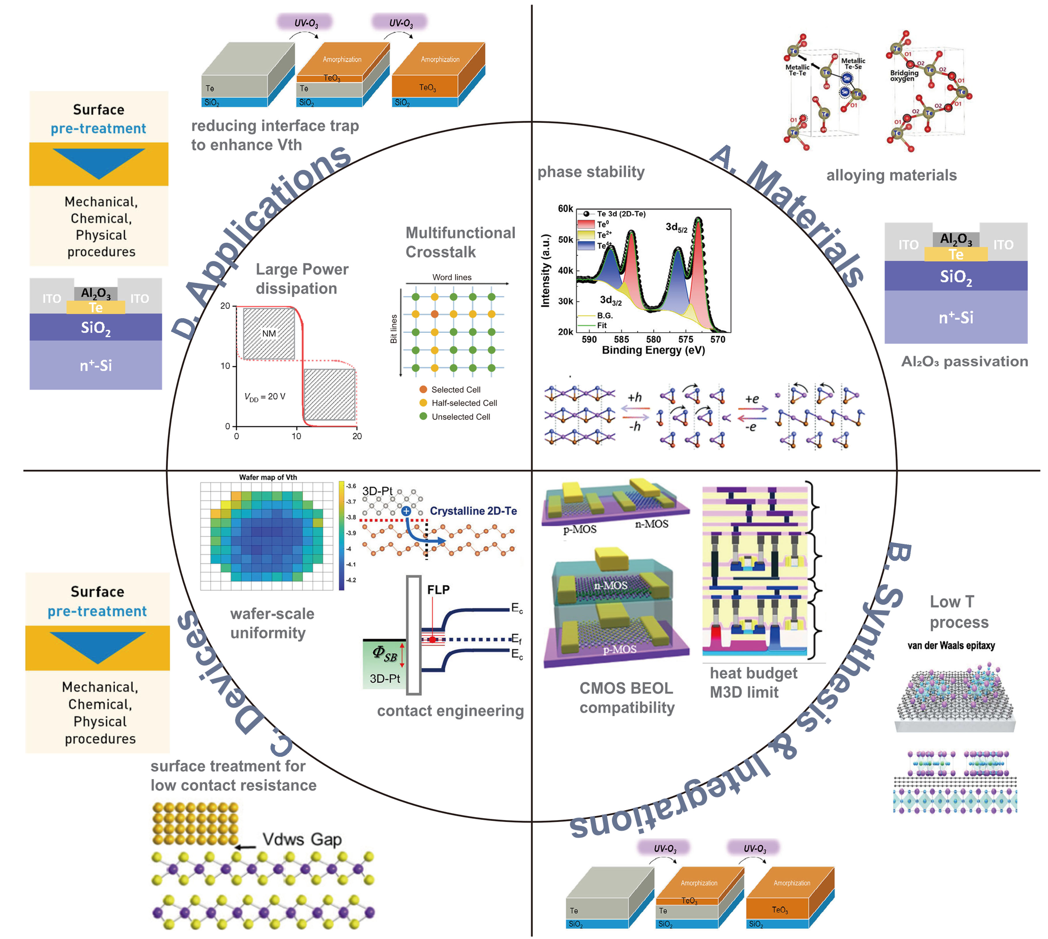
Figure 10. Challenges regarding (A) Materials: Te oxidation and phase stability; (B) Synthesis & Integration: Te-FET process compatibility with CMOS BEOL, heat limits in M3D processes; (C) Devices: wafer-scale uniformity, contact engineering to reduce contact resistance; (D) Applications: high power dissipation, multifunctional crosstalk at array scale. Figure 10A-D adapted from Refs.[19,22,56] with permission from © 2025 The Author(s). Advanced Materials, published by Wiley-VCH GmbH. FET: Field-effect transistor; CMOS: complementary metal-oxide semiconductor; BEOL: back-end-of-line; UV: ultraviolet; NM: noise margin; GND: ground; FLP: fermi level pinning; p-MOS: p-type metal oxide semiconductor.
Prioritizing these challenges suggests a staged roadmap: short-term efforts should focus on stabilizing Te phases and interfaces under realistic operating conditions; mid-term work should target scalable growth and contact engineering compatible with BEOL and M3D integration; and long-term research should address system-level issues such as thermal management, array-level crosstalk, and co-integration with digital and neuromorphic architectures.
DECLARATIONS
Author contribution
Conceived this work: Kim, J. Y.
Wrote this manuscript: Kim, J. Y.; Park, S. H.; Lee, Y. J.
Revised this manuscript: Yang, H. J.; Kim, M. W.; Kim, D. H.; Choi, S. J.
Availability of data materials
Not applicable.
Financial support and sponsorship
This work was supported by the National Research Foundation of Korea (NRF) grant, funded by the Korean government (MSIT) (RS-2025-23963262, RS-2025-16903034).
Conflicts of interest
All authors declared that there are no conflicts of interest.
Ethical approval and consent to participate
Not applicable.
Consent for publication
Not applicable.
Copyright
© The Author(s) 2026.
REFERENCES
1. Kawazoe, H.; Yanagi, H.; Ueda, K.; Hosono, H. Transparent p -type conducting oxides: design and fabrication of p-n heterojunctions. MRS. Bull. 2000, 25, 28-36.
2. Hosono, H. Ionic amorphous oxide semiconductors: material design, carrier transport, and device application. J. Non. Cryst. Solids. 2006, 352, 851-8.
3. Moon, G. D.; Ko, S.; Xia, Y.; Jeong, U. Chemical transformations in ultrathin chalcogenide nanowires. ACS. Nano. 2010, 4, 2307-19.
4. Liang, H. W.; Liu, J. W.; Qian, H. S.; Yu, S. H. Multiplex templating process in one-dimensional nanoscale: controllable synthesis, macroscopic assemblies, and applications. Acc. Chem. Res. 2013, 46, 1450-61.
5. Liu, J. W.; Zhu, J. H.; Zhang, C. L.; Liang, H. W.; Yu, S. H. Mesostructured assemblies of ultrathin superlong tellurium nanowires and their photoconductivity. J. Am. Chem. Soc. 2010, 132, 8945-52.
6. Niu, C.; Qiu, G.; Wang, Y.; et al. Tunable chirality-dependent nonlinear electrical responses in 2D tellurium. Nano. Lett. 2023, 23, 8445-53.
7. Calavalle, F.; Suárez-Rodríguez, M.; Martín-García, B.; et al. Gate-tuneable and chirality-dependent charge-to-spin conversion in tellurium nanowires. Nat. Mater. 2022, 21, 526-32.
8. Ben-Moshe, A.; da Silva, A.; Müller, A.; et al. The chain of chirality transfer in tellurium nanocrystals. Science 2021, 372, 729-33.
9. Niu, C.; Huang, S.; Ghosh, N.; et al. Tunable circular photogalvanic and photovoltaic effect in 2D tellurium with different chirality. Nano. Lett. 2023, 23, 3599-606.
11. Cao, Y.; Fatemi, V.; Fang, S.; et al. Unconventional superconductivity in magic-angle graphene superlattices. Nature 2018, 556, 43-50.
12. Novoselov, K. S.; Mishchenko, A.; Carvalho, A.; Castro Neto, A. H. 2D materials and van der Waals heterostructures. Science 2016, 353, aac9439.
13. Mayers, B.; Xia, Y. One-dimensional nanostructures of trigonal tellurium with various morphologies can be synthesized using a solution-phase approach. J. Mater. Chem. , 12, 1875-81.
14. von Hippel, A. Structure and Conductivity in the VIb group of the periodic system. J. Chem. Phys. 1948, 16, 372-80.
15. Li, Z.; Zheng, S.; Zhang, Y.; et al. Controlled synthesis of tellurium nanowires and nanotubes via a facile, efficient, and relatively green solution phase method. J. Mater. Chem. A. 2013, 1, 15046.
16. Mayers, B.; Xia, Y. Formation of tellurium nanotubes through concentration depletion at the surfaces of seeds. Adv. Mater. 2002, 14, 279-82.
17. Deckoff-jones, S.; Wang, Y.; Lin, H.; Wu, W.; Hu, J. Tellurene: a multifunctional material for midinfrared optoelectronics. ACS. Photonics. 2019, 6, 1632-8.
18. Liu, J.; Xu, J.; Hu, W.; Yang, J.; Yu, S. Systematic synthesis of tellurium nanostructures and their optical properties: from nanoparticles to nanorods, nanowires, and nanotubes. ChemNanoMat 2016, 2, 167-70.
19. Liu, A.; Kim, Y. S.; Kim, M. G.; et al. Selenium-alloyed tellurium oxide for amorphous p-channel transistors. Nature 2024, 629, 798-802.
20. Zhao, C.; Tan, C.; Lien, D. H.; et al. Evaporated tellurium thin films for p-type field-effect transistors and circuits. Nat. Nanotechnol. 2020, 15, 53-8.
21. Zhou, G.; Addou, R.; Wang, Q.; et al. High-mobility helical tellurium field-effect transistors enabled by transfer-free, low-temperature direct growth. Adv. Mater. 2018, 30, 1803109.
22. Kim, T.; Choi, C. H.; Byeon, P.; et al. Growth of high-quality semiconducting tellurium films for high-performance p-channel field-effect transistors with wafer-scale uniformity. npj. 2D. Mater. Appl. 2022, 6, 4.
23. Zhu, H.; Fan, L.; Wang, K.; Liu, H.; Zhang, J.; Yan, S. Progress in the synthesis and application of tellurium nanomaterials. Nanomaterials 2023, 13, 2057.
24. Dai, M.; Wang, C.; Qiang, B.; et al. Long-wave infrared photothermoelectric detectors with ultrahigh polarization sensitivity. Nat. Commun. 2023, 14, 3421.
25. Yao, J.; Chen, F.; Li, J.; et al. A high-performance short-wave infrared phototransistor based on a 2D tellurium/MoS2 van der Waals heterojunction. J. Mater. Chem. C. 2021, 9, 13123-31.
26. Tao, J. J.; Jiang, J.; Zhao, S. N.; et al. Fabrication of 1D Te/2D ReS2 mixed-dimensional van der Waals p-n heterojunction for high-performance phototransistor. ACS. Nano. 2021, 15, 3241-50.
27. Wang, H.; Huang, H.; Zha, J.; et al. Asymmetrically contacted tellurium short-wave infrared photodetector with low dark current and high sensitivity at room temperature. Adv. Opt. Mater. 2023, 11, 2301508.
28. Zha, J.; Xia, Y.; Shi, S.; et al. A 2D heterostructure-based multifunctional floating gate memory device for multimodal reservoir computing. Adv. Mater. 2024, 36, 2308502.
29. Bach, T. P. A.; Cho, S.; Kim, H.; Nguyen, D. A.; Im, H. 2D van der Waals heterostructure with tellurene floating-gate for wide range and multi-bit optoelectronic memory. ACS. Nano. 2024, 18, 4131-9.
30. Pokhrel, D.; Bastola, E.; Phillips, A. B.; Heben, M. J.; Ellingson, R. J. Aspect ratio controlled synthesis of tellurium nanowires for photovoltaic applications. Mater. Adv. 2020, 1, 2721-8.
31. Wu, K.; Ma, H.; Gao, Y.; Hu, W.; Yang, J. Highly-efficient heterojunction solar cells based on two-dimensional tellurene and transition metal dichalcogenides. J. Mater. Chem. A. 2019, 7, 7430-6.
32. Kolay, A.; Maity, D.; Ghosal, P.; Deepa, M. Carbon@tellurium nanostructures anchored to a Si nanowire scaffold with an unprecedented liquid-junction solar cell performance. ACS. Appl. Mater. Interfaces. 2019, 11, 47972-83.
33. Wu, L.; Huang, W.; Wang, Y.; et al. 2D tellurium based high-performance all-optical nonlinear photonic devices. Adv. Funct. Mater. 2019, 29, 1806346.
34. Liao, J.; Shao, H.; Zhang, Y.; et al. Infrared in-sensor computing based on flexible photothermoelectric tellurium nanomesh arrays. Adv. Mater. 2025, 37, 2419653.
35. Zha, J.; Shi, S.; Chaturvedi, A.; et al. Electronic/optoelectronic memory device enabled by tellurium-based 2D van der Waals heterostructure for in-sensor reservoir computing at the optical communication band. Adv. Mater. 2023, 35, 2211598.
36. Zhao, A.; Zhang, L.; Pang, Y.; Ye, C. Ordered tellurium nanowire arrays and their optical properties. Appl. Phys. A. 2005, 80, 1725-8.
37. Wang, Y.; Jin, S.; Wang, Q.; et al. Parallel nanoimprint forming of one-dimensional chiral semiconductor for strain-engineered optical properties. Nanomicro. Lett. 2020, 12, 160.
38. Wang, Y.; Wang, R.; Wan, S.; et al. Scalable nanomanufacturing and assembly of chiral-chain piezoelectric tellurium nanowires for wearable self-powered cardiovascular monitoring. Nano. Futures. 2019, 3, 011001.
39. Amani, M.; Tan, C.; Zhang, G.; et al. Solution-synthesized high-mobility tellurium nanoflakes for short-wave infrared photodetectors. ACS. Nano. 2018, 12, 7253-63.
40. Lin, S.; Li, W.; Chen, Z.; Shen, J.; Ge, B.; Pei, Y. Tellurium as a high-performance elemental thermoelectric. Nat. Commun. 2016, 7, 10287.
41. Dun, C.; Hewitt, C. A.; Huang, H.; Montgomery, D. S.; Xu, J.; Carroll, D. L. Flexible thermoelectric fabrics based on self-assembled tellurium nanorods with a large power factor. Phys. Chem. Chem. Phys. 2015, 17, 8591-5.
42. Sharma, S.; Singh, N.; Schwingenschlögl, U. Two-dimensional tellurene as excellent thermoelectric material. ACS. Appl. Energy. Mater. 2018, 1, 1950-4.
43. Peng, H.; Kioussis, N.; Snyder, G. J. Elemental tellurium as a chiral p -type thermoelectric material. Phys. Rev. B. 2014, 89, 195206.
44. Zhou, J.; Zhang, G.; Wang, W.; et al. Phase-engineered synthesis of atomically thin Te single crystals with high on-state currents. Nat. Commun. 2024, 15, 1435.
45. Jeong, U.; Rho, H. Y.; Oh, J. O.; et al. Plasma-engineered high-performance tellurium field-effect phototransistors. Adv. Funct. Mater. 2025, 35, 2421140.
46. Naqi, M.; Choi, K. H.; Yoo, H.; et al. Nanonet: low-temperature-processed tellurium nanowire network for scalable p-type field-effect transistors and a highly sensitive phototransistor array. NPG. Asia. Mater. 2021, 13, 314.
47. Huang, J.; You, C.; Wu, B.; et al. Enhanced photothermoelectric conversion in self-rolled tellurium photodetector with geometry-induced energy localization. Light. Sci. Appl. 2024, 13, 153.
48. Li, L.; Zhao, S.; Ran, W.; et al. Dual sensing signal decoupling based on tellurium anisotropy for VR interaction and neuro-reflex system application. Nat. Commun. 2022, 13, 5975.
49. Wei, X.; Wang, S.; Zhang, N.; et al. Single-orientation epitaxy of quasi-1D tellurium nanowires on M-plane sapphire for highly uniform polarization sensitive short-wave infrared photodetection. Adv. Funct. Mater. 2023, 33, 2300141.
50. Lyu, Z.; Park, M.; Tang, Y.; Choi, H.; Song, S. H.; Lee, H. J. Large-scale green method for synthesizing ultralong uniform tellurium nanowires for semiconductor devices. Nanomaterials 2024, 14, 1625.
51. Hasani, A.; Mohammadzadeh, M. R.; Ghanbari, H.; et al. Self-powered, broadband photodetector based on two-dimensional tellurium-silicon heterojunction. ACS. Omega. 2022, 7, 48383-90.
52. Spirito, D.; Marras, S.; Martín-garcía, B. Lattice dynamics in chiral tellurium by linear and circularly polarized Raman spectroscopy: crystal orientation and handedness. J. Mater. Chem. C. 2024, 12, 2544-51.
53. Dhar, N. K.; Goldsman, N.; Wood, C. E. C. Tellurium desorption kinetics from (112) Si: Si-Te binding energy. Phys. Rev. B. 2000, 61, 8256.
54. Zhou, W.; Kibler, L.; Kolb, D. Evidence for a change in valence state for tellurium adsorbed on a Pt(111) electrode. Electrochim. Acta. 2002, 47, 4501-10.
55. Lim, S.; Kim, T. I.; Park, I.; Kwon, H. Synthesis of a tellurium semiconductor with an organic-inorganic hybrid passivation layer for high-performance p-type thin film transistors. ACS. Appl. Electron. Mater. 2023, 5, 4816-25.
56. Bang, S.; Lee, C.; Choi, D.; et al. High performance p-channel transistor based on amorphous tellurium trioxide. Adv. Mater. 2025, 37, 2504948.
57. Vasileiadis, T.; Yannopoulos, S. N. Photo-induced oxidation and amorphization of trigonal tellurium: a means to engineer hybrid nanostructures and explore glass structure under spatial confinement. J. Appl. Phys. 2014, 116, 103510.
58. Zhang, Y.; Wang, J.; Xie, P.; et al. Molecular reconfiguration of disordered tellurium oxide transistors with biomimetic spectral selectivity. Adv. Mater. 2024, 36, 2412210.
59. Okuyama, K.; Kumagai, Y. Grain growth of evaporated Te films on a heated and cooled substrate. J. Appl. Phys. 1975, 46, 1473-7.
60. Dutton, R.; Muller, R. Electrical properties of tellurium thin films. Proc. IEEE. 1971, 59, 1511-7.
62. Cao, W.; Wang, L.; Xu, H. Selenium/tellurium containing polymer materials in nanobiotechnology. Nano. Today. 2015, 10, 717-36.
63. Huang, H.; Zha, J.; Xu, S.; et al. Precursor-confined chemical vapor deposition of 2D single-crystalline SexTe1-x nanosheets for p-type transistors and inverters. ACS. Nano. 2024, 18, 17293-303.
64. Kim, T.; Kim, M. J.; Lee, H.; et al. Origin of ambipolar behavior in p-type tin monoxide semiconductors: impact of oxygen vacancy defects. IEEE. Trans. Electron. Devices. 2021, 68, 4467-72.
65. Aspiala, M.; Sukhomlinov, D.; Taskinen, P. Standard Gibbs energy of formation of tellurium dioxide measurement by a solid-oxide electrolyte EMF technique. Thermochim. Acta. 2013, 573, 95-100.
66. Willey, T. M.; Bostedt, C.; van Buuren, T.; et al. Observation of quantum confinement in the occupied states of diamond clusters. Phys. Rev. B. 2006, 74, 205432.
67. Jiang, J.; Sun, L.; Gao, B.; et al. Structure dependent quantum confinement effect in hydrogen-terminated nanodiamond clusters. J. Appl. Phys. 2010, 108, 094303.
68. Hu, W.; Li, Z.; Yang, J. Surface and size effects on the charge state of NV center in nanodiamonds. Comput. Theor. Chem. 2013, 1021, 49-53.
69. Chen, Y.; Song, Z.; Liang, H.; et al. Amorphous tellurium-selenium alloy: a promising candidate material toward broadband optoelectronics. Laser. Photon. Rev. 2025, 19, e00586.
70. Qiu, G.; Huang, S.; Segovia, M.; et al. Thermoelectric performance of 2D tellurium with accumulation contacts. Nano. Lett. 2019, 19, 1955-62.
71. Xiang, Y.; Gao, S.; Xu, R.; Wu, W.; Leng, Y. Phase transition in two-dimensional tellurene under mechanical strain modulation. Nano. Energy. 2019, 58, 202-10.
72. Cai, X.; Ren, Y.; Wu, M.; Xu, D.; Luo, X. Strain-induced phase transition and giant piezoelectricity in monolayer tellurene. Nanoscale 2020, 12, 167-72.
73. Qiu, G.; Charnas, A.; Niu, C.; Wang, Y.; Wu, W.; Ye, P. D. The resurrection of tellurium as an elemental two-dimensional semiconductor. npj. 2D. Mater. Appl. 2022, 6, 17.
74. Shi, Z.; Cao, R.; Khan, K.; et al. Two-dimensional tellurium: progress, challenges, and prospects. Nano. Micro. Lett. 2020, 12, 99.
75. Zheng, T.; Yang, M.; Sun, Y.; et al. A solution-fabricated tellurium/silicon mixed-dimensional van der Waals heterojunction for self-powered photodetectors. J. Mater. Chem. C. 2022, 10, 7283-93.
76. Li, L.; Xu, H.; Li, Z.; Liu, L.; Lou, Z.; Wang, L. CMOS-compatible tellurium/silicon ultra-fast near-infrared photodetector. Small 2023, 19, 2303114.
77. Li, L.; Zhang, G.; Younis, M.; et al. 2D tellurium films based self-drive near infrared photodetector. Chemphyschem 2024, 25, e202400383.
78. Choi, T. Y.; Kang, J. H.; Jang, J. H.; Kim, H. K. High-performance flexible 2D tellurium semiconductor grown by isolated plasma soft deposition for wearable and flexible temperature sensors. Small. Methods. 2025, 9, 2500379.
79. Rani, A.; Sultan, M. J.; Ren, W.; et al. Bio-inspired photosensory artificial synapse based on functionalized tellurium multiropes for neuromorphic computing. Small 2024, 20, 2310013.
80. Wang, Y.; Qiu, G.; Wang, R.; et al. Field-effect transistors made from solution-grown two-dimensional tellurene. Nat. Electron. 2018, 1, 228-36.
81. Choi, I. J.; Kim, B. J.; Lee, S. H.; et al. Fabrication of a room-temperature NO2 gas sensor using morphology controlled CVD-grown tellurium nanostructures. Sens. Actuators. B. Chem. 2021, 333, 128891.
82. Meng, Y.; Wang, W.; Fan, R.; et al. An inorganic-blended p-type semiconductor with robust electrical and mechanical properties. Nat. Commun. 2024, 15, 4440.
83. Niu, C.; Tan, P.; Lin, J. Y.; et al. First demonstration of BEOL wafer-scale all-ALD channel CFETs using IGZO and Te for monolithic 3D integration. In 2024 IEEE International Electron Devices Meeting (IEDM), San Francisco, CA, USA, December, 07-11, 2024; IEEE, 2024, pp. 1-4.
84. Kim, M.; Lee, Y.; Kim, K.; et al. Processes to enable hysteresis-free operation of ultrathin ALD Te p-channel field-effect transistors. Nanoscale. Horiz. 2024, 9, 1990-8.
85. Hu, J.; Wang, B.; Li, X.; et al. Oxygen plasma induced improvement of contact resistance and mobility of tellurium field-effect transistor. Appl. Phys. Lett. 2025, 126, 193101.
86. Jiang, W.; Wang, X.; Chen, Y.; et al. End-bonded contacts of tellurium transistors. ACS. Appl. Mater. Interfaces. 2021, 13, 7766-72.
87. Lin, Z.; Wang, J.; Chen, J.; et al. Two-dimensional tellurene transistors with low contact resistance and self-aligned catalytic thinning process. Adv. Elect. Mater. 2022, 8, 2200380.
Cite This Article
How to Cite
Download Citation
Export Citation File:
Type of Import
Tips on Downloading Citation
Citation Manager File Format
Type of Import
Direct Import: When the Direct Import option is selected (the default state), a dialogue box will give you the option to Save or Open the downloaded citation data. Choosing Open will either launch your citation manager or give you a choice of applications with which to use the metadata. The Save option saves the file locally for later use.
Indirect Import: When the Indirect Import option is selected, the metadata is displayed and may be copied and pasted as needed.
About This Article
Special Topic
Copyright

Data & Comments
Data
0


Comments
Comments must be written in English. Spam, offensive content, impersonation, and private information will not be permitted. If any comment is reported and identified as inappropriate content by OAE staff, the comment will be removed without notice. If you have any queries or need any help, please contact us at [email protected].