


fig6
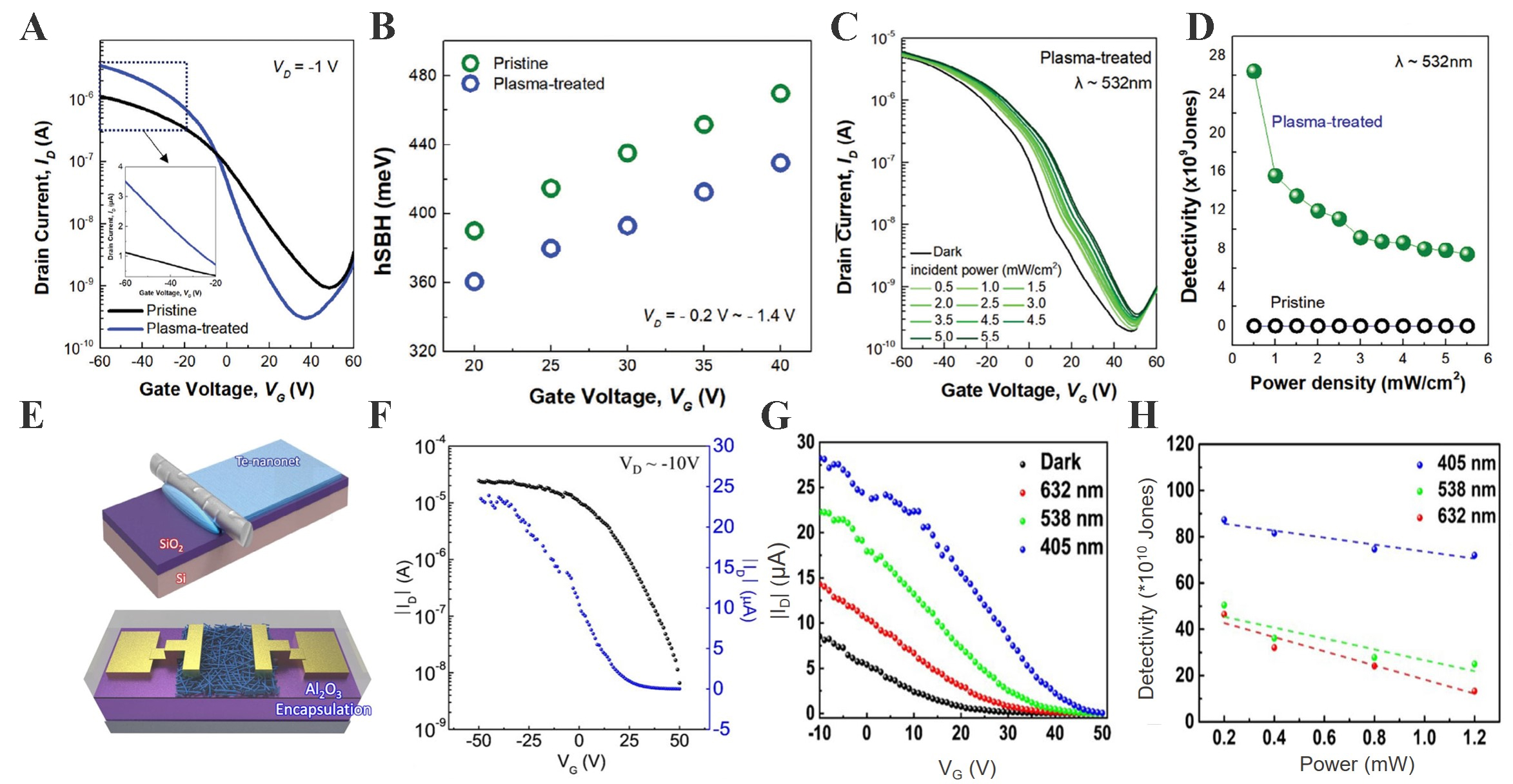
Figure 6. Electrical and optoelectronic properties of plasma-treated TeFETs and Te-nanonetwork transistors. (A) Transfer curves of pristine vs. plasma-treated TeFETs, showing enhanced on-current and suppressed off-current; (B) Extracted hole Schottky barrier height, reduced after plasma treatment; (C) Transfer characteristics under 532 nm illumination with varying power densities, highlighting increased photocurrent; (D) Detectivity as a function of optical power, demonstrating superior photodetection in plasma-treated devices[45]; (A-D) Adapted from Ref.[45] with permission from Wiley-VCH Verlag GmbH & Co. KGaA. (E) Schematic of Te-nanonetwork transistor with Al2O3 encapsulation; (F) Transfer curves in the dark, showing stable p-type behavior with high on/off ratio; (G) Wavelength-dependent photoresponse under 405, 538, and 632 nm illumination; (H) Detectivity versus optical power at different wavelengths, confirming wavelength-sensitive photodetection[46]. (E-H) Adapted from Ref.[46] under the Creative Commons CC BY license. FET: Field-effect transistor.


