


fig7
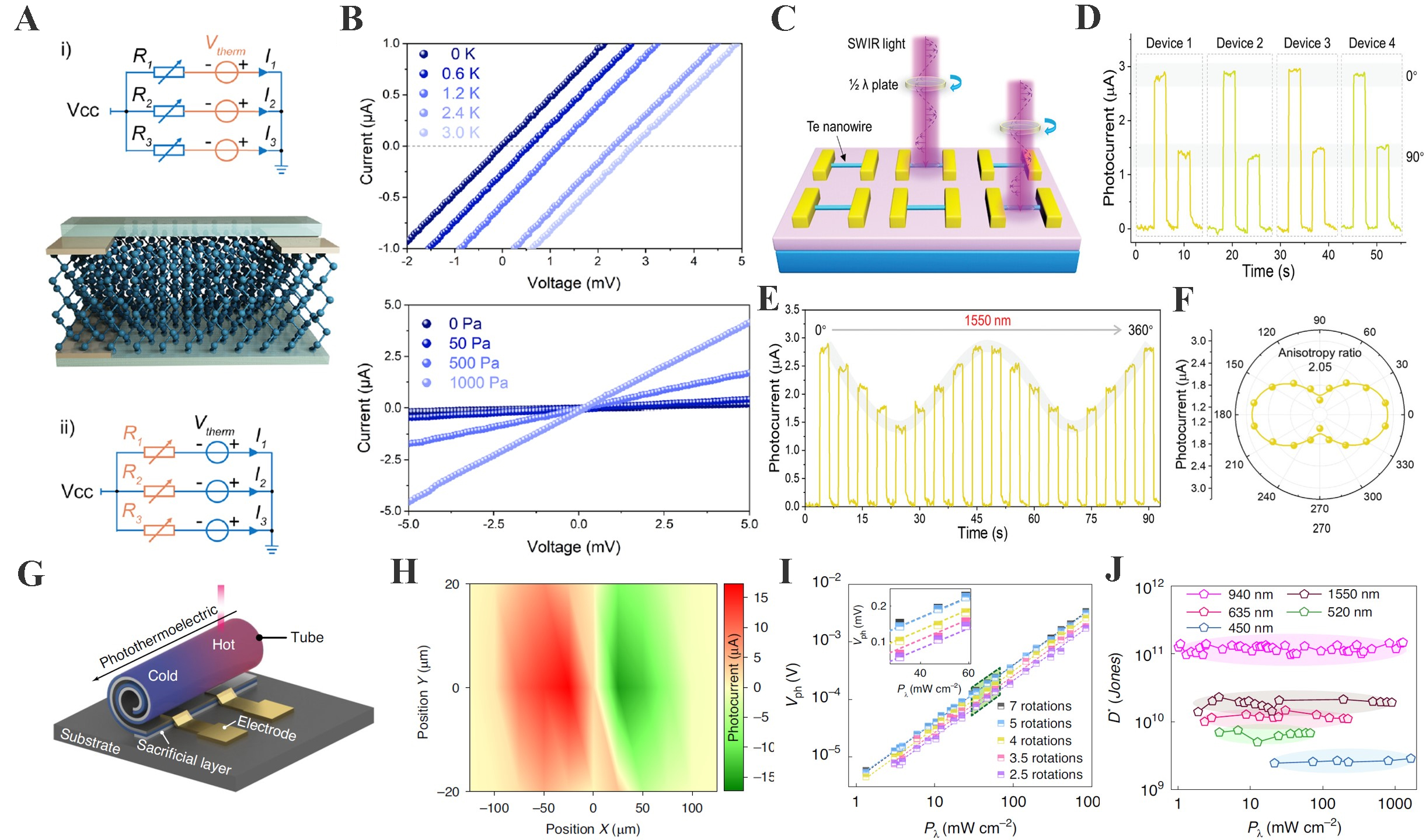
Figure 7. Multifunctional Te-based sensors and photodetectors. (A) Working principle and equivalent circuits of Te nanowire-based bimodal tactile sensors under thermal and pressure stimuli; (B) I-V curves showing thermoelectric response at low temperatures (top) and piezoresistive behavior under applied pressures (bottom)[48]; (A and B) Adapted from Ref.[48] under the Creative Commons CC BY license. (C) Polarization-dependent SWIR measurement setup using a half-wave plate and aligned Te nanowires; (D) Photocurrent of four devices under 1,550 nm illumination at 0°/90° polarization; (E) Time-resolved response during continuous polarization rotation (0-360°); (F) Polar plot confirming anisotropic photocurrent behavior[49]; (C and D) Adapted from Ref.[49] with permission from Wiley-VCH Verlag GmbH & Co. KGaA. (G) Schematic of a self-rolled Te tubular photothermoelectric detector; (H) Spatial photocurrent mapping at 940 nm, showing geometry-dependent response; (I) Photovoltage versus incident power for different rolling rotations, exhibiting linear scaling; (J) Detectivity across multiple wavelengths (450-1,550 nm), demonstrating broadband high-sensitivity performance[47]. Adapted from Ref.[47] under the Creative Commons CC BY license. I-V: Current-voltage; SWIR: short-wave infrared.


