


fig4
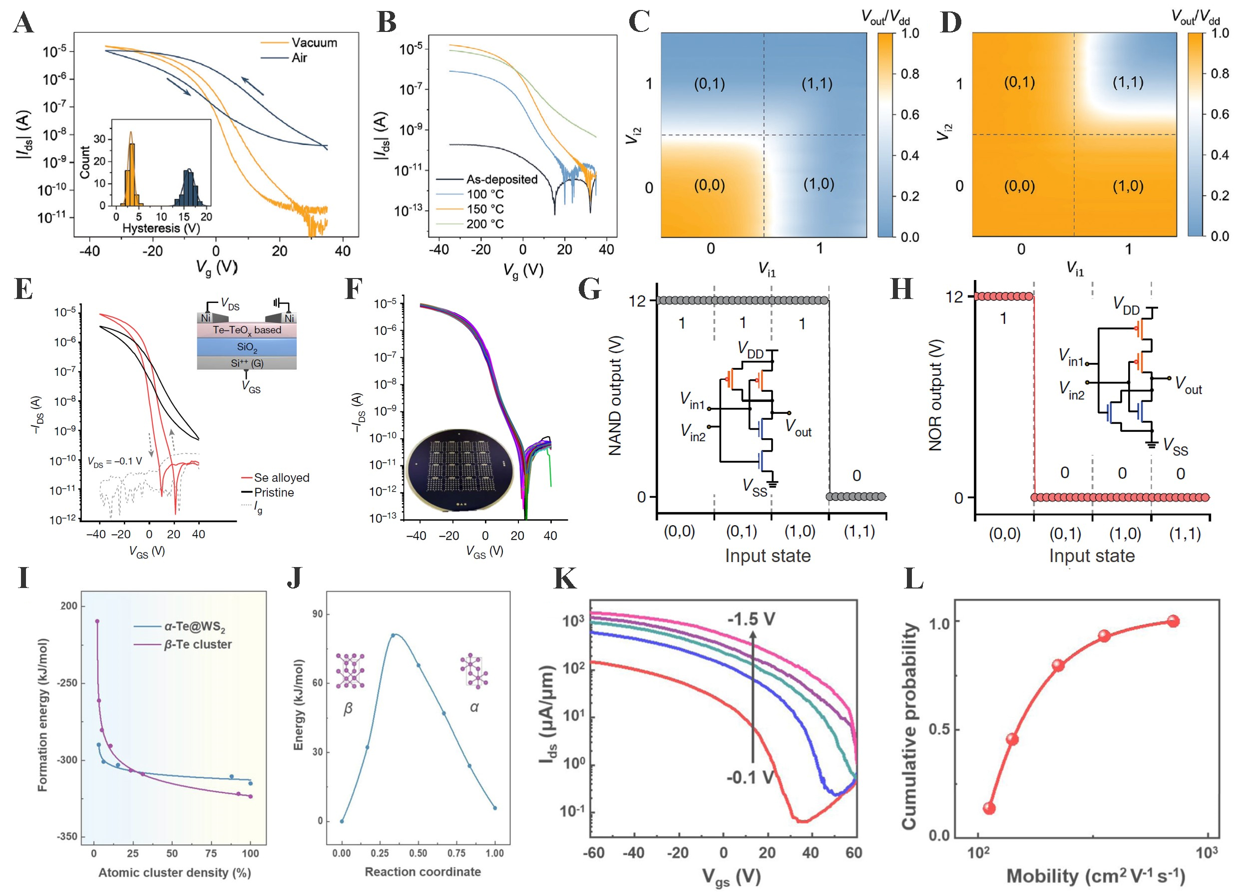
Figure 4. Device stability, logic operation, phase engineering, and transport characteristics in Te-based transistors. (A) Transfer curves of FETs measured in vacuum and air, showing mode change driven by oxygen adsorption; (B) Transfer characteristics after thermal annealing at different temperatures, indicating improved switching behavior; (C) NAND logic output map demonstrating correct low-output at (1,1); (D) NOR logic output map showing high output only at (0,0)[58]; (A-D) Adapted from Ref.[58] with permission from Wiley-VCH Verlag GmbH & Co. KGaA. (E) Transfer curves of pristine and Se-alloyed Te-TeOx TFTs, showing reduced onset voltage and suppressed leakage; (F) Transfer curves of 80 Se-alloyed Te-TeOx TFTs, highlighting wafer-scale uniformity; (G) Output characteristics of a complementary NAND gate combining p-channel Te-TeOx and n-channel In2O3 TFTs; (H) NOR gate characteristics from the same complementary TFTs, showing correct logic operation[19]; (E-H) Adapted from Ref.[19] under the Creative Commons CC-BY license. (I) Formation energy of α- and β-Te as a function of atomic cluster density on WS2, indicating α-phase favored at low density and β-phase at high density; (J) Calculated transition barrier between α- and β-phases; (K) Transfer curves of β-Te FETs under various drain biases; (L) Cumulative mobility distribution of β-Te devices[44]. (I-L) Adapted from Ref.[44] under the Creative Commons CC BY license. FET: Field-effect transistor; NAND: NOT AND; TFT: thin film transistor.


