


fig5
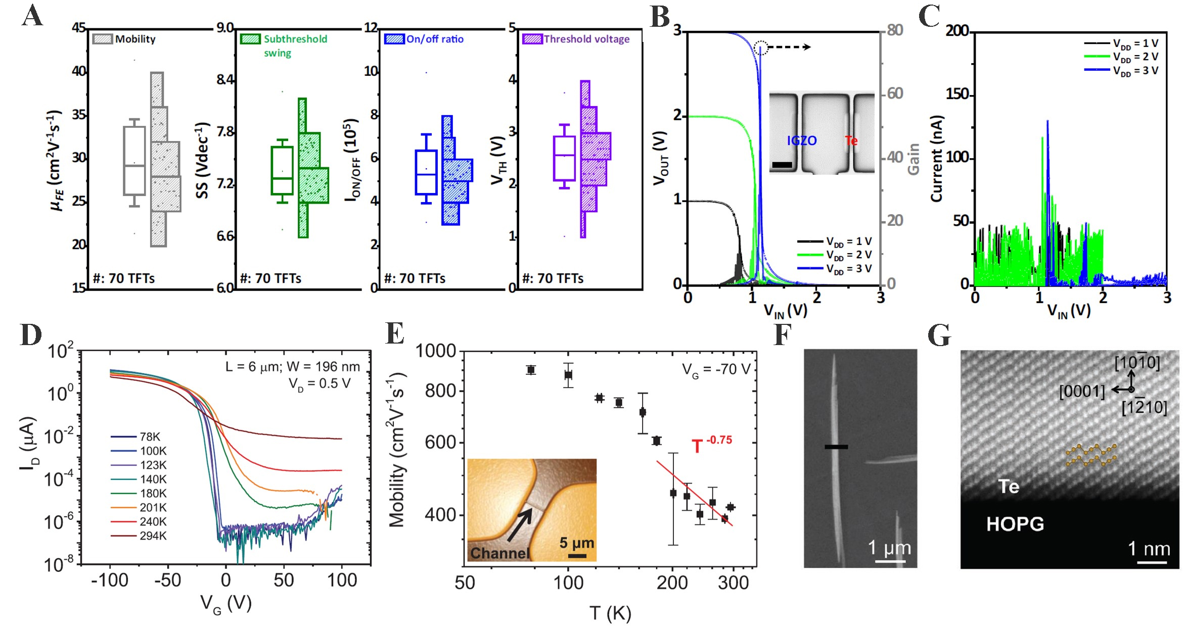
Figure 5. Device statistics, CMOS inverter operation, and temperature-dependent transport in Te-based transistors. (A) Statistical distribution of field-effect mobility (µFE), subthreshold swing (SS), on/off ratio (ION/IOFF), and threshold voltage (Vth) extracted from 70 Te-based transistors; (B) Voltage transfer curves and corresponding gain of a CMOS inverter composed of IGZO n-channel and Te p-channel transistors at VDD = 1-3 V (inset: optical micrograph, scale bar, 2 µm); (C) Static current characteristics of the CMOS inverter under different VDD values[22]; (A-C) Adapted from Ref.[22] under the Creative Commons CC BY license. (D) Transfer curves (Ids - Vgs) of Te-based transistors measured from 78 K to 294 K (L = 6 µm, W = 196 nm, VD = 0.5 V); (E) Temperature-dependent mobility following a phonon-limited T-0.75 relation (inset: optical image of the transistor channel, scale bar, 5 µm); (F) SEM image of needle-like Te nanostructures grown on HOPG (scale bar, 1 µm); (G) Atomically resolved STEM image of the Te/HOPG interface along [0001], revealing the helical chain structure (scale bar, 1 nm)[21]; (D-G) Adapted from Ref.[21] with permission from Wiley-VCH Verlag GmbH & Co. KGaA. CMOS: Complementary metal-oxide semiconductor; IGZO: indium gallium zinc oxide; HOPG: highly oriented pyrolytic graphite; STEM: scanning transmission electron microscopy; SEM: scanning electron microscope.


