


fig1
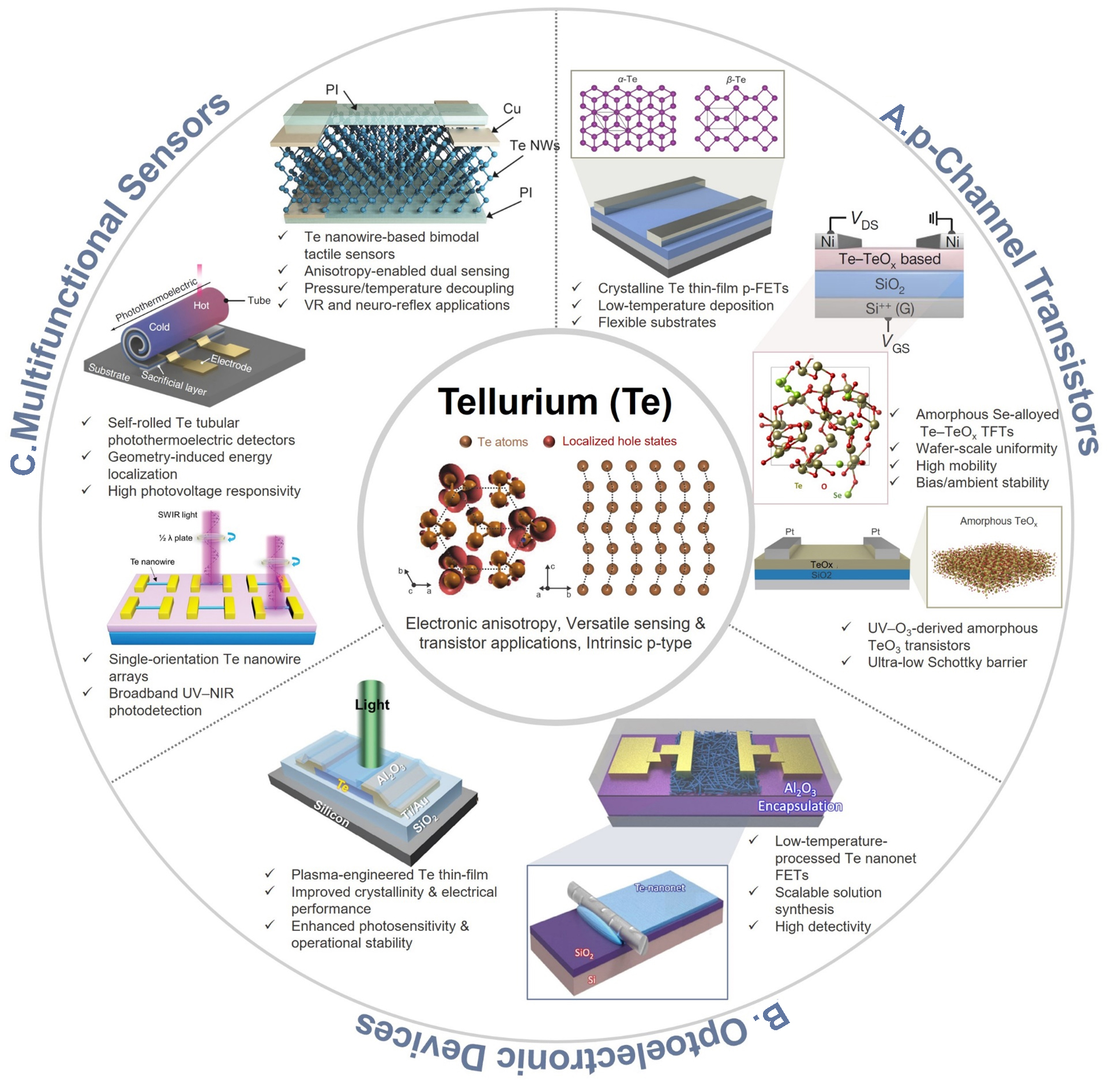
Figure 1. Te-based device applications. The central panel illustrates the crystal structure of Te. Adapted from Ref.[18] with permission from Copyright by Wiley-VCH Verlag GmbH & Co. KGaA. (A) p-Channel Transistors: Crystalline and amorphous Te-based FETs with high mobility, scalability, and ultra-low contact barriers[19,44]. Adapted from Ref.[19] and Ref.[44] under the Creative Commons CC BY license(s). (B) Optoelectronic Devices: Plasma-engineered and nanonetwork Te transistors offering enhanced photosensitivity, stability, and scalable fabrication[45,46]. Adapted from Ref.[45] with permission from Wiley-VCH Verlag GmbH & Co. KGaA; and from Ref.[46] under the Creative Commons CC BY license. (C) Multifunctional Sensors: Te nanowire, tubular, and heterojunction devices enabling dual sensing, photothermoelectric detection, and broadband UV-NIR photodetection[47-49]. Adapted from Ref.[49] with permission from Wiley-VCH Verlag GmbH & Co. KGaA; and from Refs.[47,48] under the Creative Commons CC BY license. UV-NIR: Ultraviolet- near-infrared; FET: field-effect transistor; PI: polyimide; p-FETs: p-channel FETs; NMs: nanomeshs.


