


fig8
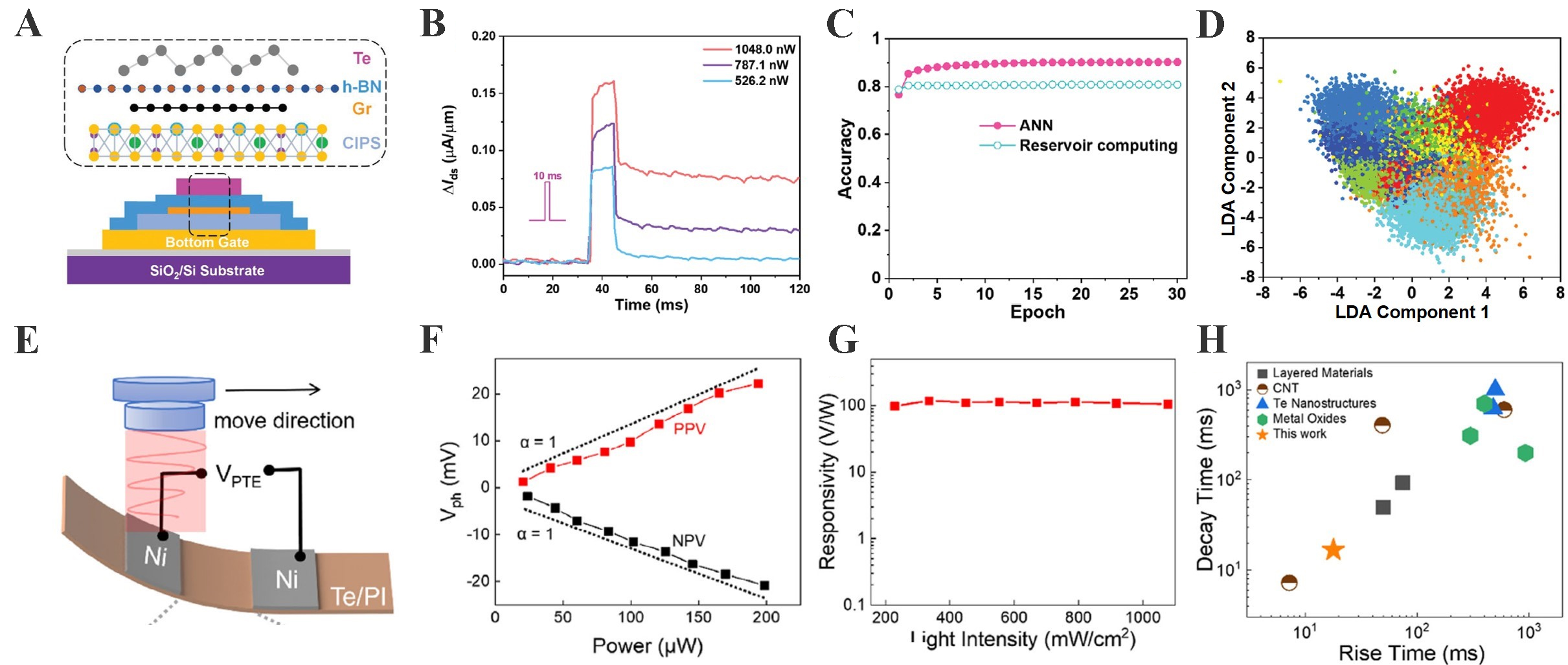
Figure 8. In-sensor memory and photothermoelectric performance of Te-based devices. (A) Schematic of the Te/h-BN/graphene/CIPS van der Waals heterostructure memory device on SiO2/Si; (B) Channel conductance modulation (ΔIds) under 1,550-nm optical pulses at different powers, showing short-term potentiation; (C) Recognition accuracy for handwritten digits using ANN and reservoir computing frameworks; (D) LDA plots of reservoir outputs, illustrating well-clustered feature distributions[35]; (A-D) Adapted from Ref.[35] with permission from Copyright by Wiley-VCH Verlag GmbH & Co. KGaA. (E) Schematic of the flexible Te nanomesh photothermoelectric detector, where laser illumination induces position-dependent V_PTE; (F) Photovoltage response versus incident power, exhibiting near-linear dependence (α ≈ 1) for PPV and NPV modes; (G) Responsivity under 1,550-nm excitation across varying light intensities, remaining ~120 V W-1; (H) Rise and decay times of Te nanomesh detectors compared with other photodetectors, highlighting competitive response speed[34]; (E-H) Adapted from Ref.[34] with permission from Wiley-VCH Verlag GmbH & Co. KGaA. CIPS: CulnP2S6; ANN: artificial neural network; LDA: linear discriminative analysis; PPV: positive photovoltage; NPV: negative photovoltage; h-BN: hexagonal-Boron Nitride; V_PTE: photothermoelectric voltage; CNT: carbon nano tube.


