


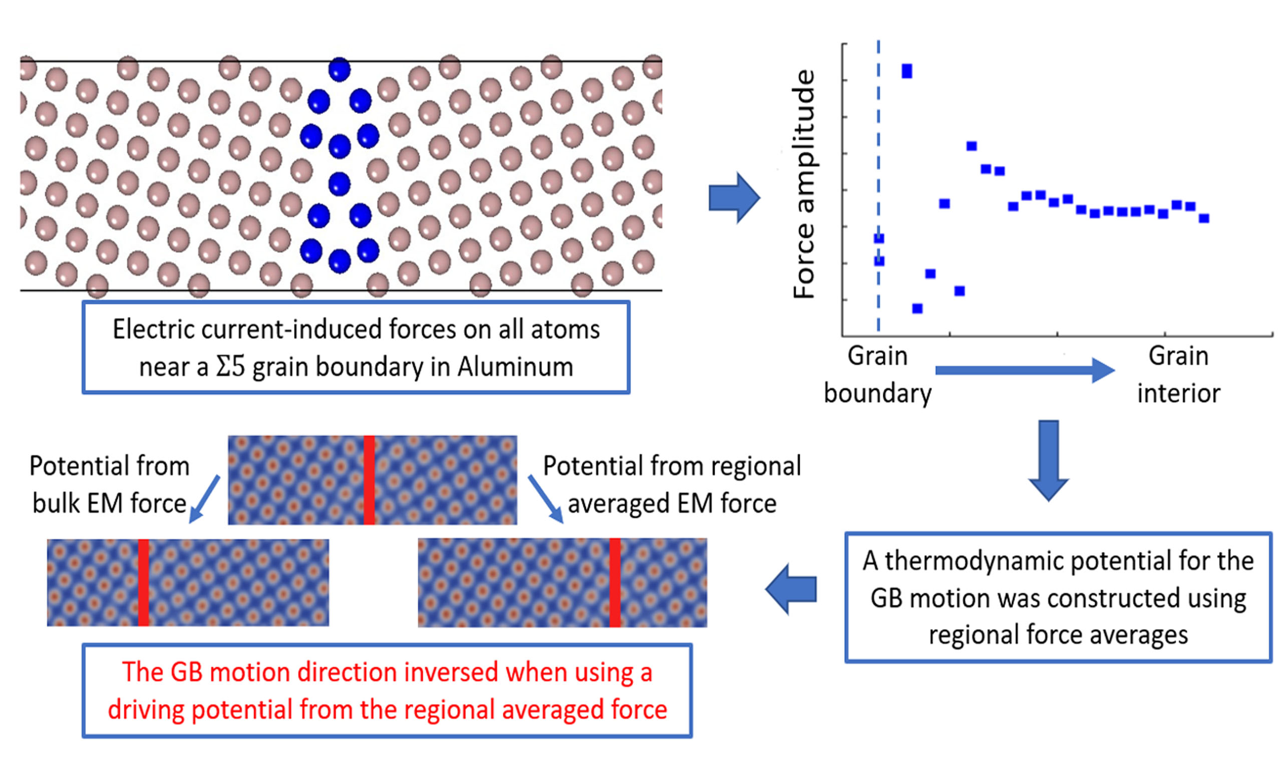
Determination of electric current induced motion of a symmetrically tilt Σ5 grain boundary in aluminum using quantum transport calculations
 0
0 
Abstract
Electric current induced structural change is a critical reliability issue in nanoelectronics. So far, microstructure evolution models have considered the electromigration (EM) force caused by high current density to be uniform everywhere in the conductor. In this work, the EM force acting on atoms near Σ5 grain boundaries (GBs) of aluminum is calculated for the first time using a quantum transport method. Although the EM forces exhibit a complex distribution near the GB, the regional averaged EM force from GB atoms points toward the opposite direction of the bulk EM force. This striking result leads to GB motion in the direction of the electron current, whereas previous structural evolution models considering uniform EM forces predict GB motion in the opposite direction. This result highlights the necessity to consider the current-induced grain structure evolution at quantum mechanical level since the local EM force on atoms depends on the electron scattering behavior of the GB structure.
Keywords
INTRODUCTION
It has long been known that high density electric current leads to microstructure change in metals. Other than the Joule heating effect, electromigration (EM) of atoms due to scattering and momentum transfer of conduction electrons is the key mechanism for the structural evolution[1]. The EM forces in bulk crystals have been quantified through experiments and quantum mechanical calculations[2-4]. Many EM related experimental and theoretical studies focused on interconnects failure in integrated circuits (ICs), since it has a strong impact on the service life of IC chips[5,6]. EM is also important in the functioning of several emerging nanoelectronics devices. In metallurgy, high density electric pulses have been used for tuning microstructures for a long time, and the current-induced structural change was known as electro-plastic effect[7]. Current-induced phenomena related to important microstructural defects like grain boundaries (GBs) and second-phase precipitates have been reported in experiments[8-10], but comprehensive theoretical and computational studies on current-induced evolution of these important microstructural features are still largely missing.
The EM process have been explained phenomenologically using a classical biased diffusion equation, which contains an additional term representing the driving force caused by the EM force on atoms, expressed as an effective EM charge[5]. The origin of the EM force has also been discussed based on scattering of conduction electrons using quantum mechanical theories[11]. The experimentally measured effective EM charges have been reproduced in quantum mechanical calculations by evaluating the force on the atom next to a vacancy in single crystals[8,9].
Previous computational studies dealing with EM induced microstructure evolution also incorporated the EM force phenomenologically using the effective EM charge[12-15]. It is a common knowledge that materials microstructure has a strong effect on its electric conductivity due to different mechanisms of electron scattering from GBs and precipitates[16], but when it comes to the EM force, which is also originated from the electron scattering, only the bulk single crystal version of the EM force was used in modelling current-induced microstructure evolution. A structural evolution model considering the details of electron scattering and the associated forces on atoms near GBs and precipitates is mostly missing.
Previous calculations using the quantum transport theory[17,18] have shown that the EM force on surface step atoms is much larger than the force on bulk lattice atoms since they scatter conduction electrons differently. Similarly, deviation of the EM force on atoms near a GB or precipitate from its bulk value is expected, as well. However, to the best of our knowledge, no quantum mechanical calculations have been carried out to extract the EM force on atoms near a GB or precipitate.
In the timescales of microstructure evolution, the GB migration follows a coarse-grained description where the motions of individual atoms near the GB are coarse-grained into an averaged behavior of the GB motion with its velocity given by v = mp where m is the GB mobility, and p is the thermodynamic driving force. Although the EM force near the GB is expected to be rather complicated due to variations in the GB atomic structures and the associated kinetic processes during the GB migration[19], a coarse-grained EM force over atoms near the GB, from which a thermodynamic driving force for GB migration can be constructed, is still very useful in mesoscale modelling studies of current-induced microstructure evolution[20,21].
In this study we carry out calculations of the EM forces on atoms near a symmetrical tilt Σ5 GB in Al (F.C.C.) crystal, and attempted to extract coarse-grained features of the EM force for microstructure evolution models. To our knowledge, this is the first work trying to resolve the EM forces near a complex GB and link the average EM force to electric current induced microstructural change in metals. The paper is organized as follows. Section 2.1 presents the theory outlining the calculations of the EM force in a quantum transport system, and Section 2.2 describes other methods used to construct the GB. Section 2.3 introduces an electric-current driven microstructure evolution model for testing the coarse-grained EM force. Then, the resulting EM forces on atoms near the GB are presented in Section 3.1, followed by an analysis for extracting coarse-grained features from the forces in Section 3.2. The GB motion is demonstrated based on the coarse-grained force using the structural evolution model in Section 3.3, followed by concluding remarks in Section 4.
THEORY AND METHODS
Evaluating the EM force from quantum transport calculations
The quantum transport method for calculating the EM force is briefly introduced here. An electron transport system can be represented by three parts, including two contacts at the edges and a conductor channel connecting between them. The two contacts serve as source and drain, where electrons are transported from the source to the drain through the channel. Quantum transport theories[22] have shown that electrons in the conductor channel can be well described by two wavefunctions, ϕL from the left (source) and ϕR from the right (drain). The current in the transport region is given by
where the summation over k is for momentum and over s is for spin; je is the current operator; and fL,R (E) is the biased Fermi distribution function. It differs from the equilibrium Fermi function being controlled by the electrochemical potential μL,R in the left/right contact originating from electric voltage. Similarly, the force on the ith atom at position Ri is given by
where
where the two forces on the right are calculated under the biased and equilibrium conditions.
Combining the equations 2 and 3, one can see that the EM force is the difference of the Feynman-Hellmann force
The electron wavefunctions and the forces on atoms are calculated using the Nanodcal software applying the non-equilibrium Green’s function (NEGF) method[23]. It has been shown in previous works[24,25] that the NEGF based Landauer formulation used in our work captures the GB reflection behavior in transport quite well. Since both the reflection and EM force are results from the scattering of conduction electrons, this method is expected to provide reasonable results for EM forces on GB atoms.
Construction of the slab model comprising a GB
The transport system comprising a symmetric tilt Σ5 GB is shown in Figure 1. It was constructed as follows.
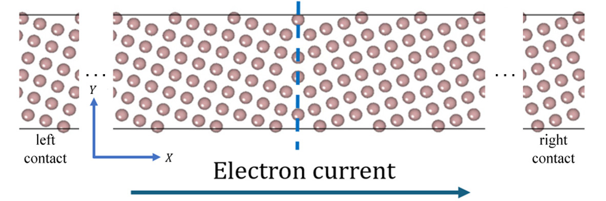
Figure 1. A bi-crystal system for electron transport calculation. The Σ5 tilt grain boundary (GB) is marked by the dashed line. The left and right contacts are also shown. The figure was prepared using Matlab.
Two face centered cubic (FCC)-Al single crystals were firstly constructed separately with the three principal axes aligned along the X, Y, and Z coordinates of the simulation box. Since the misorientation angle of the Σ5 GB is θ = 36.9°, one crystal was rotated an angle θ/2 clockwise along the Z axis (perpendicular to the view in Figure 1), while the other crystal was rotated θ/2 counterclockwise; the two crystals were then joint together along the X direction to form a bi-crystal structure. All the atom manipulations were performed using the Atomsk software[26]. The bi-crystal structure was then simulated using the molecular dynamics (MD) package LAMMPS[27] for structural relaxation applying the embedded atom model (EAM) interatomic potential[28] in the constant particle number, volume and temperature (NVT) ensemble with conjugate gradient algorithm. The system size along the Z direction is equal to the lattice constant a0 of Al, the system size along the Y direction is carefully chosen to be
The bi-crystal structure obtained from the MD procedure above is then imported into the density functional theory (DFT) software DS-PAW, which implements the Projector Augmented Wave potential[29], for further structural relaxation prior to the transport calculations described at the beginning of this section.
In the transport calculation, only the GB at the center of the simulation domain was kept, while the other GB at the end of the simulation domain produced by the periodic boundary is cut out by truncating the simulation domain in the previous step. It is important to note that, although the full transport system is not periodic, the left and right contact regions selected in the transport calculation should be periodic in order to obtain the correct wavefunctions in the contact region.
Current-driven microstructure evolution model
Several models based on phase-field (PF) type[30,31] methods have been proposed for studying electric current induced structural evolution. The EM forces in these models are incorporated through an energy density term based on the bulk effective EM charge in the free energy functional[14,15,32]. Here, a previously formulated phase-field-crystal (PFC) model is briefly reviewed, and will further on serve as the testing model for the coarse-grained EM force on GB atoms. This is due to the relation between the classical diffusion-based EM theory and the quantum mechanical EM force that is established in this method[33].
The PFC model starts with an energy functional given by:
where
Evolution of the microstructure is captured in this model by tracking the change of the local density parameter using variation principle
Numerical simulations of the current induced GB motion are carried out in a slab bi-crystal geometry constructed using the same method explained in section 2.2. The density evolution equation
RESULTS AND DISCUSSION
EM forces on atoms near the GB
Before calculating the EM force on atoms near the GB, a method validation was carried out first. The EM force on bulk atoms was checked using the simple LDA functional[34] which was also used in previous studies[17], and the result is shown in the Supplementary Materials. K-point sampling of (5, 2, 15), energy cutoff of 1,000 eV, and the convergence criteria of 10-4 Hartree are used in the Nanodcal calculations. The applied potential biases between the two contacts are carefully chosen such that the resulting electric current density is on the order of 106 - 107 A/cm2 which is the typical current density for the EM.
The EM forces on atoms near the Al Σ5 GB is shown in Figure 2.
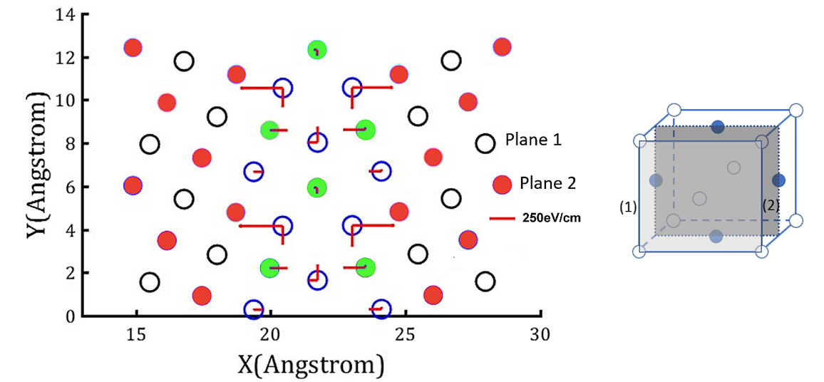
Figure 2. The calculated EM forces acting on GB atoms along the two in-plane directions are shown in the left panel. The applied electric field is 6.8 V/cm. The force amplitude is marked by the length of the arrows with a scale bar shown in the figure. The hollow dots are atoms in plane 1, the solid dots are atoms in plane 2. The plane 1 and 2 are illustrated in the FCC structure shown in the right panel as the light grey and dark grey planes respectively. The orange colored solid dots and blue colored hollow dots on the left panel are marked as GB atoms. The figure was prepared using Matlab. EM: Electromigration; GB: grain boundary; FCC: face centered cubic.
Since atoms jump across the GB during the GB motion, the forces along the jumping direction, which coincides with the electron transport direction in this study, are plotted in Figure 3. The forces perpendicular to the electron transport direction is not relevant to the atom jump across the GB and are ignored in further analysis.
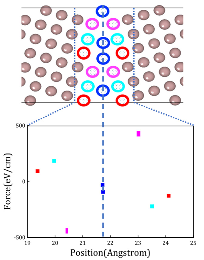
Figure 3. The EM force on GB atoms along the electron current direction are shown at the bottom panel under the applied electric field of 6.8 V/cm. The GB atom configuration is shown in the top panel. The center dash line marks the GB position in the two panels. The dotted lines in the top panel marks the region for the force plot shown in the bottom panel. The center dark blue data points in the bottom panel are the forces on the dark blue atoms shown in the GB region in the top panel. Data points are mostly overlapped since there are two identical structural units along the GB plane. The pink, cyan and red data points correspond to the same colored atoms at the top panel. The figure was prepared using Matlab. EM: Electromigration; GB: grain boundary.
These forces seem to have an anti-symmetric feature with respect to the GB plane and change significantly from atom to atom. It is not surprising that the EM forces on GB atoms are very complex considering the disordered atomic structure at the GB. Since our purpose is to find an effective potential from which the EM force on atoms can be recovered in the microstructure evolution model, the large variations of the EM force on the near GB atoms has to be treated carefully. Instead of trying to incorporate these detailed forces, which depend strongly on the atom positions and will change drastically during the GB motion, into a model of GB migration, they should be averaged in a thermodynamic sense. The averaged force leads to a thermodynamic potential for atoms in the corresponding region which serves as the driving force for the GB motion in MD and mesoscale models[21,35]. Also, due to the small amplitude of these forces, one would not expect a significant distortion of the GB structure.
In order to identify averaged features in these EM forces, an extended force plot is shown in Figure 4 including atoms far away from the GB.
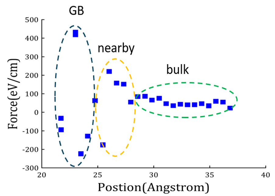
Figure 4. EM forces on atoms in the right half of the bi-crystal structure along the electron transport direction. The applied electric field is 6.8 V/cm. The three dashed circles marked the forces from different regions. The GB center is located at the two left-most data points since there are two atoms at the GB within one structural unit as shown in Figure 3. The figure was prepared using Gnuplot. EM: Electromigration; GB: grain boundary.
One can clearly identify 3 regions in Figure 4, a GB region, a near GB region (marked as nearby), and a bulk region. In the GB region, the forces change drastically from atom to atom, whereas in the near GB region the forces still change but not as drastically as in the GB region. Finally, in the bulk region, the forces are nearly equal to each other with slight fluctuations about an average value of 50 eV/cm. The thickness of the GB region and the near GB region together is about 0.7 nm. This is an expected feature due to strong scattering of conduction electrons near the GB. The Fermi energy of conduction electrons in Al is 11.6 eV and the corresponding de Broglie wavelength is 0.36 nm. Atoms far away from the GB (in a distance significantly larger than the electron wavelength) are expected to exhibit the bulk behavior, as shown in the bulk region in Figure 4. While the EM force results shown in Figures 2 and 3 may seem small comparing with the typical force from a chemical bond, this is exactly why the EM effect will only manifest itself in the diffusion timescales as described in the classic Blech effect[5]. For a typical metal system with the lattice diffusion barrier about 0.1 eV[36], the EM force will only add a small tilt to the diffusion barrier which leads to preferred atom diffusion along the force direction. To the best of our knowledge, this work is by far the first study of the electromigration force near a grain boundary which is a very important microstructure defect.
Coarse-grained EM force near GBs
With insights gained from Figure 4, the regional force averages are calculated using a simple arithmetic mean of forces on the atoms in the GB, near GBs, and bulk regions under various external voltage bias, and the results are shown in Figure 5. Please note that the forces in figure 4 are along the electron transport direction while the forces in Figure 5 is along the electric current direction. Both sides of the bi-crystal are taken into account in calculating the average forces.
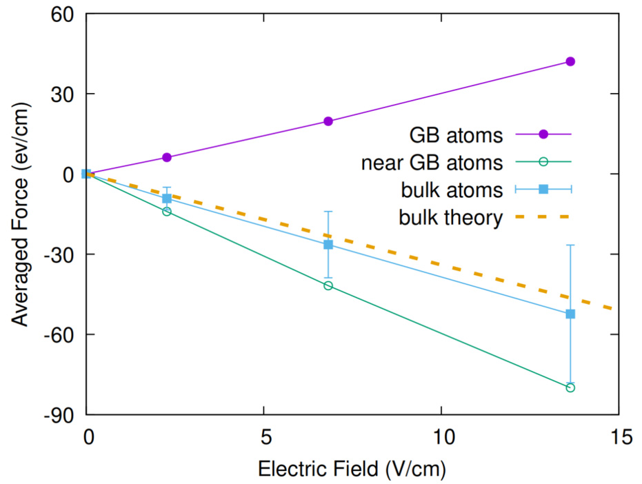
Figure 5. Regional-averaged force along the electric current direction under different electric fields. Data points are shown in dots and connected using solid lines. The dashed theory line is calculated using an effective EM charge Z* = -3.4 based on ref.[4]. The error bar for the averaged force on bulk atoms indicates the fluctuation range of the EM force in the bulk. No error on the average forces from the GB and near GB regions is considered since the average there are used to extract region behavior from the violently varying forces shown in Figure 4 in a qualitative way only. The figure was prepared using Gnuplot. EM: Electromigration; GB: grain boundary.
Clear linear relations between the regional-averaged forces and the applied electric field are observed. The bulk averaged EM force is consistent with previous experimental results in ref.[4]. The positive sign of the force averaged over the GB atoms is a surprising feature, which has not been reported or considered in previous works on EM driven structural evolution. This implies that GB atoms will move in the direction opposite to that of the bulk atoms under electric currents. While the bulk atoms move in the direction of the electron current due to momentum transfer from electron scattering, the GB atoms move in the opposite direction. This trend means that GB migration follows the electron current. This is different from the case of vacancies: whereas vacancies and GBs are both lattice defects, the vacancies move in the direction opposite to the electron current (since atoms follow the direction of the electron current). This result highlights the necessity of considering the current-induced forces at quantum mechanical level in microstructure evolution models. Previous works using bulk EM forces without considering this opposite direction force for GB atoms may lead to qualitatively different results when GB motion is involved.
Since Figures 4 and 5 clearly demonstrate that the EM forces near the GB can be divided into three regions, the averaged EM forces near GBs are summarized in Figure 6. Different blocks colored in blue are used to demonstrate the averaged force in each region. However, since the step-like force marked by the red solid line may introduce numerical issues at step edges, a numerical approximation to the step force shown in the dashed blue curve is introduced to mitigate this potential issue. This numerical approximation is constructed to keep the 3 major features shown in Figure 5 while maintaining the force integration value over the considered range.
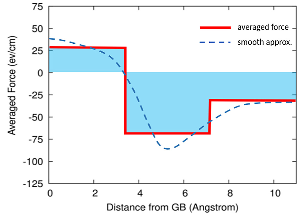
Figure 6. The regional-averaged force from Figure 5 as a function of the distance from the GB at E = 6.8 V/cm. The light blue blocks are the results from Figure 5 for the 3 regions. The red line shows the averaged force as a step function. The dashed blue curve is a smooth numerical approximation for the red step force. The figure was prepared using Gnuplot. GB: Grain boundary.
To further understand the reversal of the averaged EM force at the GB region demonstrated above, one needs to look at the change of electron conduction modes at the GB region. A comparison of mode resolved local electron density of states (DOS) between bulk and GB atoms is shown in Figure 7. Significant changes in both the s and p electron DOS are clearly seen. Due to the anisotropic nature of the p electrons, a significant shift in its fraction in conduction may lead to changes in the direction of the current-induced forces. Since the local DOS is well-known to be affected by atomic configurations near the GB[37], a change in the EM force on the GB atoms should be a common feature expected for various GB types in metals with a significant bulk EM force.
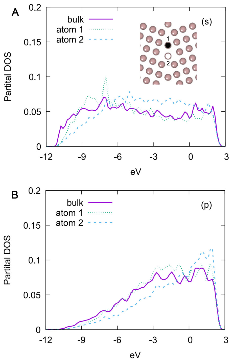
Figure 7. Comparison of the electron density of states between bulk and GB atoms. (A) For s electrons (shown on the top-right corner); (B) For p electrons (shown on the top-right corner). Positions of atom 1 and atom 2 on the GB are shown in the inset of (A) as black and white accordingly. The figure was prepared using Gnuplot. GB: Grain boundary.
It is also possible to present our EM force results based on electronic structure information like a valence charge density map near the GB since the EM force is simply the result of scattering-induced electron redistribution as seen from Eqns. 2 and 3. Since the purpose of this work is to highlight the importance of considering the current-induced force in microstructure evolution at the quantum mechanical level, instead of discussing the origin of the EM force, we choose to present the force directly.
Modelling GB motion using the coarse-grained force
The coarse-grained EM force near the GB from the previous section can be directly incorporated into the PFC model introduced in section 2.3 by constructing an effective potential
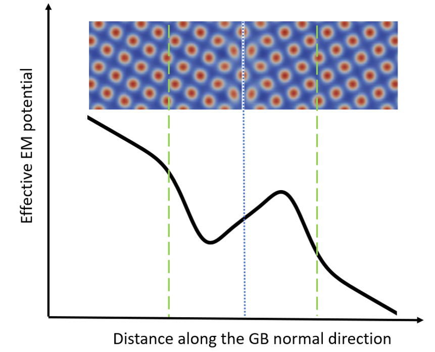
Figure 8. Illustration of the effective EM potential for the PFC model. The top inset picture is a PFC density field corresponding to the Σ5 GB and its vicinity, where atom positions are marked as red dots. The vertical dotted line marks the position of the GB, and the two dashed lines mark the boundaries of the near GB region, where the potential deviates significantly from its linear behavior in the bulk. The figure was prepared using Gnuplot. EM: Electromigration; GB: grain boundary; PFC: phase-field-crystal.
With the effective potential incorporated into the PFC model, the GB motion is demonstrated in Figure 9.
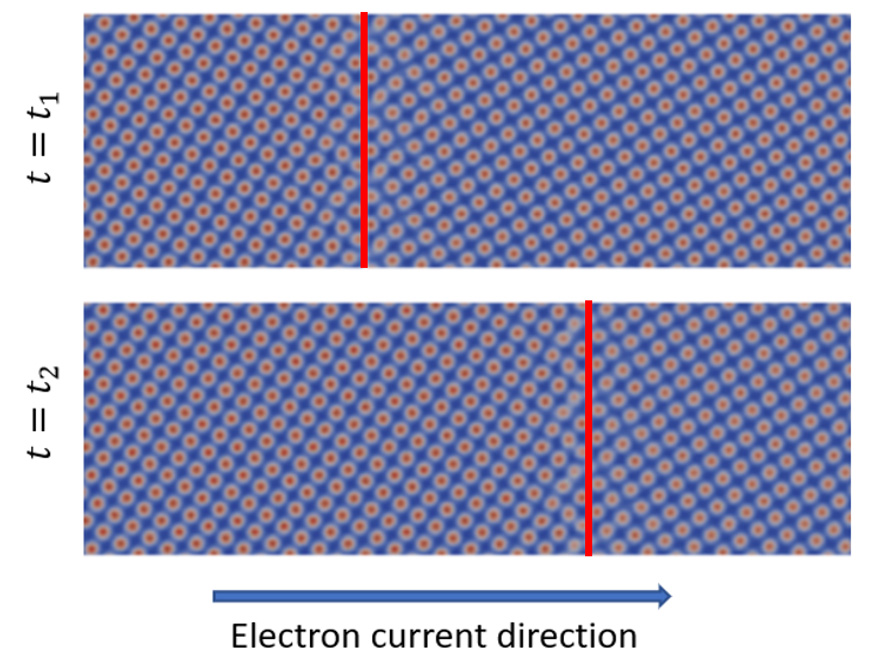
Figure 9. A demonstration of the electric current driven GB motion. The GB at time t = t1 was driven to move in the direction of electron current and reached the new position at t = t2. The GB positions are marked with red lines. The figure was prepared using Gnuplot. GB: Grain boundary.
Although a semi-quantitative EM force near the GB is used, the current driven GB motion demonstrated above is not close to quantitative yet. Despite the continuous effects in modelling GB migration processes, a general quantitative result at the mesoscale has not been achieved yet[40-42]. It has been shown that the GB mobility in the PFC model needs to be carefully calibrated in studies of GB migration[38]. Also, it is well-known that GB mobility depends sensitively on the system temperature. An electric current typically generates stronger Joule heating effect at the GB due to stronger electron scattering. A quantitative GB motion model should also take this heating effect into account. With all these efforts, one would still need the temperature dependent GB mobilities which requires intensive computational work[12,13]. It is noted that the current PFC model did not consider the temperature gradient or localized heating effects. Since the GB mobility used in the PFC model has not been calibrated, only a qualitative result in the GB motion is expected. Therefore, we did not use the more sophisticated PFC mode which incorporated the temperature gradient and local heating[43] in the current work.
Unlike other thermodynamic potentials used in driving the grain boundary motion where the potential takes two different constant values in the two grains, the thermodynamic potential constructed from the EM force in this work only becomes significant around the GB region and dies out to the same small bulk value in the two grains. When the potential takes two different values in the two grains, the exact transition behavior of the potential near the GB region may not be very important, but, as shown from our results, the exact potential form in the GB transition region becomes important in the EM case.
Regarding the in-depth analysis of the physical mechanism involved in this work, we would like to discuss it at the electronic scale and the GB motion scale separately since multiscale modelling is used in this work. At the electronic scale, the forces on atoms near the GB are calculated using the equations 2 and 3 based the electron wavefunctions obtained from standard quantum transport calculation. This is a well-established method for evaluating forces in quantum mechanical calculations, and it has been shown in both Figure 5 and the Supplementary Materials that this method reproduced the EM force in bulk Aluminum. At the GB motion scale, we turned to thermodynamics here by constructing an effective potential from the locally averaged EM force. The GB motion (or the associated materials transport) is the result of this effective potential. This is also a well-established approach used in both molecular dynamics and mesoscale modelling methods (see refs.[21,38]). One may question the bin range used in calculating the local averaged EM force, the one used in this work corresponds to the wavelength of conduction electrons at the Fermi level, this is an intrinsic length scale in the system and the average maintained some key features of the EM force near the GB while producing a smooth curve. Other choices of the bin range also have to be justified. This is the first attempt to model the current-induced GB motion from quantum mechanical EM forces, more sophisticated methods for effectively incorporating these forces into microstructure evolution models need to be developed in the future.
While the numerical results above predicted the motion direction of the Al Σ5 GB under a high electric current density, a possible experimental validation can be implemented as follows. The prepared pure Al polycrystalline sample should be annealed first to remove dislocations and residual stress. An electron backscatter diffraction (EBSD) measurement can be carried out to identify special GBs, then the sample can be prepared using focused ion beam (FIB). An expensive in-situ Transmission Electron Microscopy (TEM) under a large bias current density may identify the GB motion.
Although the local DOS results indicate that the EM force on GB atoms is expected to be different from the bulk, previous results on GB electron scattering[25] suggested that the Σ5 GB in Al has one of the highest electron reflection probability among several studied GB types in Al, Cu and Ag, therefore the reversal of the averaged EM force reported in this work should not be directly generalized to other GB types and metal systems.
CONCLUSIONS
In summary, this work carried out the first calculation of EM forces for atoms near a GB. A striking feature of the EM force near the symmetrical Σ5 tilt GB in Al is identified for the first time which leads to a motion of GB atoms in opposite direction from the bulk atoms under the electric current. An effective potential which reproduces the averaged EM force near the GB is constructed. GB motion consistent with the force calculations is demonstrated using a PFC based microstructure evolution model incorporated with an effective potential. Although the EM force calculation is performed for a single GB only, it brings up the necessity to carefully consider the current-induced forces at quantum mechanical level in modelling microstructure evolutions.
DECLARATIONS
Acknowledgments
The authors acknowledge the computer time support from the High Performance Computing Center of Guangdong Technion - Israel Institute of Technology. Su, X. and Wang, N. acknowledge the computation facility and technical support from HZW Technology, Shanghai.
Authors’ contributions
Simulation and data analysis: Su, X.; Xiao, Z.; Wang, N.
Conception and design of the study and manuscript writing: Wang, N.
Discussion and revision: Qi, Y.; Amouyal, Y.
Availability of data and materials
The raw data that support the findings of this study are available from the corresponding author upon reasonable request.
AI and AI-assisted tools statement
Not applicable.
Financial support and sponsorship
Qi, Y. acknowledges the National Natural Science Foundation of China Grant No 52471125, and Guangdong Province Science and Technology Major Project Grant No 2021B0301030005.
Conflicts of interest
All authors declared that there are no conflicts of interest
Ethical approval and consent to participate
Not applicable.
Consent for publication
Not applicable.
Copyright
© The Author(s) 2026.
Supplementary Materials
REFERENCES
1. Kim, M.; Bui-thi, T.; Kang, S.; Hong, S.; Nam Han, H. Electric current-induced phenomena in metallic materials. Curr. Opin. Solid. State. Mater. Sci. 2024, 32, 101190.
2. Sorbello, R. A pseudopotential based theory of the driving forces for electromigration in metals. J. Phys. Chem. Solids. 1973, 34, 937-50.
3. Dekker, J. P.; Lodder, A.; Van Ek, J. Theory for the electromigration wind force in dilute alloys. Phys. Rev. B. 1997, 56, 12167-77.
4. Lodder, A.; Dekker, J. P. The electromigration force in metallic bulk. In AIP Conference Proceedings; American Institute of Physics, 1998, 418, 315-28.
5. Tu, K. N. Recent advances on electromigration in very-large-scale-integration of interconnects. J. Appl. Phys. 2003, 94, 5451-73.
6. De Orio, R.; Ceric, H.; Selberherr, S. Physically based models of electromigration: from black’s equation to modern TCAD models. Microelectron. Reliab. 2010, 50, 775-89.
7. Liu, J.; Jia, D.; Fu, Y.; et al. Electroplasticity effects: from mechanism to application. Int. J. Adv. Manuf. Technol. 2023, 131, 3267-86.
8. Li, X.; Zhu, Q.; Hong, Y.; et al. Revealing the pulse-induced electroplasticity by decoupling electron wind force. Nat. Commun. 2022, 13, 6503.
9. Gu, S.; Kimura, Y.; Yan, X.; et al. Micromachined structures decoupling Joule heating and electron wind force. Nat. Commun. 2024, 15, 6044.
10. Xiang, Z.; Li, H.; Zhang, X.; Gao, P.; Zhan, M. Grain growth kinetics of a nickel-based superalloy under electric pulse treatment. Materials. 2025, 18, 2019.
11. Ceric, H.; Selberherr, S. Electromigration in submicron interconnect features of integrated circuits. Mater. Sci. Eng. R. Rep. 2011, 71, 53-86.
12. Bhate, D. N.; Kumar, A.; Bower, A. F. Diffuse interface model for electromigration and stress voiding. J. Appl. Phys. 2000, 87, 1712-21.
13. Chakraborty, S.; Kumar, P.; Choudhury, A. Phase-field modeling of grain-boundary grooving and migration under electric current and thermal gradient. Acta. Mater. 2018, 153, 377-90.
14. Liang, S. B.; Ke, C. B.; Wei, C.; Zhou, M. B.; Zhang, X. P. Phase field modeling of grain boundary migration and preferential grain growth driven by electric current stressing. J. Appl. Phys. 2018, 124, 175109.
15. Farmer, W.; Ankit, K. Phase-field simulations of electromigration-induced defects in interconnects with non-columnar grain microstructure. J. Appl. Phys. 2020, 127, 175301.
16. Clark, K. W.; Zhang, X. G.; Vlassiouk, I. V.; He, G.; Feenstra, R. M.; Li, A. P. Spatially resolved mapping of electrical conductivity across individual domain (grain) boundaries in graphene. ACS. Nano. 2013, 7, 7956-66.
17. Bevan, K. H.; Guo, H.; Williams, E. D.; Zhang, Z. First-principles quantum transport theory of the enhanced wind force driving electromigration on Ag(111). Phys. Rev. B. 2010, 81, 235416.
18. Bevan, K. H.; Zhu, W.; Stocks, G. M.; Guo, H.; Zhang, Z. Local fields in conductor surface electromigration: a first-principles study in the low-bias ballistic limit. Phys. Rev. B. 2012, 85, 235421.
19. Zhu, Q.; Cao, G.; Wang, J.; et al. In situ atomistic observation of disconnection-mediated grain boundary migration. Nat. Commun. 2019, 10, 156.
20. Schratt, A. A.; Mohles, V. Efficient calculation of the ECO driving force for atomistic simulations of grain boundary motion. Comput. Mater. Sci. 2020, 182, 109774.
21. Wang, N.; Ji, Y.; Wang, Y.; Wen, Y.; Chen, L. Two modes of grain boundary pinning by coherent precipitates. Acta. Mater. 2017, 135, 226-32.
23. Taylor, J.; Guo, H.; Wang, J. Ab initio modeling of quantum transport properties of molecular electronic devices. Phys. Rev. B. 2001, 63, 245407.
24. Feldman, B.; Park, S.; Haverty, M.; Shankar, S.; Dunham, S. T. Simulation of grain boundary effects on electronic transport in metals, and detailed causes of scattering. phys. stat. sol. (b). 2010, 247, 1791-6.
25. César, M.; Liu, D.; Gall, D.; Guo, H. Calculated resistances of single grain boundaries in copper. Phys. Rev. Appl. 2014, 2, 044007.
26. Hirel, P. Atomsk: A tool for manipulating and converting atomic data files. Comput. Phys. Commun. 2015, 197, 212-9.
27. Plimpton, S. Fast parallel algorithms for short-range molecular dynamics. J. Comput. Phys. 1995, 117, 1-19.
28. Mishin, Y.; Farkas, D.; Mehl, M. J.; Papaconstantopoulos, D. A. Interatomic potentials for monoatomic metals from experimental data andab initiocalculations. Phys. Rev. B. 1999, 59, 3393-407.
30. Tourret, D.; Liu, H.; Llorca, J. Phase-field modeling of microstructure evolution: recent applications, perspectives and challenges. Prog. Mater. Sci. 2022, 123, 100810.
31. Zhao, Y.; Xing, H.; Zhang, L.; et al. Development of phase-field modeling in materials science in China: a review. Acta. Metall. Sin. 2023, 36, 1749-75.
32. Mukherjee, A.; Ankit, K.; Mukherjee, R.; Nestler, B. Phase-field modeling of grain-boundary grooving under electromigration. J. Electron. Mater. 2016, 45, 6233-46.
33. Wang, N.; Guo, H.; Provatas, N. Connecting the phase-field-crystal model of electromigration with electronic and continuum theories. Phys. Rev. Materials. 2021, 5, 115002.
34. Perdew, J. P.; Wang, Y. Accurate and simple analytic representation of the electron-gas correlation energy. Phys. Rev. B. 1992, 45, 13244.
35. Olmsted, D. L.; Foiles, S. M.; Holm, E. A. Survey of computed grain boundary properties in face-centered cubic metals: I. Grain boundary energy. Acta. Mater. 2009, 57, 3694-703.
36. Zhang, Y.; Hong, Z.; Ye, Z.; Pan, X. Theoretical understanding of electromigration-related surface diffusion and current-induced force in Ag-Pd systems. ACS. Omega. 2024, 9, 29576-84.
37. Crampin, S.; Vvedensky, D. D.; MacLaren, J. M.; Eberhart, M. E. Electronic structure near (210) tilt boundaries in nickel. Phys. Rev. B. 1989, 40, 3413.
38. Xiao, Z.; Su, X.; Mordehai, D.; Wang, N. Controlling grain boundary mobility in phase-field-crystal model. Computational. Materials. Science. 2025, 253, 113869.
39. Fallah, V.; Korinek, A.; Ofori-opoku, N.; Provatas, N.; Esmaeili, S. Atomistic investigation of clustering phenomenon in the Al-Cu system: three-dimensional phase-field crystal simulation and HRTEM/HRSTEM characterization. Acta. Mater. 2013, 61, 6372-86.
40. Rohrer, G. S.; Chesser, I.; Krause, A. R.; et al. Grain boundary migration in polycrystals. Annu. Rev. Mater. Res. 2023, 53, 347-69.
41. Bhattacharya, A.; Shen, Y. F.; Hefferan, C. M.; et al. Grain boundary velocity and curvature are not correlated in Ni polycrystals. Science 2021, 374, 189-93.
42. Zhang, J.; Ludwig, W.; Zhang, Y.; et al. Grain boundary mobilities in polycrystals. Acta. Mater. 2020, 191, 211-20.
Cite This Article
How to Cite
Download Citation
Export Citation File:
Type of Import
Tips on Downloading Citation
Citation Manager File Format
Type of Import
Direct Import: When the Direct Import option is selected (the default state), a dialogue box will give you the option to Save or Open the downloaded citation data. Choosing Open will either launch your citation manager or give you a choice of applications with which to use the metadata. The Save option saves the file locally for later use.
Indirect Import: When the Indirect Import option is selected, the metadata is displayed and may be copied and pasted as needed.
About This Article
Special Topic
Copyright

Data & Comments
Data
0


Comments
Comments must be written in English. Spam, offensive content, impersonation, and private information will not be permitted. If any comment is reported and identified as inappropriate content by OAE staff, the comment will be removed without notice. If you have any queries or need any help, please contact us at [email protected].