


Numerical simulation and twinning evolution mechanism of the deep through silicon via electroplated copper
 0
0 Abstract
The microstructure is an important key factor for the reliability of deep through silicon via (TSV) electroplated copper. In the present study, the influence of current density on the surface physical field and microstructure in the electroplated copper were discussed using a combined method of numerical simulation and experiment. The results showed that the optimal electroplated parameters with the defect-free filling were confirmed to be at 0.1-0.17 Ampere per Square Decimeter (ASD) with an accelerator-to-suppressor ratio of 1:10 when the size of deep TSV was Φ20 μm × 200 μm with an aspect ratio of 10:1. The microstructure of TSVs exhibited a distinct distribution feature: fine grains along sidewalls and at the mouth, large columnar grains in mid-regions, and equiaxed grains at the bottom. The grain size and the quantity of Σ3 twin boundaries first decreased and then increased with increasing current density due to the competing effect of nucleation rate and grain growth by governing the polarization and suppressor desorption. Moreover, the intermediate 9R structure between the matrix and the twin was first observed in the electroplated copper, which provided a new way for strain accommodation in deep TSV electroplated copper, and the matrix→9R→twin pathway was proposed through the slip of Shockley partial dislocations. These findings served as a valuable reference for modeling microstructure evolution and laid a foundation for both microstructure prediction and control in deep TSV electroplated copper.
Keywords
INTRODUCTION
Through silicon via (TSV) filling, as a crucial interconnection method, can realize the vertical channels between chips and wafers by the electrodeposited copper, so it is critical for achieving high-density 3D integrated circuit packaging in the national defense and aerospace industries[1-3]. The technology development of the electrodeposited copper during TSV filling provides a possibility on allowing a substantial increase in the number of I/O connections, which in turn greatly enhances the semiconductor package performance[4,5].
As the packaging density increases, TSV dimensions are shrinking to the micro-nano scale[6]. Especially, the electrodeposited copper layer with a high aspect ratio of 10:1 makes that TSV technology has a great challenge, including incomplete filling, and defects like voids and gaps. Additionally, the microstructure of electrodeposited copper layer becomes extremely non-uniform due to a high aspect ratio, and the non-uniform microstructure causes a negative effect on the reliability and performance of interconnection[7,8]. Therefore, these phenomena of micro-nano scale effect, electrochemical deposition defect and non-uniform microstructure make that a number of researchers use the established model, numerical simulation and electroplating experiment to solve above-mentioned problems.
For instance, Wang et al. proposed a novel three-component model considering the additive systems (accelerator, suppressor, and leveler) to simulate the TSV filling process at different current densities, while the diameter and depth of the TSV was 20 μm × 65 μm, and the aspect ratio was 3.25:1[9]. Tao et al. studied the effect of additives (accelerator, suppressor) and chloride ions (Cl-) on the TSV filling at the aspect ratios of 2:1 (90 μm × 180 μm, 50 μm × 100 μm) and 10:1 (10 μm × 100 μm) through the combined method of numerical simulation and experiment[10]. Wang et al. investigated the effect of current density on the copper filling within the deep TSV electroplated copper with high aspect ratio of 10:1 (20 μm × 200 μm) through electrochemical deposition experiments[11]. It was concluded that TSV filling results mainly had three morphologies. At the low current density (less than 1 mA·cm-2), TSV filling results were free of defects. At the medium current density (between 2 and 5 mA·cm-2), TSV filling results had seam defects. At the high current density (greater than 6 mA·cm-2), TSV filling results had void defects. Zhang et al. utilized electron back-scattered diffraction (EBSD) technique to investigate the microstructure and texture of electrodeposited Cu micro-cylinders in the blind hole with a diameter of 40 µm and a depth of 140 µm, and pointed put that the preferred orientation of the Cu overburden film changed from {111} to {220} when the current density increased from 2 to 80 mA·cm-2[12].
Moreover, it is crucial to reveal the evolution mechanism of microstructure for the deep TSV electroplated copper layer for establishing microstructure evolution models during the electrodeposition process, as well as for improving the reliability and property of interconnections. Hasegawa et al. prepared the nanotwinned copper foils with a high texture by means of pulse electroplating, and pointed out that the twin orientation could be altered from the horizontal to vertical direction by adjusting the growth potential[13]. Lu et al. discovered the alternating distribution of 9R structure and twins in Face-Centered Cubic (FCC) through systematic high-resolution scanning transmission electron microscopy (TEM) analysis, clarifying the nucleation and evolution process of 9R structure and twins in FCC materials during high-temperature annealing[14]. Bezzola et al. employed numerical simulation to investigate the nucleation and growth mechanism during the electrodeposition process, comprehensively considering various influence factors, combining the microscale nucleation model and the macroscale current distribution model to predict the deposition thickness[15]. Xu et al. investigated the relationship between the microstructure and property of copper alloys under different processing conditions, and clarified the effect of dislocations on the strength and toughness of copper alloys[16].
In the present work, the influence of applied current density on the deep TSV electroplated copper with a high aspect ratio of 10:1 and microstructure morphology of Cu are investigated using a combination method of numerical simulation (COMSOL Multiphysics field software) and electrodeposited experiment. A three-component model considering the additive systems (accelerator, suppressor) to simulate the TSV filling process at different current densities is established. And, electron backscatter diffraction (EBSD) characterization, focused ion beam/scanning electron microscopy (FIB/SEM), transmission Kikuchi diffraction (TKD) technology, and TEM are used to observe the evolution of twin and grain morphology. The matrix→9R→twin pathway is observed and discussed, and the reason for grain morphology evolution from column grain to equiaxed grain is revealed.
MATERIAL AND METHODS
Method and model of numerical simulation
In this study, the electrodeposited module of COMSOL Multiphysics software was used to simulate the deep TSV filling process, employing the Arbitrary Lagrangian-Eulerian (ALE) approach. The finite element model, considering the processes of diffusion, adsorption, and desorption of additives (including the accelerator and suppressor) and Cl- was developed[10]. It was assumed that the mass transport of ion, described using the Nernst-Planck equation, was mainly dominated by the diffusion and electro-migration ignoring the convection. Moreover, the current density on the cathode surface could be divided into three parts: the current density ia from the surface covered by the accelerator, the current density is from the surface covered by the suppressor, and the current density iu from the uncovered surface. The current density was calculated using a Butler-Volmer equation which was taking into consideration the effect of additives to calculate local plating current density[9]. The numerical simulation was carried out at the current densities of 0.05, 0.07, 0.09, 0.1, 0.15, 0.17, 0.2 Ampere per Square Decimeter(ASD) (1 ASD = 100 A·m-2) and the ratios of accelerator and suppressor concentration 1:1, 1:5, 1:10. According to the present numerical simulation [Supplementary Figures 1 and 2], the optimal electrodeposited parameters had been confirmed at the ranges from 0.1-0.17 ASD and an optimal ratio of accelerator and suppressor concentration 1:10. The void-free deep TSV filling experiment [Supplementary Figure 3] could be achieved at the optimal electrodeposited parameter ranges that are used to verify the validation of simulation. The experimental results show good agreement with the simulated results described above, which further confirms the reliability of the simulation and the accuracy of the model.
The current density was set at 0.1, 0.15, and 0.17 ASD (1 ASD = 100 A·m-2) using a direct current power supply. The electrolyte composition consisted of CuSO4, H2SO4, Cl-, with a fixed accelerator [Bis-(sodium sulfopropyl)-disulfide, SPS]-to-suppressor (polyethylene glycol, PEG) concentration ratio of 1:10. The total deposition time in the simulation was determined by the experimental complete filling time. All simulations were performed at a constant temperature of 25 °C. The geometric model and mesh division for the deep TSV electroplated copper are shown in Figure 1.
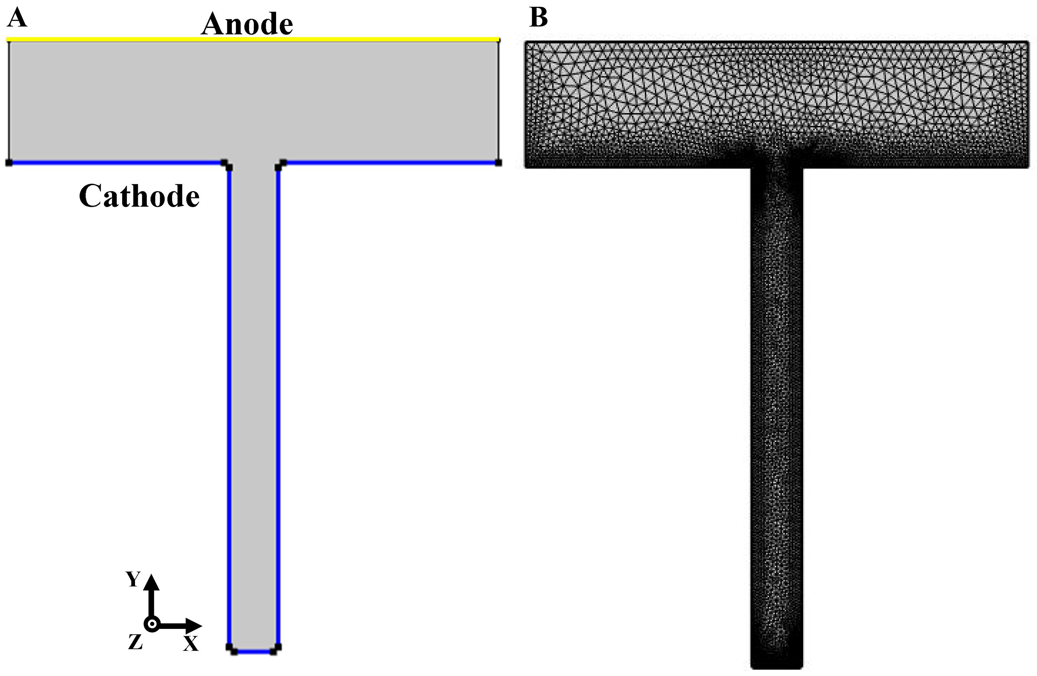
Figure 1. (A) Two-dimensional model and (B) grid division model of the deep TSV electroplated copper. TSV: Through silicon via.
In this model, the electrode surface reactions primarily involve three key complexes: PEG-Cl--Cu2+, SPS-Cl--Cu2+, and free Cu2+. The model focuses on capturing the behavior of these complexes, with their transport and reaction kinetics governed by mass conservation laws. Furthermore, the influence of current density on their behavior at the electrode surface is analyzed through energy conservation principles. The specific physical framework is presented in the following section.
The substance transport in the electrolyte is governed by the Nernst-Planck equation, and the fluxes of substance (Ni) are expressed as follows[9]:
where Ni is the fluxes of substance (mol·m-2·s-1), Di is the diffusion coefficient of the additive or ion (m-2·s-1), Ci is the concentration of the additive or ion (mol·m-3), zi is the number of valence electrons, Φ is the potential in the electrolyte solution (V), µi is the mobility constant, F is the Faraday constant, and u is the velocity field governed by the incompressible Navier-Stokes equations (m·s-1).
The diffusion process is governed by Fick’s second law, with the temporal variation of copper ion concentration due to the concentration gradient at a given location described by Eq. (2). The electromigration process involves the movement of charged copper ions under the influence of an electric field, with the corresponding temporal variation of copper ions given by Eq. (3). The Nernst-Einstein equation relates the diffusion and electromigration of copper ions[9], as shown in Eq. (4).
where R is the universal gas constant (8.314 J·K-1·mol-1), T is the temperature (298 K), ▽2 is the Laplace operator, and µCu2+ is the electrochemical mobility of copper ions (m2·V-1·s-1).
Since the additives are the electro-neutral with the neglection of the electromigration process, and their transport in the electrolyte is governed solely by Fickian diffusion, as described by Eq. (5):
According to the research on the additives by Akolkar et al., the concentration of additives on the electrode surface directly affects their coverage rate on the electrode surface[22]. Considering the effect of the diffusion, adsorption and desorption of three substances (accelerator, suppressor and Cl-) on the cathode surface, the surface coverage rates of three substances are expressed using Eqs. (6-8) based on the Langmuir adsorption equation[9].
Where θA, θCl-, and θP denote the surface coverages (%) of the accelerator, Cl-, and suppressor, respectively,
Based on the behavior of additives at the electrode surface, the adsorption reaction rate (Eq. 9) and the adsorption-desorption kinetics (Eq. 10) are defined to establish the equilibria among the normal fluxes of the accelerator, suppressor, and Cl- from the electrolyte to the deposition interface:
where Ri is the adsorption reaction rate of the additive (mol·m-2·s-1), Radi is the net adsorption-desorption reaction rate (mol·m-2·s-1), ki+ and ki- is the adsorption and desorption rate constant, respectively, and Γi is the surface saturation concentration of the additive (mol·m-2).
In the present model, the current density associated with this process is described by the Butler-Volmer equation and is given by:
where
Since the electrodeposition process occurs exclusively at the cathode, the anodic contribution to the current density is neglected. The cathodic current density is therefore governed by Eqs. (12-14), which determines the total deposition rate at the electrode surface.
where
The total deposition current density is composed of the current contributions from the accelerator-covered surface (iA), the suppressor-covered surface (iP), and the additive-free surface (ifree), and is expressed as[9]:
The deposition rate is governed by the local current density. According to Faraday’s law, the relationship between current density and deposition rate can be described as:
where MCu is the molar mass of copper (0.06355 kg·mol-1),
The parameters for numerical simulation during the filling process of the deep TSV electroplated copper are summarized in Table 1.
| Symbol | Value | Units | Symbol | Value | Units |
| D(Cl-) | 9 × 10⁻¹⁰ | m2·s-1 | kcl | 20 | m3·mol-1·s-1 |
| D(Cu2+) | 2.65 × 10⁻¹⁰ | m2·s-1 | kcl | 1.5 × 10⁷ | 1·m-1 |
| D(P) | 1 × 10⁻¹⁰ | m2·s-1 | kA | 50 | m3·mol-1·s-1 |
| D(A) | 1 × 10⁻⁸ | m2·s-1 | kA | 3.5 × 10² | 1·m-1 |
| ГP | 9.2 × 10⁻⁸ | mol·m-2 | αP | 0.6 | / |
| ГA | 8 × 10⁻⁷ | mol·m-2 | αA | 0.4 | / |
| ГCl- | 1.62 × 10⁻⁵ | mol·m-2 | αc | 0.3 | / |
| kp | 2,500 | m3·mol-1·s-1 | T | 298 | K |
| kp | 1 × 10⁷ | 1·m-1 | n | 2 | / |
Electrodeposition experiment
A CZ300 machine was utilized as the direct current electrodeposited equipment. As shown in Figure 2A, the sample size was 10 mm × 10 mm for the deep TSV electroplated copper layer. The copper layer was electrodeposited on the silicon substrate. Figure 2B shows the top view of the via arrangement and the via spacing is 60 μm. The size of deep TSV is approximately Φ20 μm × 200 μm with an approximate aspect ratio of 10:1, as shown in Figure 2C. Figure 2D schematically depicts the multilayer material composition of the TSV cross-section. The multilayer structure consists of SiO2 as the insulating layer, Ti as the barrier layer, and Cu as the seed layer. The seed layer has a thickness of 1 μm, and copper is electroplated to fill the TSV. The essential raw materials for deep TSV electroplated copper include a base electrolyte solution and additives. The primary additive system is a sulfuric acid-based electrolyte system, consisting of an accelerator (SPS), a suppressor (PEG), and Cl-. According to the optimal electrodeposited parameters (0.1-0.17 ASD and a ratio of accelerator and suppressor concentration 1:10) that are preliminary confirmed by the numerical simulation, the electrodeposition experiment is carried out.
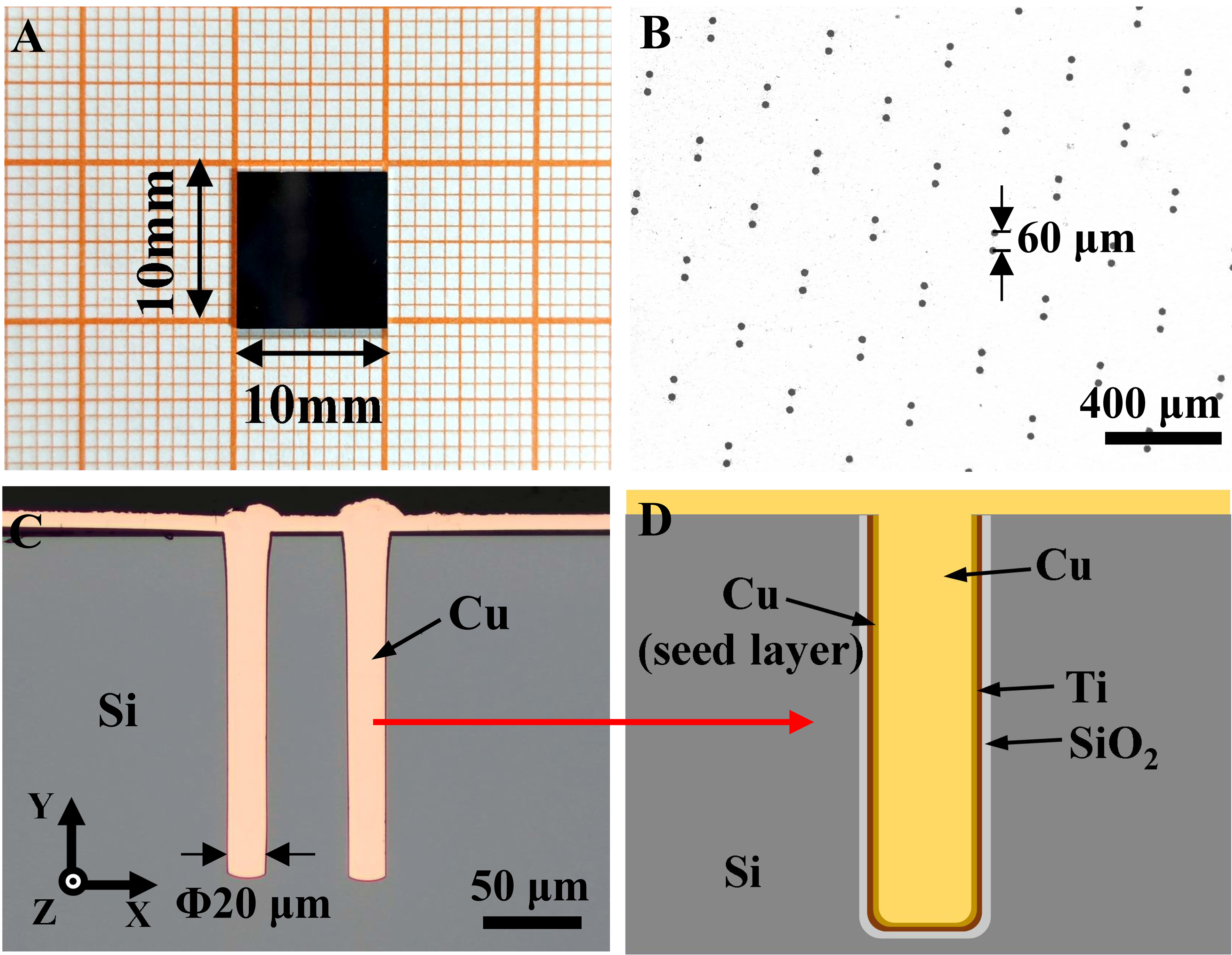
Figure 2. Deep TSV electroplated copper: (A) TSV sample; (B) via arrangement; (C) section of TSV; (D) schematic diagram of multi-player material for TSV. TSV: Through silicon via.
Microstructure characterization
The surface filling of the deep TSV electroplated copper layer at different magnifications was observed using Leica DMI3000M Optical Microscope (OM). EBSD was performed to quantify the microstructural parameters, including grain size, twin boundary, and the distribution of low-angle and high-angle grain boundaries. The TEM samples were fabricated using Helios G4 CX FIB/SEM, and the FEI Talos F200X field emission high-resolution transmission electron microscope was utilized for TEM observations. The TKD technique was employed to characterize and analyze the morphology of columnar and equiaxed grains of the deep TSV electroplated copper layer.
RESULTS AND DISCUSSION
Effect of current density on the simulated deep TSV filling
Figure 3 shows the numerical simulation results of electrochemical deposition process for the deep TSV electroplated copper with an additive concentration ratio of 1:10 (accelerator concentration: suppressor concentration) and an applied current density of 0.15 ASD. As shown in Figure 3A, the via filled at 0.15 ASD exhibits no detectable electrolyte potential, confirming that defect-free filling is achieved. Each electrolyte potential curve in Figure 3B represents the simulated filling morphology at different electrodeposition times, exhibiting a characteristic V-shaped filling profile during the deposition process. The V-shaped filling profile is corresponding to the defect-free filling confirmed by the electrochemical deposition experiments in the following section.
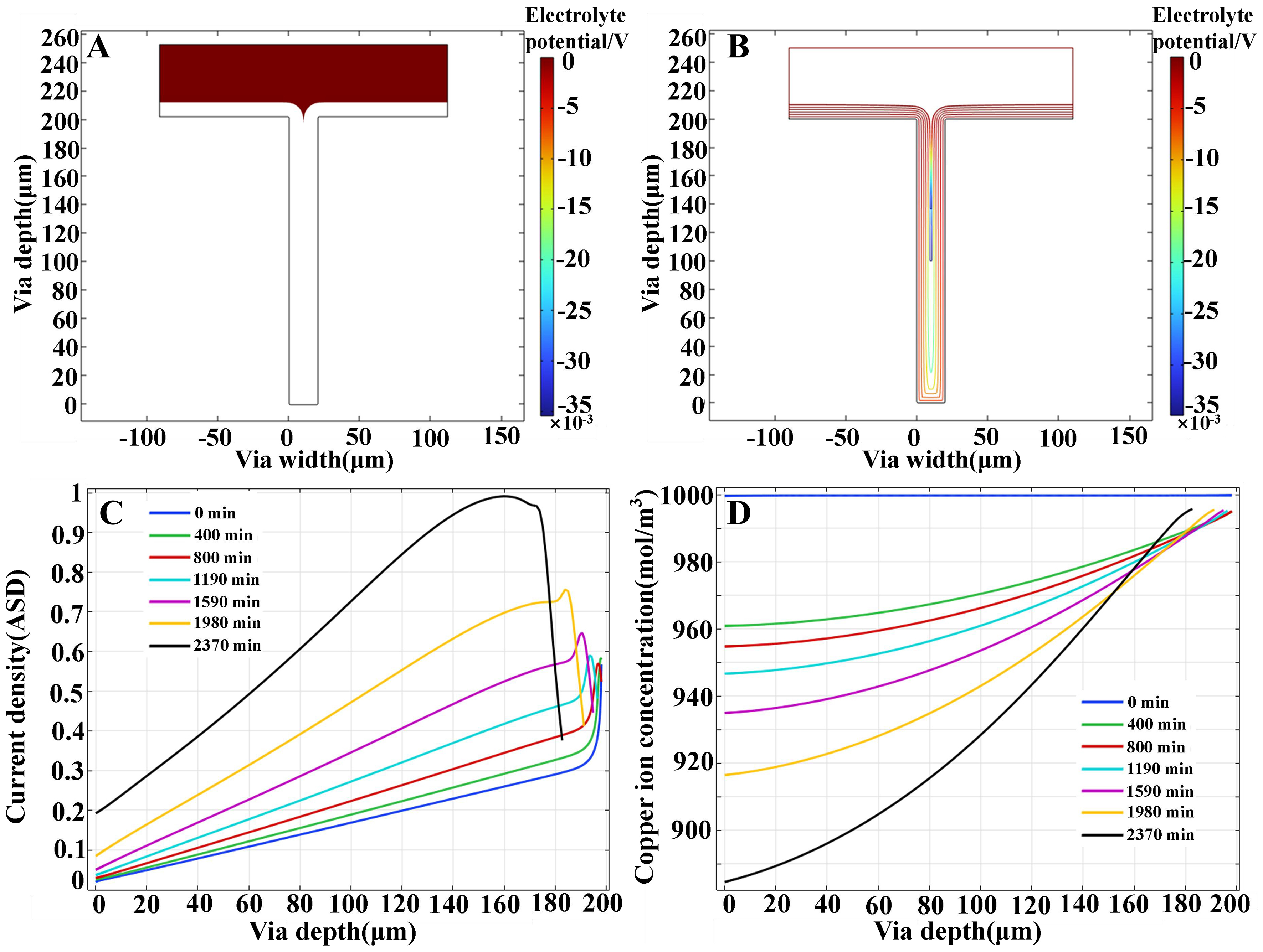
Figure 3. Simulation results of deep TSV electroplated copper at an additive concentration ratio of 1:10 and a current density of 0.15 ASD: (A) the electrolyte potential distribution after filling showing the defect-free filling result; (B) the electrolyte potential distribution at different electrodeposition times; (C) the current density distribution along the via depth at different electrodeposition times; (D) the distribution of copper ion concentration along the via depth at different electrodeposition times. TSV: Through silicon via; ASD: ampere per square decimeter.
Figure 3C shows the distribution of current density along the via depth direction at different electrodeposition times. It can be observed that the variation trend of current density is different at different electrodeposited stages. In the early stage of electrodeposition, as indicated by the blue and green curves, the highest current density appears at the via mouth, whereas the lowest occurs at the bottom. In contrast, during the later stage, the maximum current density shifts to a depth of 150 µm, as shown by the black curve. This phenomenon implies that the maximum of local current density shifts toward the via middle-top region during TSV electrodeposited copper. Figure 3D shows the evolution of copper ion concentration distribution in the deep TSV electroplated copper at 0.15 ASD. A noticeable concentration gradient develops from the lowest concentration of via bottom to the highest concentration of via mouth with the electrodeposition time. At the beginning of electrodeposition, the copper ion concentration is uniformly maintained at
Effect of current density on the microstructure of the deep TSV electroplated copper
In order to systematically demonstrate the changes in the microstructure during the bottom-up filling process of deep TSV electroplated copper, the electro-deposited copper layer is divided into four distinct regions (I, II, III, IV) along the electrodeposition V-shaped filling process, as shown in the Figure 4. The following analysis describes the evolution of copper grains according to this regional sequence, providing a clear framework for understanding the grain morphology and size distribution from the via bottom to the top. Figure 4 shows the effect of current density on the inverse pole figure (IPF) of the deep TSV electroplated copper at an additive concentration ratio of 1:10. As shown in Figure 4A, a fine-grained layer forms on the via walls (region I) because the pre-deposited copper seed layer provides abundant nucleation sites for subsequent electrodeposition. In the region away from the via wall, the microstructure is consisted of equiaxed and columnar grains (region II). Notably, the grain colors in the IPF map indicate that the grains exhibit random crystallographic orientations without any distinct texture. In the early stage of electrodeposition, the microstructure is mainly consisted of coarse and equiaxed grains at the via bottom. As the electrodeposition goes on, the columnar grain grows along the via diameter direction at the middle region of the via (region III), and the microstructure is composed of fine and equiaxed grains at the via mouth (region IV). Moreover, the microstructure of four distinct regions is quantitatively analyzed, as shown in Figure 5. In Figure 5A and B, the Cu grain size first increases and then decreases along the electrodeposition direction. The result of aspect ratio is good agreement with the observation of microstructure morphology in Figure 4. The observed changes in grain size can be rationalized using electrocrystallization theory, with the electrodeposition kinetics expressed by the following equation[24]:
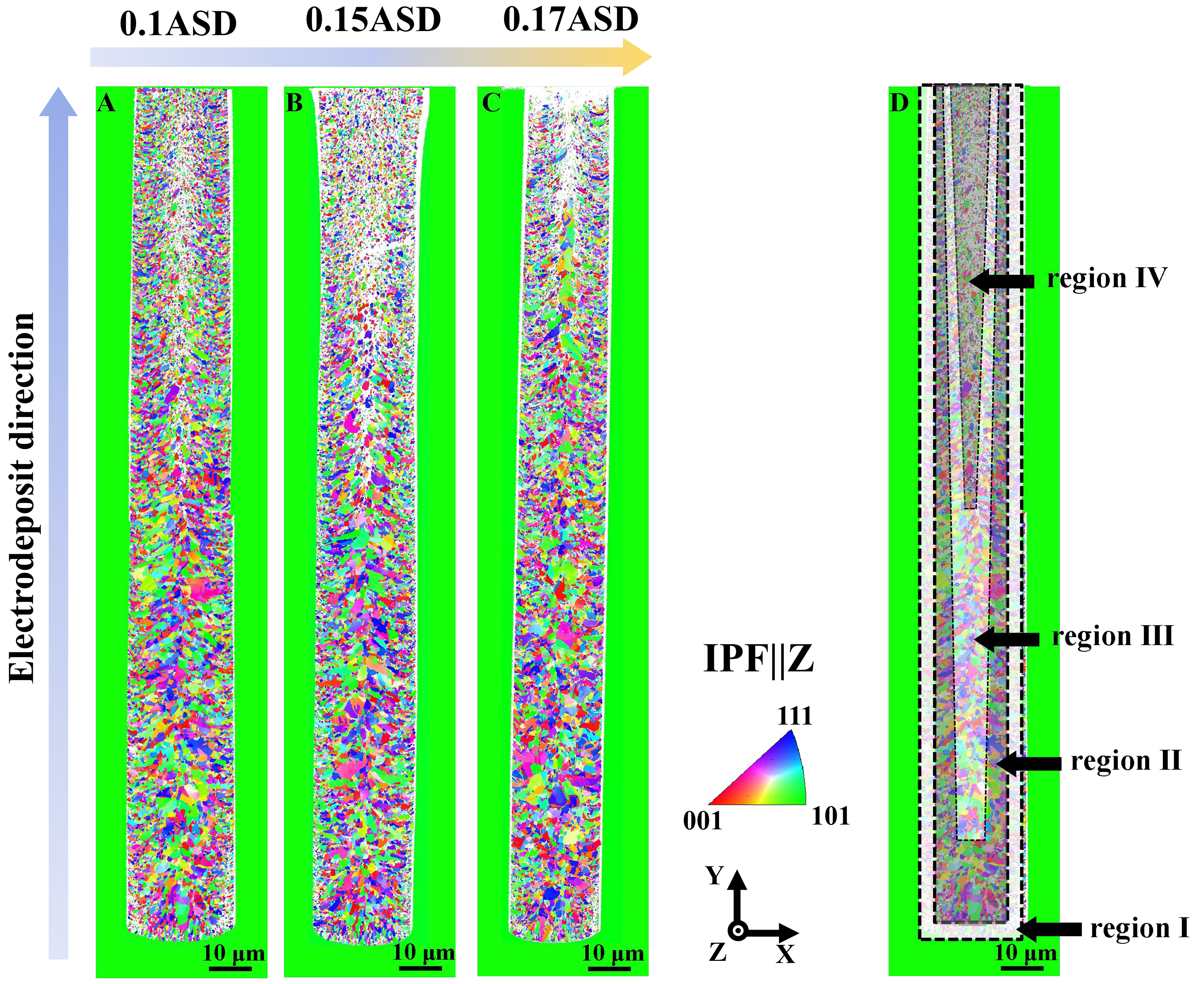
Figure 4. Effect of current density on the IPF ||Z of the deep TSV electroplated copper at an additive concentration ratio of 1:10: (A) 0.1 ASD; (B) 0.15 ASD; (C) 0.17 ASD; (D) regional division diagram. IPF: Inverse pole figure; ASD: ampere per square decimeter.
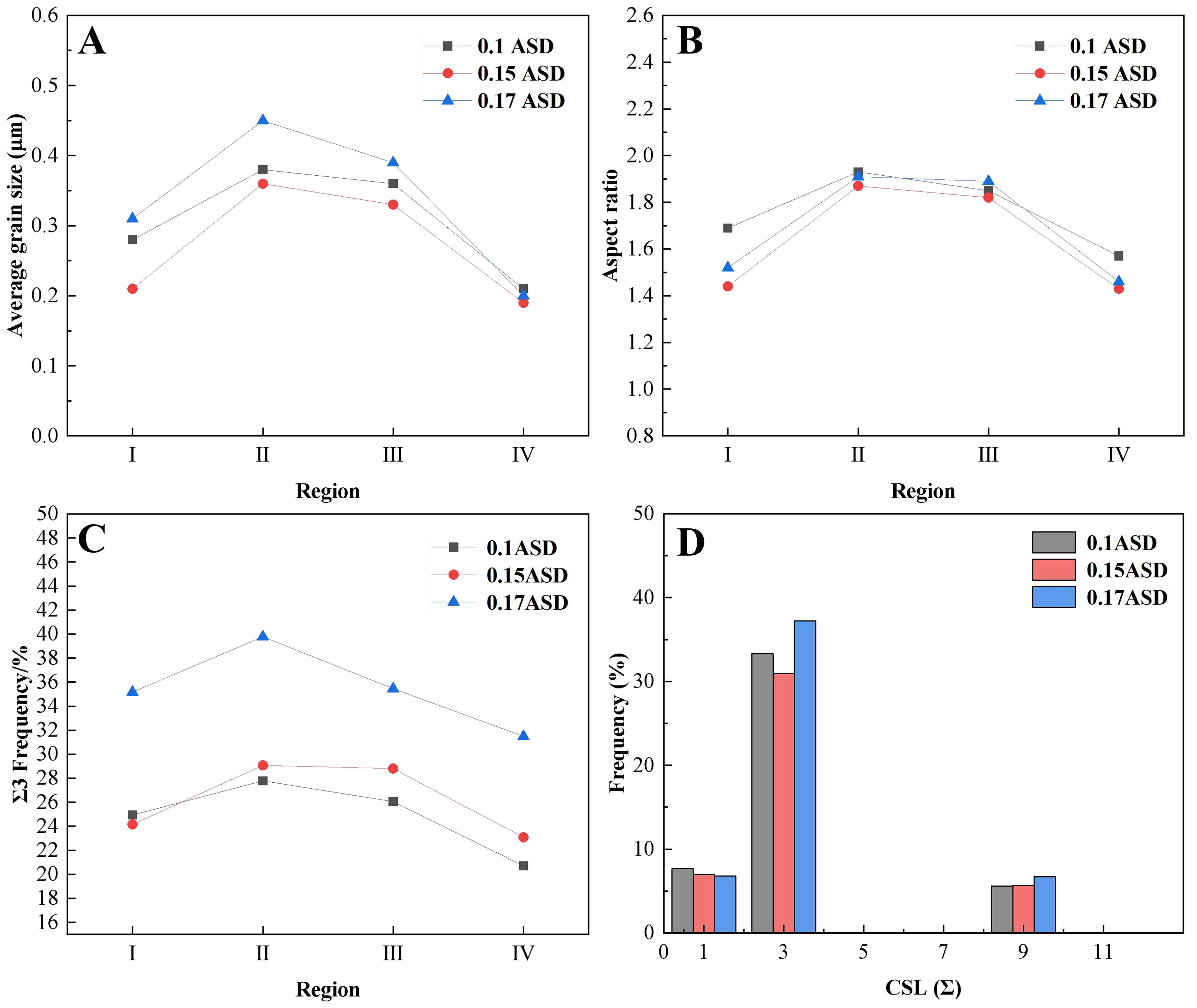
Figure 5. Effect of current density on the microstructure at different regions of deep TSV and an additive concentration ratio of 1:10: (A) average grain size; (B) aspect ratio of grain; (C) frequency of Σ3 twin boundaries; (D) frequency of all twin boundaries. TSV: Through silicon via.
where η is the cathode potential (V), I is the current density (ASD), a and b are the chemical constants, W is the nucleation rate (%), B is a material constant, and T is the temperature (K).
It can be deduced from Eq. (17) that the cathode potential η increases with increasing current density I. From Eq. (18), the nucleation rate W increases exponentially with increasing cathode potential η. Therefore, a higher current density I corresponds to a higher nucleation rate W, finally resulting in finer Cu grains. According to the above simulation results, the current density at the via mouth is 0.4 ASD in the early stage of electrodeposition but it is 0.1 ASD at the via bottom. Therefore, the higher nucleation rate at the via mouth leads to a fine grain distribution in region IV, whereas the lower nucleation rate at the via bottom produces coarser grains in regions II and III. During electrodeposition, the peak current density moves toward the via’s middle-top region, enhancing the growth rate and driving dynamics of Cu grain nuclei along the direction of the steep current density gradient. Concurrently, a higher accelerator (SPS) concentration in the via’s middle-bottom region promotes the formation of columnar grains in the middle region (regions II and III).
From Figure 5A, it can be also seen that the size of Cu grain first decreases and then increases in the middle region (regions II and III) and via wall (region I) as the current density increases, but there is a negligible effect on the size of Cu grain at the mouth region (region IV). Thus, an overall coarsening tendency of Cu grains is observed at a current density of 0.17 ASD. This behavior can be attributed to the fact that increasing current density strengthens the polarization effect, thereby enhancing Cu nucleation and favoring the formation of fine grains. However, when the current density exceeds a critical threshold, the suppressor undergoes desorption from its inhibited state to an uninhibited state, accelerating grain growth and resulting in coarser Cu grains[25].
In the deep TSV electroplated copper, Σ3 and Σ9 twins are present, with Σ3 coincident site lattice (CSL) boundaries dominating. Figure 5C shows the variation trend of Σ3 twin grain boundaries along the deposition direction at different current densities. It is present that the density of Σ3 twin grain boundaries initially increases and then decreases along the deposition direction. Furthermore, as shown in Figure 5D, the density of Σ3 twin grain boundaries first decreases and then increases with increasing current density, which is similar to the size change of Cu grain, and it can be inferred that the twin density is positively correlated with the grain size.
To further investigate the grain morphology characteristics of the deep TSV electroplated copper, a TKD characterization is performed on region II of Figure 4A at a current density 0.1 ASD and an additive concentration ratio of 1:10, as shown in Figure 6. Figure 6A reveals a mixed microstructure with columnar and equiaxed grains. According to the above-mentioned simulation results of this electrodepositing area, the current density at the via wall is 0.6 ASD but it is 0.2 ASD at the via’s middle region, a larger gradient of current density exists between the via wall and the central axis, causing that copper grain growth is dominated over nucleation in the early electrodeposition stage. Consequently, columnar grains form along the electric field lines under these conditions. During electrodeposition, the current density gradient diminishes while the overall current density increases, leading to an enhanced nucleation but suppressed grain growth. As a result, fine equiaxed grains develop along the central axis of the via [Figure 6A]. Figure 6B and C reveals the high density of Σ3 twin boundaries and the local misorientation map, respectively. From Figure 6C, an obvious accumulation of geometrically necessary dislocations (GNDs) occurs at the twin boundaries in region Ⅱ. The observation region can be divided into zone I and zone II based on the density of Σ3 twin boundaries in Figure 6B. As shown in Figure 6D and E, the density of Σ3 twin boundaries, defined as the fraction of Σ3 twin boundary length relative to the total grain boundary length, reaches 36.31% in the columnar-grain region and 34.44% in the equiaxed-grain region. This further verifies the positive correlation between grain size and twin boundary density.
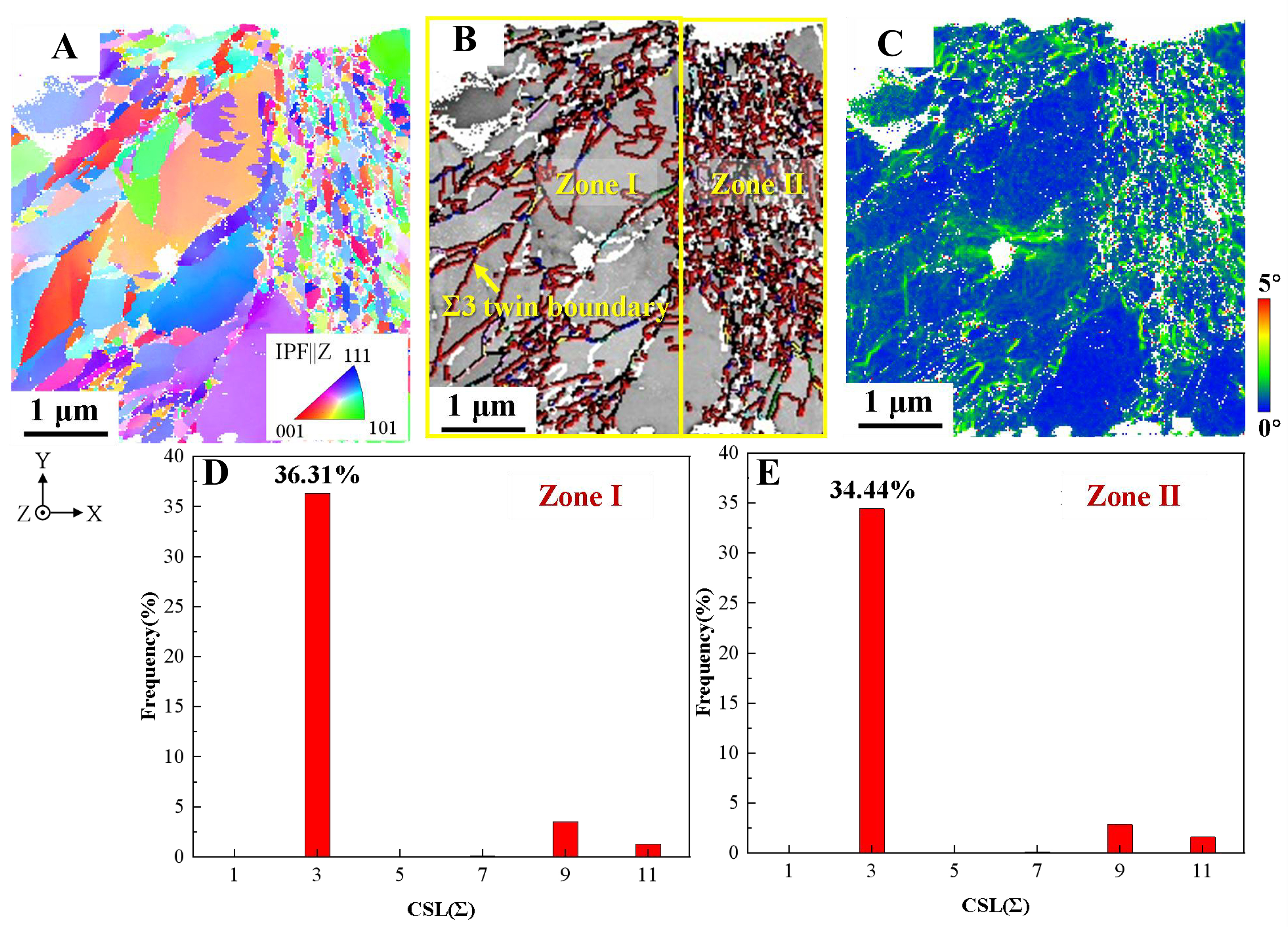
Figure 6. TKD results of region II in Figure 4A at a current density of 0.1 ASD and an additive concentration ratio of 1:10: (A) IPF||Z image; (B) band contrast and boundary distribution map; (C) KAM map;(D) twin boundary distribution of zone I in Figure 6B; (E) twin boundary distribution of zone II in Figure 6B. TKD: Transmission Kikuchi diffraction; IPF: inverse pole figure; KAM: kernel average misorientation; ASD: ampere per square decimeter.
Σ3 twin characteristics in the deep TSV electroplated copper
As mentioned above, the Σ3 twin boundary is frequently observed in the deep TSV electroplated copper. As shown in Supplementary Figure 5, numerous Σ3 twin boundaries are detected near the sidewall of the deep TSV electroplated copper at a current density of 0.1 ASD and an additive concentration ratio of 1:10. Two characteristic twin morphologies are highlighted: one consists of twins partially extending through the grain [Supplementary Figure 5D], and the other consists of twins fully extending through the grain [Supplementary Figure 5E]. These twins are Σ3 twins (i.e. {111}<
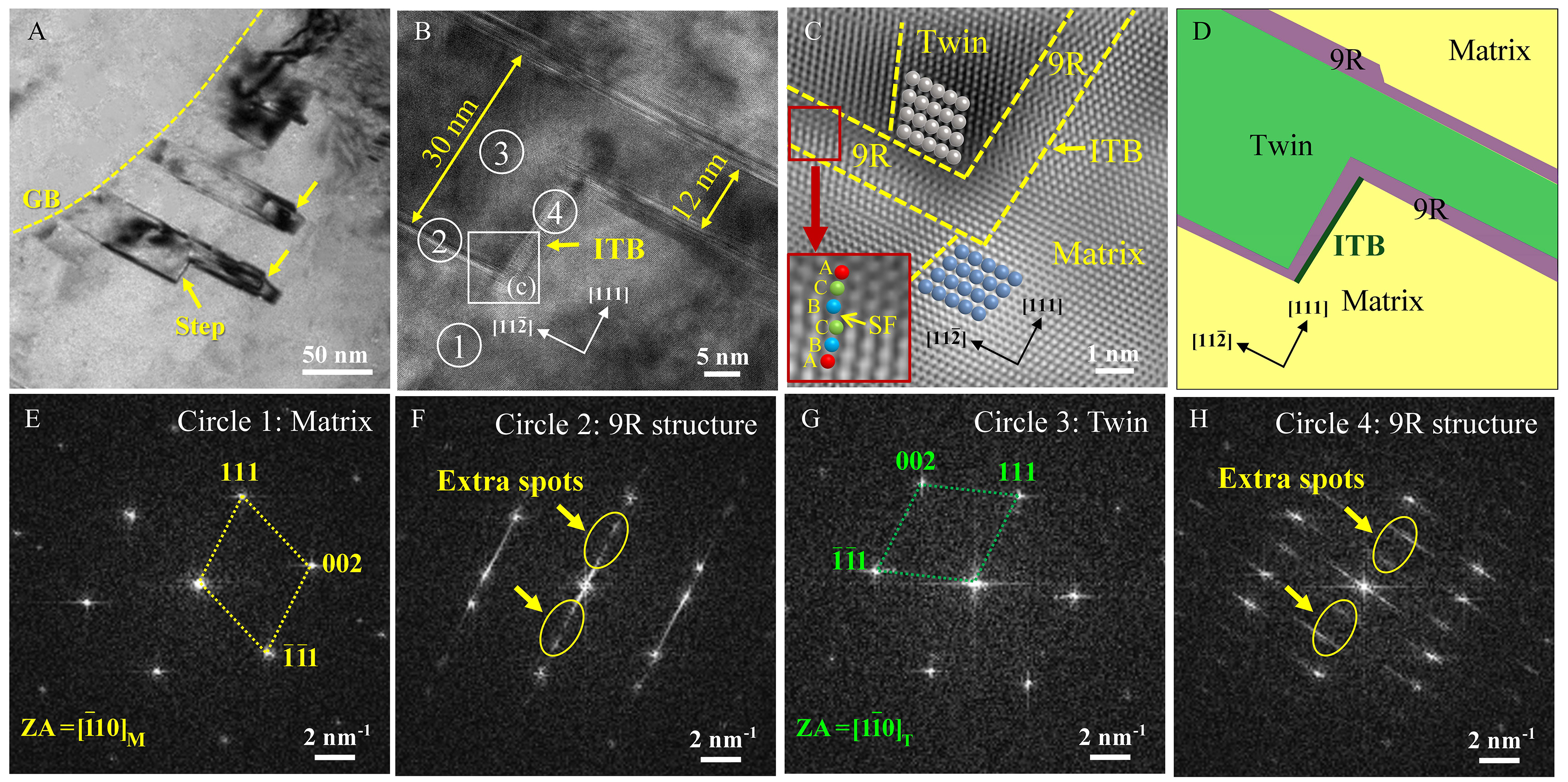
Figure 7. TEM results of twins with a stepped morphology partially extending through the grain: (A) BF image; (B) HRTEM image; (C) IFFT image of the region marked by the white square in (B); (D) structural distribution map of (B); (E-H) FFT images of the regions marked by white circles 1-4 in (B). BF: Bright field; HRTEM: high-resolution transmission electron microscopy; IFFT: inverse fast Fourier transform; FFT: fast Fourier transform; ITB: incoherent twin boundary; GB: grain boundary; SF: stacking fault; ZA: zone axis; M: matrix.
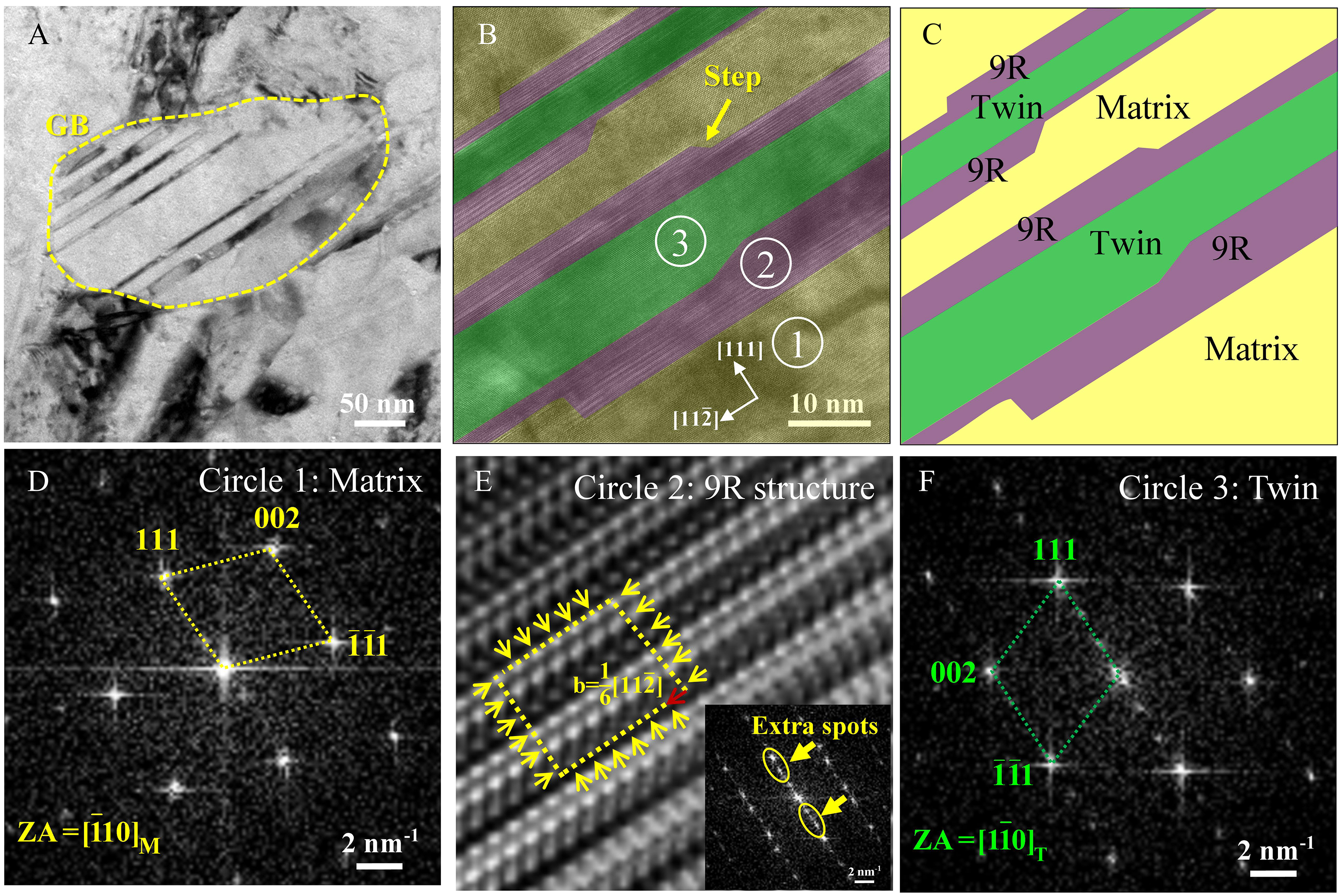
Figure 8. TEM results of twins fully extending through the grain: (A) BF image; (B) HRTEM image showing steps near the twins; (C) structural distribution map of (B); (D) FFT images of the region marked by white circle 1 in Figure 8B; (E) IFFT and FFT images of the region marked by white circle 2 in Figure 8B; (F) FFT image of the region marked by white circle 3 in Figure 8B. BF: Bright field; HRTEM: high-resolution transmission electron microscopy; FFT: fast Fourier transform; IFFT: inverse fast Fourier transform; GB: grain boundary; ZA: zone axis.
Figure 7 shows twins partially extending through the grain. As shown in Figure 7A, the twins originate from the grain boundary and extend into the interior of the grain. Several steps are observed at the front of the twins. As shown in Figure 7B, the twin consists of two laths with thicknesses of 30 and 12 nm, forming a step, indicating that these two twin segments are formed sequentially from left to right. Besides, a periodic structure appears next to the twin and parallel to (111) and (
The twins fully extending through the grain are shown in Figure 8. The structural distribution map in Figure 8C is also obtained based on the FFT results. In Figure 8A, although no steps are observed in the BF image, both the HRTEM image [Figure 8B] and the structural distribution map [Figure 8C] reveal the presence of steps within the 9R structure. The matrix/9R interface and the 9R/twin interface, both parallel to the (111) plane, together with the steps within the 9R structure, indicate that the 9R structure and twins are formed layer by layer along the (111) plane, and the steps serve as the boundary between the transformed and untransformed regions. As shown in Figure 8E, a dislocation with Burgers vector of
Discussion
Formation mechanism of Σ3 twin in the deep TSV electroplated copper
The reason for the formation of the 9R structure prior to twinning
According to the above result, the 9R structure forms prior to twinning, and both the 9R structure and twins develop layer by layer. Figure 9 shows the stacking sequence along [111] direction among FCC matrix, twins of different thicknesses and 9R structure. The stacking sequence of the FCC structure is ABC|ABC|ABC (A, B and C respectively represent the arrangement of atoms at different levels on the corresponding crystal planes). As the number of atomic layers increases from 1 to 6, it is observed that the stacking sequence within the twin zone (marked in green in Figure 9) is BAC|BCA. Specifically, in Figure 9A, for twins containing 1-, 3-, 4-, and 6-layer atoms, the stacking sequence above the topmost twin plane differs from that of the FCC matrix. For instance, the stacking sequence above the topmost twin plane of the 6-layer twin is BCA, whereas the corresponding rows in the FCC matrix follow the ABC sequence. This indicates that the formation of twins containing 1-, 3-, 4-, and 6-layer atoms induces lattice distortion in the FCC matrix due to the differing stacking sequences. As shown in Figure 9B, twins containing 2- and 5-layer atoms do not produce stacking sequences different from those of the matrix above the twin zone. In fact, twins containing (2 + 3n) atomic layers do not alter the stacking sequence above the twin zone either, where n is a natural number. However, the layer-by-layer formation of atomic planes during twinning implies that the number of atomic layers in the twin zone cannot be limited to only 2-, 5-, or (2 + 3n). Therefore, a transitional stacking structure is required to accommodate the transformation.
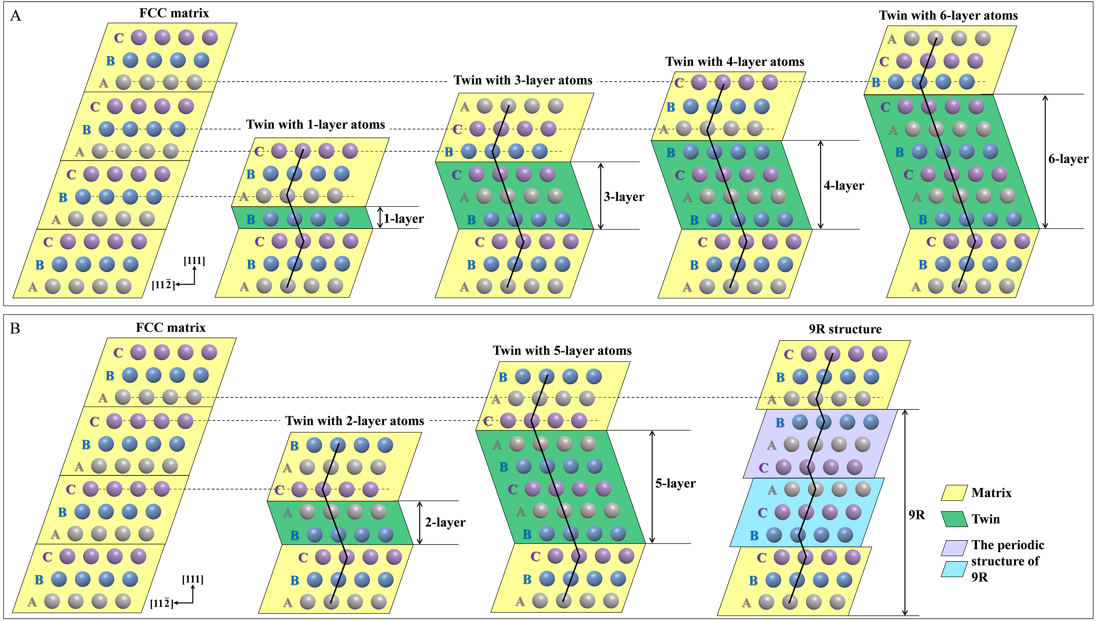
Figure 9. Comparison of stacking sequence along [111] direction among the FCC matrix, twins of different thicknesses and 9R structure: (A) stacking sequence above the twin plane of 1-, 3-, 4-, and 6-layer twins, differing from that of the FCC matrix; (B) stacking sequence above the twin plane of 2- and 5-layer twins or above the faulted planes of the 9R structure, matching that of the FCC matrix. The first row of atoms above the topmost twin plane of the twins or above the topmost faulted plane of the 9R structure, along with the corresponding atoms in the matrix, is marked with horizontal dashed lines. FCC: Face-centered cubic.
The formation of the 9R structure prior to twinning rationalizes this issue. As shown in Figure 9B, the stacking sequence of the 9R structure is ABC|BCA|CAB. The stacking sequence above the 9R zone is ABC, the same as that of the matrix, and does not induce lattice distortion in the matrix above the topmost faulted planes. Thus, the prior formation of the 9R structure ensures that twins can grow with minimal lattice distortion in the surrounding matrix.
The structural transformation process during matrix→9R→twin
During the formation of the 9R structure and twins, Shockley partial dislocations with a Burgers vector of
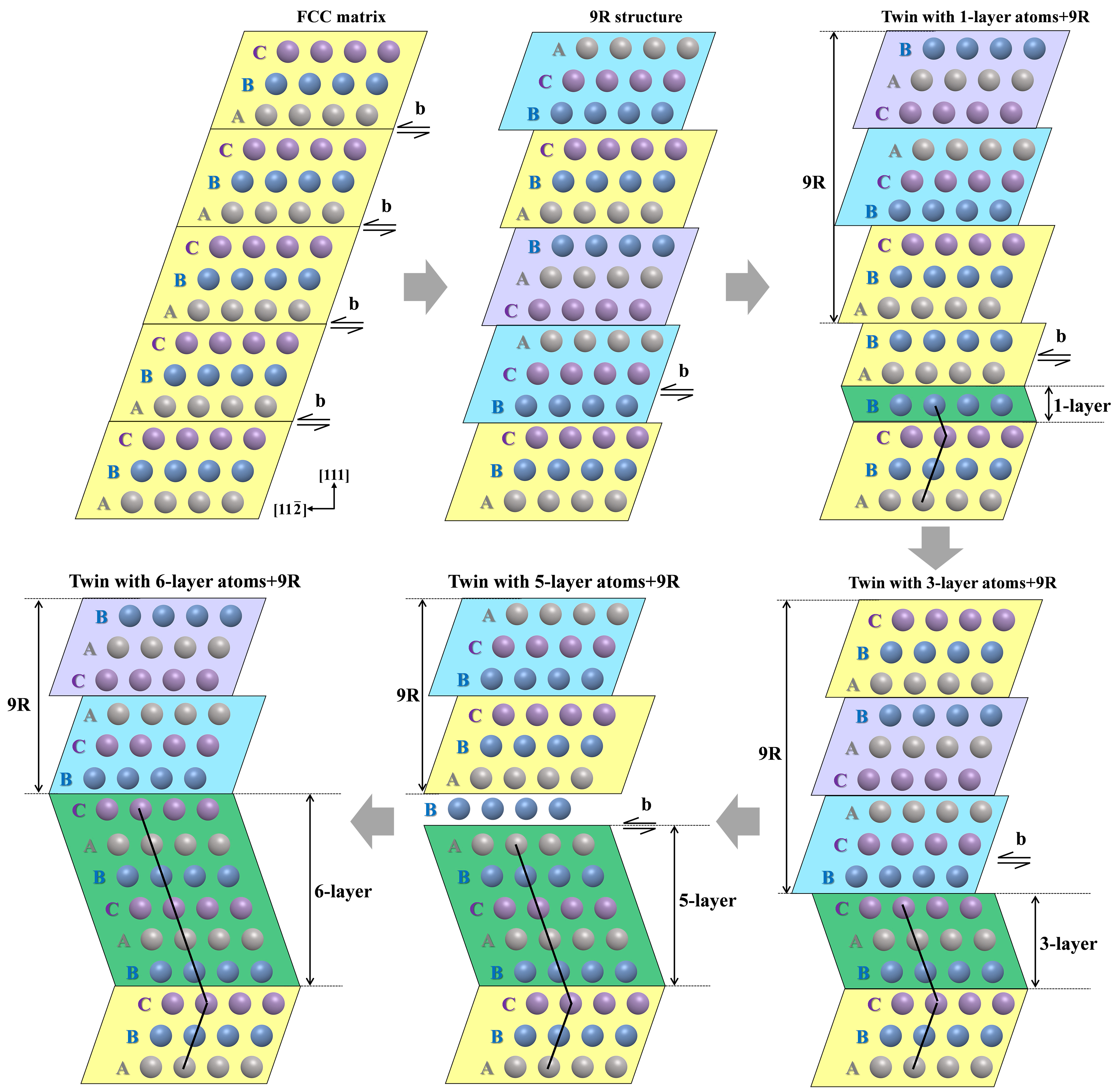
Figure 10. Schematic illustration of the matrix→9R→twin transformation process, showing that under the action of Shockley partial dislocations, the introduction of the 9R structure prior to twinning can lead to twin thickening and upward migration of the 9R structure. FCC: Face-centered cubic.
The observation of an intermediate 9R structure in deep TSV electroplated copper differs markedly from previous reports on electrodeposited or magnetron-sputtered Cu films[18-21]. The deep TSV electrodeposition involves high aspect ratio, for example, 10:1 in this work. Although the filling quality is good [Supplementary Figure 3B-D], the geometrical confinement induces pronounced overpotential gradient [Supplementary Figures 1 and 2], resulting in highly non-equilibrium condition for crystal growth at different time and locations. This is supported by the different grain size at the different locations in Figure 4. Under the combined effect of overpotential gradients and geometrical confinement, particularly in regions near the upper part of the TSV (indicated by the blue potential profile in Supplementary Figure 2E), grain nucleation occurs more frequently. This leads to finer grains, which are required to accommodate larger local strains owing to strain accommodation among a greater number of grains. In this context, the formation of an intermediate 9R structure provides a new pathway for strain accommodation, enabling its persistence in these regions. This finding enriches the existing twinning theory of copper and demonstrates that highly non-equilibrium conditions under geometrical confinement can activate additional metastable structure.
Evolution of grain morphology in the deep TSV electroplated copper
Figure 11 shows the microstructural evolution of the deep TSV electroplated copper at a current density of 0.1 ASD and an additive concentration ratio of 1:10. As shown in Figure 11A, three distinct microstructural regions are identified from sidewall to central axis: (i) surface fine-grained zone (< 500 nm grain size); (ii) intermediate columnar grain zone (1-3 μm width); and (iii) central equiaxed grain zone (2-5 μm diameter). Specifically, fine and columnar grains dominate near the sidewalls, while equiaxed grains predominantly occupy the central region.
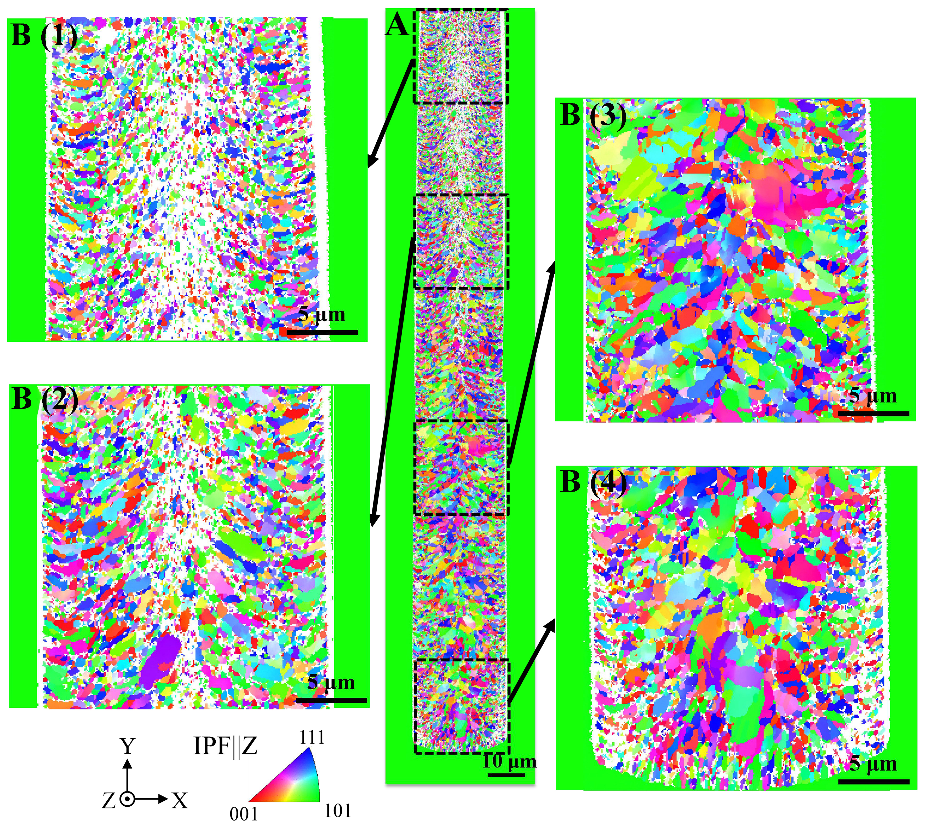
Figure 11. Microstructure and morphology of the deep TSV electroplated copper at a current density of 0.1 ASD and an additive concentration ratio of 1:10: (A) IPF||Z image; (B1-B4) local magnification of (A). TSV: Through silicon via; IPF: inverse pole figure; ASD: ampere per square decimeter.
Along electrodeposit direction, four regions with different grain morphology are identified. In Figure 11B (4), the grain morphology in the bottom area of the via is predominantly equiaxed grains, with fine grains near the via sidewall. The grains on the sidewall grow laterally and those in the central area grow vertically upward. In the lower-middle area of the via [Figure 11B (3)], the grains on the sidewall are columnar and exhibit an oblique upward growth trend, while the grains in the central area are equiaxed. In the upper-middle area of the via [Figure 11B (2)], the grains on the sidewall are columnar and grow obliquely upward, and the grains in the central area are fine equiaxed. At the via opening area [Figure 11B (1)], the grains on the sidewall are fine and columnar, growing laterally, and the grains in the central area are fine equiaxed.
This structural gradation originates from the interplay of three electroplating mechanisms: liquid-phase mass transfer, electron transfer, and phase formation. Notably, accelerator and inhibitor additives critically regulate copper grain nucleation and growth dynamics. Accelerators preferentially adsorb at the via bottom, reducing cathodic polarization to enhance Cu2+ reduction and grain growth. Conversely, inhibitors concentrate at the via opening, increasing cathodic polarization to suppress both Cu2+ reduction and nucleation. Spatial heterogeneity in current density and Cu2+ concentration induces coupled electrochemical and concentration polarization effect. Both electrochemical polarization and concentration polarization jointly impact the electrocrystallization process. Electrochemical polarization enhances nucleation density through increased overpotential, yielding refined-grain copper layer. Concentration polarization governs grain growth kinetics by modulating local ion availability, directly affecting coating uniformity and density. As demonstrated in Section 3.1, bottom-to-top deposition progression correlates with current density variation: minimal at the via bottom versus maximal at the opening [Figure 3C]. Consistent with electrocrystallization principles, higher current density at the opening promotes elevated nucleation rates, resulting in dense nuclei formation. Simultaneously, electric field alignment at the bottom facilitates directional growth along field lines, fostering columnar grain development. With prolonged electroplating, inhibitor depletion near the opening shifts the dominant mechanism from growth to nucleation. Spatial confinement coupled with homogenized polarization conditions restricts grain growth in central regions, ultimately stabilizing equiaxed microstructures. Therefore, inhibitor concentration and overpotential emerge as critical parameters governing intraluminal nucleation-growth equilibria. However, the current model does not take into account the influence of convection, which will limit the material transport process and result in low accuracy of the copper ion concentration field. In subsequent research, a convection model will be further incorporated to more clearly elucidate the microstructure evolution mechanism.
CONCLUSIONS
The influence of applied current density on physical fields and microstructure evolution during the filling process of deep TSV electroplated copper is investigated in the present study. In combination with the numerical simulation and the microstructural observation, the twinning mechanism and grain morphology evolution of deep TSV electroplated copper are discussed. The main conclusions are as follows:
(1) The defect-free filling is achieved at 0.1-0.17 ASD with an accelerator-to-suppressor ratio of 1:10 when the size of deep TSV is approximately Φ20 μm × 200 μm with an approximate aspect ratio of 10:1. Numerical simulations reveal that the local current density peak shifts from the via mouth toward the middle-top region as electrodeposition proceeds, accompanied by copper ion depletion at the via bottom.
(2) Microstructural analysis demonstrates a distinct grain distribution: fine grains along sidewalls and at the mouth, large columnar grains in mid-regions, and equiaxed grains at the bottom. Both grain size and Σ3 twin boundary density exhibit a non-monotonic dependence on current density, governed by competing nucleation and growth effect under polarization and suppressor desorption.
(3) The intermediate 9R structure between the matrix and the twin are first observed in electroplated copper, and the atomic-scale evolution of the matrix→9R→twin mechanism is proposed to occur via the slip of Shockley partial dislocations. This process minimizes lattice distortion and enables coordinated 9R migration along the [111] direction during twin thickening, accounting for the stepped twin growth morphology and providing a new pathway for strain accommodation in deep TSV electroplated copper.
DECLARATIONS
Acknowledgments
We also thank Dr. Kengfeng Xu for his valuable assistance with the microstructural analysis.
Authors’ contributions
Design: Wei, J.
Experiments: Wei, J.
Data analysis: Wei, J.
Manuscript writing: Wei, J.; Luo, J.; Wu, D.
Manuscript revision and supervising: Luo, J.; Wu, D.
Availability of data and materials
The data supporting the findings of this study are available from the corresponding author upon reasonable request.
AI and AI-assisted tools statement
Not applicable.
Financial support and sponsorship
The authors acknowledge the support from the Key R&D Program of Shaanxi Province (Grant No. 2024CY2-GJHX-32), the National Natural Science Foundation of China (Grant No. 52475406), and Ye Qisun Science Foundation of National Natural Science Foundation of China (Grant No. U2341254).
Conflicts of interest
All authors declared that there are no conflicts of interest.
Ethical approval and consent to participate
Not applicable.
Consent for publication
Not applicable.
Copyright
© The Author(s) 2026.
Supplementary Materials
REFERENCES
1. Tian, W.; Li, Z.; Wang, Y.; Zhang, G. Height uniformity simulation and experimental study of electroplating gold bump for 2.5D/3D integrated packaging. Micromachines 2022, 13, 1537.
2. Cui, H.; Tian, W.; Zhang, Y.; Chen, Z. The study of the reliability of complex components during the electromigration process. Micromachines 2023, 14, 499.
3. Shen, W. W.; Chen, K. N. Three-dimensional integrated circuit (3D IC) key technology: through-silicon via (TSV). Nanoscale. Res. Lett. 2017, 12, 56.
4. Park, S.; Chun, B.; Kim, S.; Kim, H.; So, H. Microstructural analysis and design of electroplated-Cu micropillar under different process variables and pattern structures. Mater. Des. 2025, 252, 113715.
5. Li, W.; Li, Z.; Zeng, F. Y.; et al. Cu pillar electroplating using a synthetic polyquaterntum leveler and its coupling effect on SAC305/Cu solder joint voiding. Materials 2024, 17, 5405.
6. Singh, N.; Srivastava, K.; Kumar, A.; et al. Challenges and opportunities in engineering next-generation 3D microelectronic devices: improved performance and higher integration density. Nanoscale. Adv. 2024, 6, 6044-60.
7. Zhang, M.; Qin, F.; Chen, S.; et al. Holding time effect on mechanical properties and protrusion behaviors of through silicon via copper under various annealing processes. Mater. Sci. Semicond. Process. 2023, 158, 107353.
8. Tang, S.; Chen, J.; Hu, Y. B.; et al. Brief overview of the impact of thermal stress on the reliability of through silicon via: analysis, characterization, and enhancement. Mater. Sci. Semicond. Process. 2024, 183, 108745.
9. Wang, F.; Zhao, Z.; Wang, F.; Wang, Y.; Nie, N. A novel model for through-silicon via (TSV) filling process simulation considering three additives and current density effect. J. Micromech. Microeng. 2017, 27, 125017.
10. Tao, Y.; Liang, C.; Mei, Z.; et al. Numerical simulation of copper electrodeposition for through silicon via (TSV) with SPS-PEG-Cl additive system. Microelectron. J. 2024, 144, 106089.
11. Wang, F.; Wang, F.; Liu, X.; Liu, J. Experimental study of current density in copper filling process within deep through-silicon vias with high aspect ratio. J. Micromech. Microeng. 2019, 29, 125013.
12. Zhang, Y.; Ding, G.; Wang, H.; Cheng, P. Microstructure of electrodeposited Cu micro-cylinders in high-aspect-ratio blind holes and crystallographic texture of the Cu overburden film. J. Mater. Sci. Technol. 2016, 32, 355-61.
13. Hasegawa, M.; Mieszala, M.; Zhang, Y.; Erni, R.; Michler, J.; Philippe, L. Orientation-controlled nanotwinned copper prepared by electrodeposition. Electrochim. Acta. 2015, 178, 458-67.
14. Lu, W.; An, F.; Liebscher, C. H. Detwinning/twin growth-induced phase transformation in a metastable compositionally complex alloy. Microstructures 2022, 2, 17.
15. Bezzola, A.; Bales, B. B.; Petzold, L. R.; Alkire, R. C. Numerical scaling studies of kinetically-limited electrochemical nucleation and growth with accelerated stochastic simulations. J. Electrochem. Soc. 2014, 161, E3001-8.
16. Xu, X.; Tong, X.; Wu, G.; Zhang, L. Ameliorating the microstructure and mechanical properties of Al-Cu-Li alloy through aging temperature in a novel thermo-mechanical treatment. Microstructures 2025, 5, 2025089.
17. Grujicic, D.; Pesic, B. Electrodeposition of copper: the nucleation mechanisms. Electrochim. Acta. 2002, 47, 2901-12.
18. Lu, L.; Chen, X.; Huang, X.; Lu, K. Revealing the maximum strength in nanotwinned copper. Science 2009, 323, 607-10.
19. Chen, P.; Shen, W.; Chen, Z.; et al. Surface atom migration-involved two-dimensional nucleation and growth of nanotwinned copper in DC electrodeposition. Acta. Mater. 2024, 262, 119468.
20. Zhang, X.; Wang, H.; Chen, X. H.; et al. High-strength sputter-deposited Cu foils with preferred orientation of nanoscale growth twins. Appl. Phys. Lett. 2006, 88, 173116.
21. Fan, C.; Xie, D.; Li, J.; et al. 9R phase enabled superior radiation stability of nanotwinned Cu alloys via in situ radiation at elevated temperature. Acta. Mater. 2019, 167, 248-56.
22. R., Landau, U. Mechanistic analysis of the “bottom-up” fill in copper interconnect metallization. J. Electrochem. Soc. 2009, 156, 351-5.
23. Braun, T. M.; Josell, D.; John, J.; Moffat, T. P. Editors’ choice - simulation of copper electrodeposition in through-hole vias. J. Electrochem. Soc. 2019, 167, 013510.
24. Lui, G.; Chen, D.; Kuo, J. EBSD characterization of twinned copper using pulsed electrodeposition. J. Phys. D. Appl. Phys. 2009, 42, 215410.
25. Atanasova, T. A.; Strubbe, K.; Vereecken, P. M. Adsorption/desorption of suppressor complex on copper: description of the critical potential. ECS. Trans. 2011, 33, 13-26.
26. Li, Q.; Song, J.; Liu, G.; Liu, Y.; Wang, J.; Zeng, X. Migration kinetics of twinning disconnections in nanotwinned Cu: an in situ HRTEM deformation study. Scr. Mater. 2021, 194, 113621.
27. Han, J.; Wu, Y.; Zhao, K.; Wang, H.; Liu, S.; Liu, X. Effects of controlling grain growth mode on microstructures and properties of Cu foil. J. Mater. Res. Technol. 2023, 24, 2018-27.
Cite This Article
How to Cite
Download Citation
Export Citation File:
Type of Import
Tips on Downloading Citation
Citation Manager File Format
Type of Import
Direct Import: When the Direct Import option is selected (the default state), a dialogue box will give you the option to Save or Open the downloaded citation data. Choosing Open will either launch your citation manager or give you a choice of applications with which to use the metadata. The Save option saves the file locally for later use.
Indirect Import: When the Indirect Import option is selected, the metadata is displayed and may be copied and pasted as needed.
About This Article
Special Topic
Copyright

Data & Comments
Data
0


Comments
Comments must be written in English. Spam, offensive content, impersonation, and private information will not be permitted. If any comment is reported and identified as inappropriate content by OAE staff, the comment will be removed without notice. If you have any queries or need any help, please contact us at [email protected].