


fig8
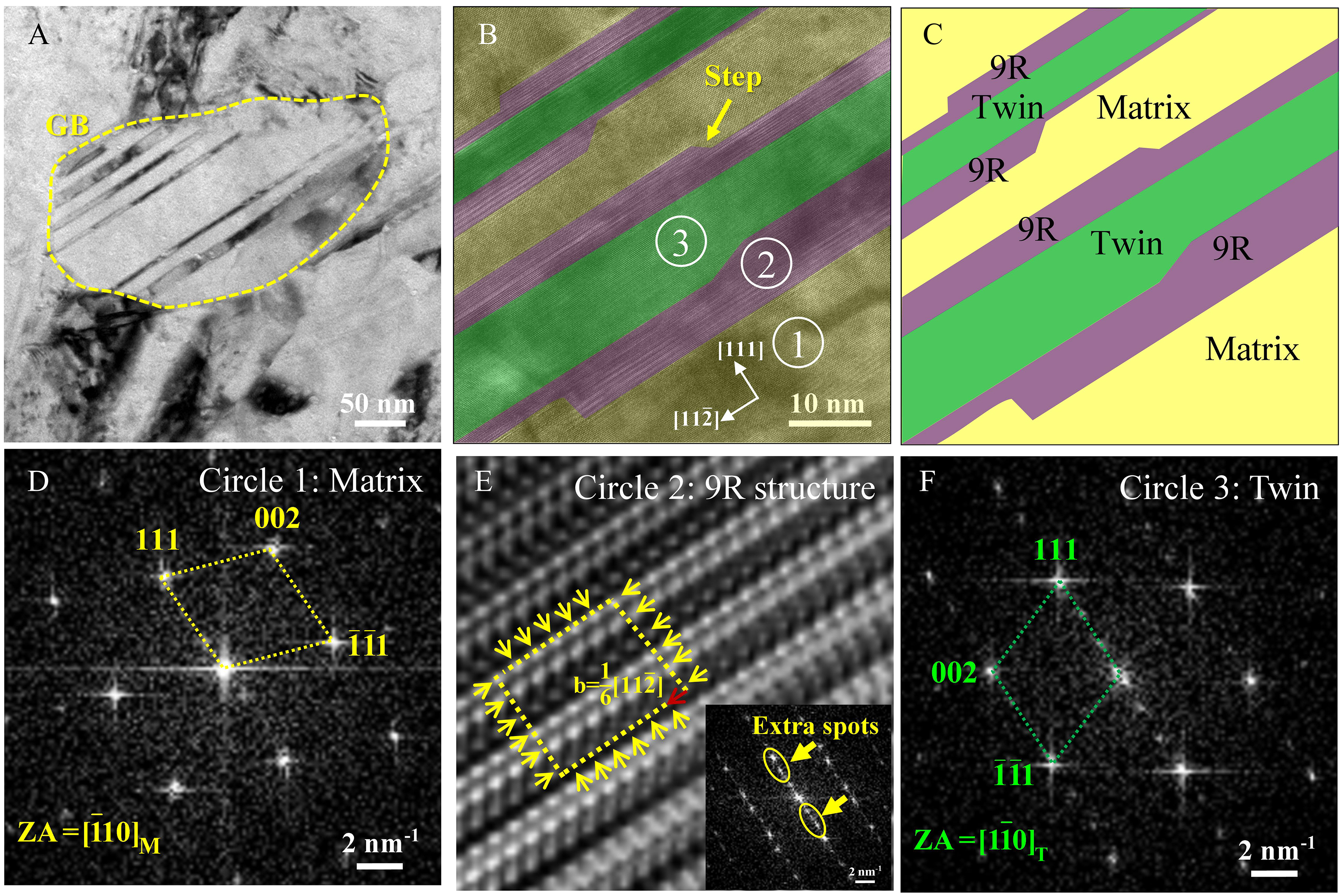
Figure 8. TEM results of twins fully extending through the grain: (A) BF image; (B) HRTEM image showing steps near the twins; (C) structural distribution map of (B); (D) FFT images of the region marked by white circle 1 in Figure 8B; (E) IFFT and FFT images of the region marked by white circle 2 in Figure 8B; (F) FFT image of the region marked by white circle 3 in Figure 8B. BF: Bright field; HRTEM: high-resolution transmission electron microscopy; FFT: fast Fourier transform; IFFT: inverse fast Fourier transform; GB: grain boundary; ZA: zone axis.


