


fig3
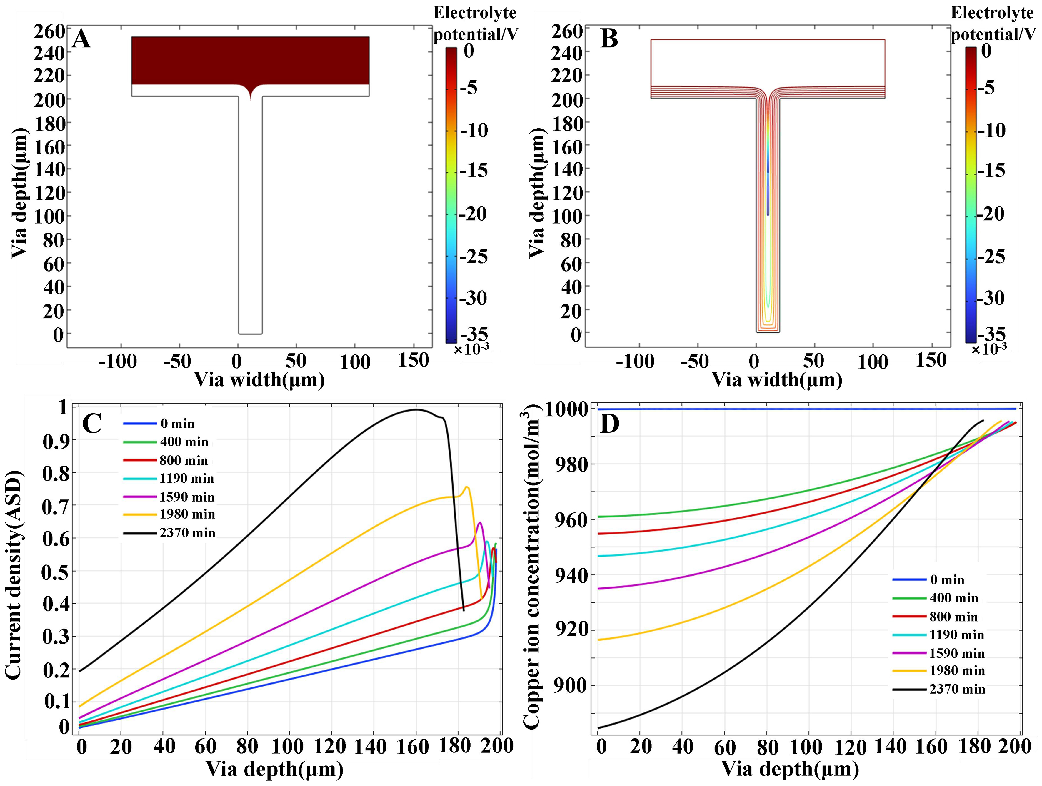
Figure 3. Simulation results of deep TSV electroplated copper at an additive concentration ratio of 1:10 and a current density of 0.15 ASD: (A) the electrolyte potential distribution after filling showing the defect-free filling result; (B) the electrolyte potential distribution at different electrodeposition times; (C) the current density distribution along the via depth at different electrodeposition times; (D) the distribution of copper ion concentration along the via depth at different electrodeposition times. TSV: Through silicon via; ASD: ampere per square decimeter.


