


fig11
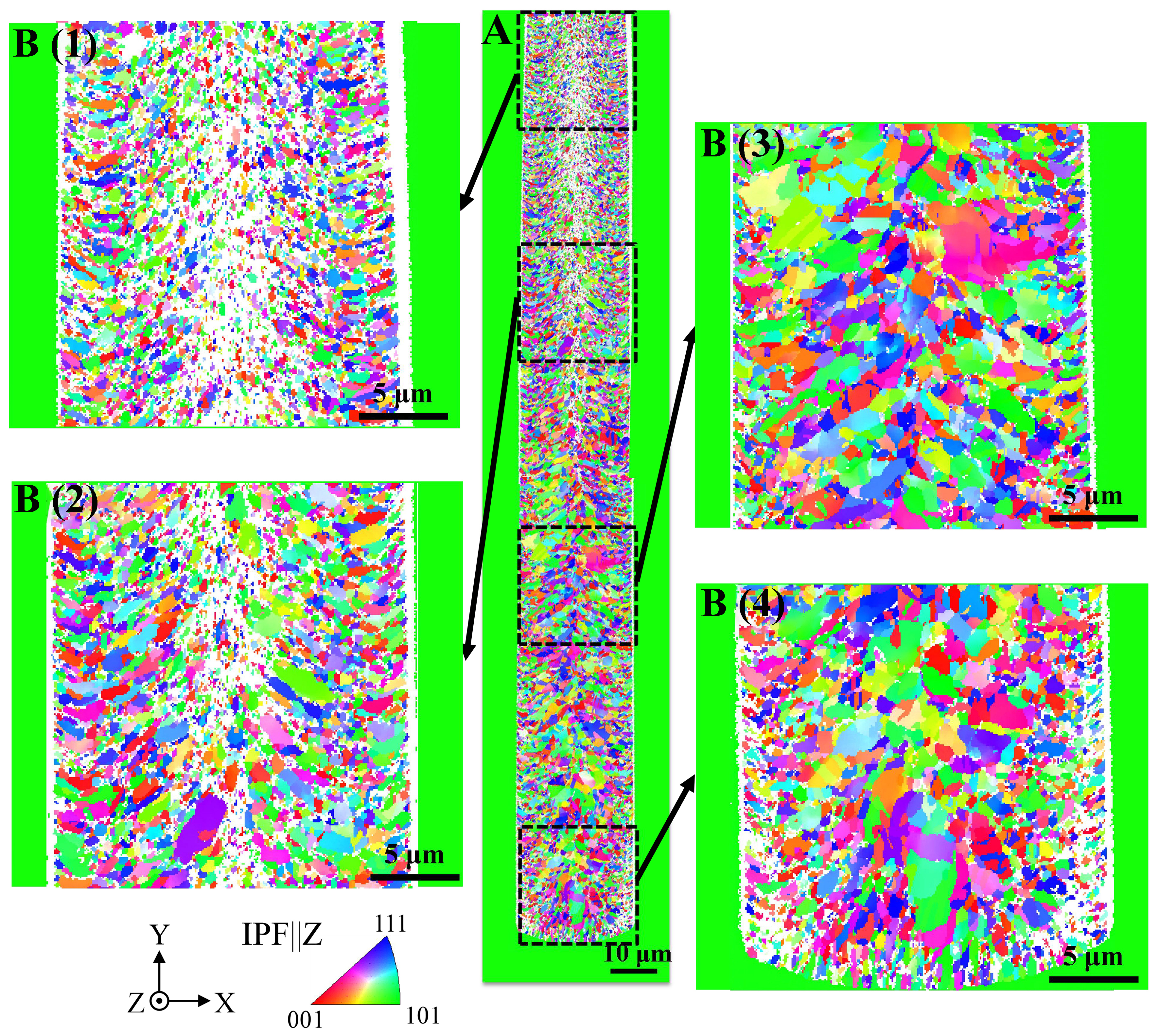
Figure 11. Microstructure and morphology of the deep TSV electroplated copper at a current density of 0.1 ASD and an additive concentration ratio of 1:10: (A) IPF||Z image; (B1-B4) local magnification of (A). TSV: Through silicon via; IPF: inverse pole figure; ASD: ampere per square decimeter.


