


fig6
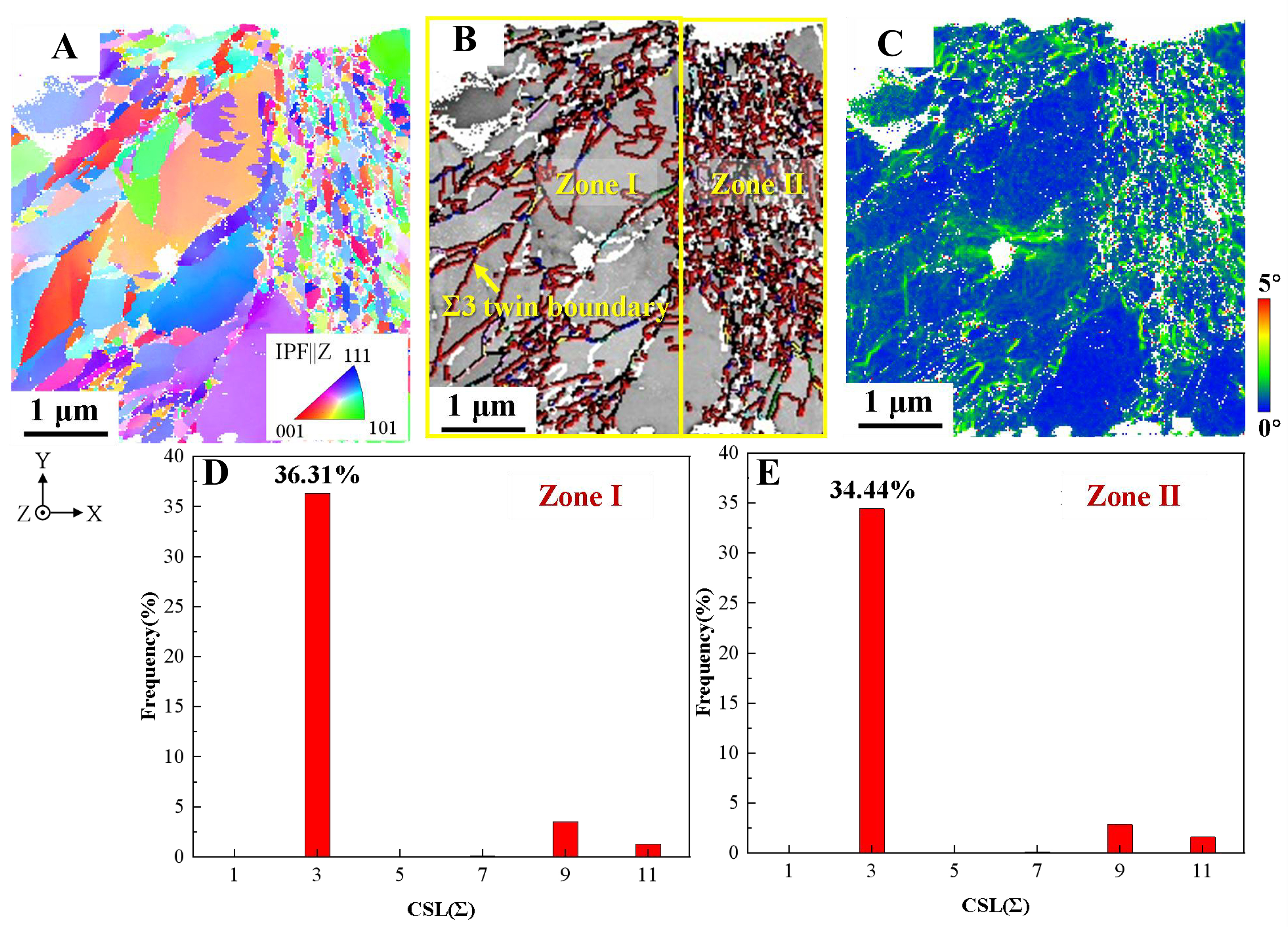
Figure 6. TKD results of region II in Figure 4A at a current density of 0.1 ASD and an additive concentration ratio of 1:10: (A) IPF||Z image; (B) band contrast and boundary distribution map; (C) KAM map;(D) twin boundary distribution of zone I in Figure 6B; (E) twin boundary distribution of zone II in Figure 6B. TKD: Transmission Kikuchi diffraction; IPF: inverse pole figure; KAM: kernel average misorientation; ASD: ampere per square decimeter.


