


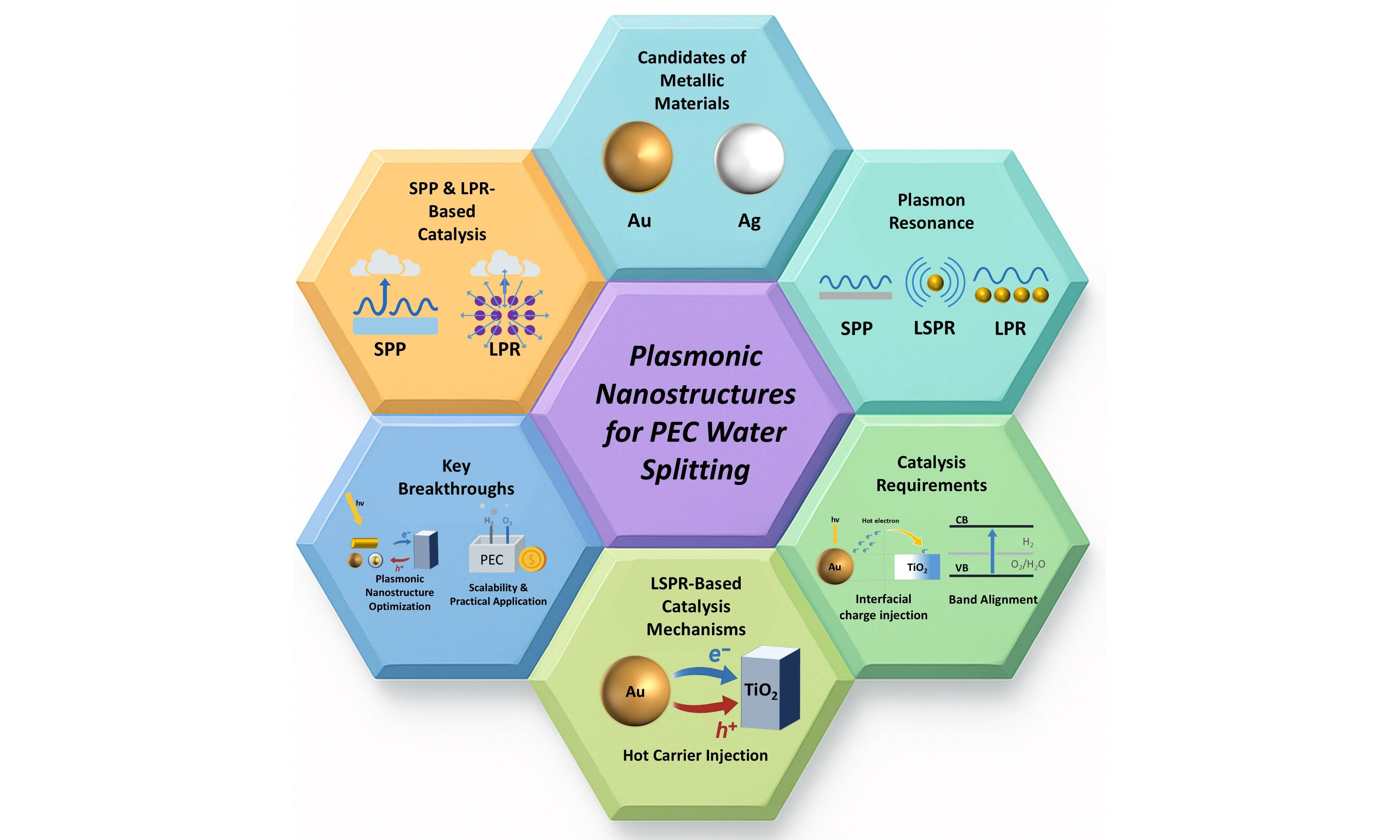
Photoelectrochemical water splitting from plasmonic nanostructures
 0
0 
Abstract
For sustainability, the development of new energy sources that do not produce carbon-based waste chemicals is crucial. Promising one is hydrogen, as combustion in atmospheric conditions only produces water. Currently, hydrogen production through water splitting has great potential. As there are many ways to perform it, solar-assisted electrocatalytic reaction could be one of the agenda items. Its ultimate goal is to efficiently perform the water-splitting process without external energy input, utilizing sunlight; however, its efficiency is a matter of controversy. From this perspective, the introduction of plasmonic materials is attractive, as there are many physical paths to maximize the efficiency of this process. To achieve this, a thorough understanding of plasmon resonance and the physical interactions between plasmons and semiconductors is required in advance. This review provides an in-depth look at these aspects, detailing methods for maximizing them, and not omitting the latest results. In this scope, we believe this review will be of great help to novices and experts in this field.
Keywords
INTRODUCTION
By reflecting on the environmental problems, the use of carbon-based fuels in energy production should be replaced with an environmentally friendly method. Next-generation fuel should be non-carbon dioxide-emissive, abundant, economically acceptable, and storable with high density. Amongst the candidates, hydrogen stands out as a promising option due to its exceptionally high gravimetric energy density (142 MJ/kg) known to date[1]. As solar energy is an unlimited energy source, potentially, photoelectrochemical (PEC) solar water splitting is ultimately able to produce hydrogen without external power. However, practical commercialization (approximately 2 USD/kg H2) has not been achieved yet[2].
To drive the water-splitting reaction, a minimum photovoltage of 1.23 V is required for the PEC solar water splitting application. Usually, oxide semiconductors, such as TiO2, Fe2O3, and BiVO4, are adopted. Due to the photoelectric effect, charge carriers (electrons and holes) are generated and transported to the surface to evoke the water-splitting reaction. They could absorb photons that have more energy than their bandgap. The theoretical maximum efficiency of PEC solar water splitting is foremostly governed by the bandgap of the electrode, as described by the Shockley-Queisser (SQ) limit[3,4].
In this context, approaches such as junction engineering, material composition modulation, doping, and photonic nanostructures have been extensively explored to match the absorption toward the AM 1.5G solar spectrum standard[5]. Among the various strategies, the introduction of plasmonic structures into the electrode has first emerged as a powerful option, as it offers an additional path of absorption of photons below their bandgap energy. Moreover, charge generation, charge transport, and interfacial charge transfer processes could be boosted with various mechanisms. These features indicate that additional activation of electrons in semiconductors via numerous mechanisms would lead to exceeding the classical SQ limit.
Herein, we present comprehensive guidelines for the recent developments of plasmon-enhanced PEC solar water splitting systems by reviewing the up-to-date approaches. Moreover, insights into performance enhancement are aimed at being provided. Specifically, this review focuses on how the integration of plasmonic nanostructures can improve photoelectrode performance regarding four critical aspects: light absorption, charge generation, charge transport, and interfacial electrochemical reactions. In addition to that, we provide future directions for improving the overall efficiency of plasmon-assisted PEC water splitting systems.
CATEGORIES OF PLASMONIC MATERIALS
To discuss the potential plasmonic materials toward solar water splitting applications, the inherent physical properties of the material, such as free electron density and permittivity, should be considered. To form a plasmonic excitation state, a vacant electronic state in a band (or nearby band) is required[6]. For the generation of plasmon resonance, photons should interact with electrons; through the process, the energy of the photon is dissipated. The excited free electrons are called ‘hot electrons’ and the non-excited free electrons are called ‘Drude electrons’[6]. The hot electrons (or holes) mainly determine the plasmonic property of materials.
Free-electron-based materials could fundamentally be able to be a plasmonic material [Figure 1A][7]. There are many candidates, such as conventional elemental metals (Al, Ag, Au, Cu, etc.), degenerated oxides (Indium Tin Oxide (ITO), Fluorine-doped Tin OXide (FTO), Aluminum-doped Zinc Oxide (AZO), etc.), and degenerated compounds (TiN, ZrN, etc.). Extraordinary, metal-insulator-transition (MIT) possible oxides also could possess plasmon resonance (e.g., VO2[8,9]). Especially, Ag and Au, so-called noble metals, have a great importance in the solar-to-fuel applications as they have localized surface plasmon resonance (LSPR) resonance in the VIS region. Full-width half-maximum (FWHM) values of wavelength
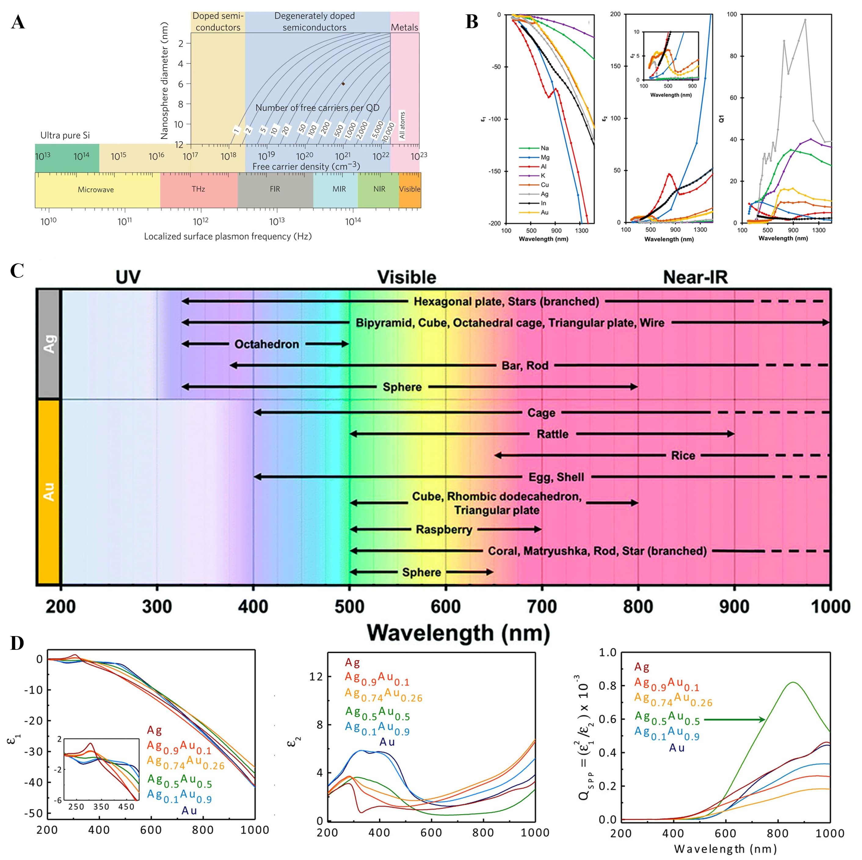
Figure 1. Considerations in the selection of plasmonic materials. (A) Localized surface plasmon resonance range of various materials[7]. Copyright 2019, published by Nature Publishing Group; (B) Dielectric functions of various plasmonic metals and calculated quality factors with resonant amplitude (Q1) and localized surface plasmon mode (Q2)[11]; (C) Shape dependence of plasmon resonance[11]. For (B and C), Copyright 2022, reproduced with CC-BY license. Published by the American Chemical Society; (D) Alloying with noble metal elements[20]. Copyright 2016, reproduced with permission. Published by the American Chemical Society. UV: Ultra-violet; FIR: far infra-red; MIR: middle infra-red; NIR: near infra-red.
Non-noble plasmonic metals (NNPM) could be an option [Figure 1B][11]. They are likely to show interband absorption in the ultraviolet visible (UV-VIS) region, but not restricted to[12]. As elements should have stability in environmental conditions, reactive alkali metals and alkali earth metals are hard to accept as a plasmonic component, though they possess high plasmon resonance quality factors[13]. Transition metals are representative NNPM materials, for further details, please refer to a recent prominent review[14].
Charge carrier density (nc) has linearity with bulk plasma frequency energy (ωp),
Due to the photothermal effect during plasmon excitation, thermally stable materials have a benefit in terms of stability. For example, ZrN and TiN have a bulk melting point over 2,500 °C[21]. Moreover, they have chemical stability in the harsh environment, which is good for plasmon-enhanced catalysis applications[22,23]. Nitride-based materials could possess a high-absorption efficiency from VIS to near infra-red (NIR) , which is promising for the goals of application[24]. Doped oxides could also be used as plasmonic materials. Light elemental doping, such as Li, Na, and H, could lead to the VIS to near-IR absorption. In that case, the amount of doping could be controlled with an external stimulus[25]. Heavy elemental doping, such as F, In, Sn, Ga, and vacancy oxygen, those materials tend to possess near-IR to far-IR absorption.
For the selection of plasmonic materials in solar-water splitting applications, absorption matching to the solar spectrum would be important. However, the electrolyte condition is rather harsh, thermal, chemical, electrochemical, and photo-stability is indispensable.
PLASMON RESONANCE
Fundamental description of plasmon resonance
Plasmons are collective oscillations of conduction electrons whose characteristics are determined by their spatial extent and coupling conditions[26]. In metals, bulk plasmons arise near the plasma frequency as longitudinal charge-density oscillations, whereas surface plasmons appear at metal-dielectric interfaces as lower-energy modes confined to the boundary[27]. When these surface modes couple to electromagnetic radiation at planar interfaces, they form surface plasmon polaritons (SPPs), which propagate along the interface while decaying evanescently into both the metal and the dielectric[28]. The dispersion relation of SPPs at a planar metal-dielectric interface can be obtained by solving Maxwell’s equations with appropriate electromagnetic boundary conditions and is given by the following equation[28,29]:
where k0 is the free-space wavevector. The imaginary component of kSSP determines the propagation length of SPPs along the interface[30], which defines the spatial range over which plasmonic energy can interact with the semiconductor depletion region. This spatial overlap critically governs whether non-thermal carriers generated during plasmon decay can be separated by built-in electric fields before thermalization[31]. Because direct phase matching between free-space photons and SPPs is prohibited by momentum mismatch, excitation typically relies on prism-based coupling schemes[28] or periodic grating structures[32]. In periodic architecture, reciprocal lattice vectors compensate for the momentum mismatch and enable resonant coupling through hybridization between diffractive orders and surface-bound modes, thereby extending the effective interaction length between optical fields and semiconductor charge carriers[32].
In contrast to propagating SPPs, LSPRs arise from the quantum confinement of conduction electrons within subwavelength metallic nanostructures[33]. Under the quasi-static limit, LSPR excitation concentrates electromagnetic energy into nanoscale volumes, generating intense near fields that decay within approximately 10 ~ 20 nm from the metal surface[34]. Consequently, effective photoelectrochemical enhancement requires that the photoactive semiconductor region be positioned within this near-field zone[35]. In the quasi-static limit, the resonance condition of dipolar localized surface plasmons is governed by the Fröhlich criterion derived from the dipolar term of Mie theory and is given by the following equation[33,36]:
which highlights the central role of the metal dielectric function and the surrounding environment in determining resonance energies. Notably, the Fröhlich condition can also be satisfied in heavily doped or defect-engineered metal oxides, where increased free-carrier densities and Fermi-level shifts induce a Drude-like dielectric response, thereby enabling LSPR beyond noble metals[37,38].
Collective plasmonic modes in periodic nanoparticle arrays bridge propagating and localized resonances through lattice-mediated coupling. Near diffraction conditions, hybridization between dipolar LSPR modes and in-plane diffractive orders form surface-lattice resonances (SLRs), which exhibit reduced radiative damping and enhanced spatial coherence across the array[39,40]. For photoelectrochemical applications, such collective modes enable spectrally selective enhancement when resonance conditions coincide with semiconductor absorption and carrier-collection probability under near-normal illumination[41]. However, because solar-driven systems benefit from broadband absorption, lattice-coupled resonances are most effective when integrated with broadband absorbers or multiplexed architectures that balance spectral selectivity with overall photocurrent generation[42].
Taken together, propagating SPPs, localized LSPRs, and lattice-coupled collective modes provide complementary pathways for manipulating light absorption, carrier generation, and interfacial charge transfer across distinct spatial and temporal scales[31,35,41]. By selecting and integrating these plasmonic modes according to device geometry, junction energetics, and material loss characteristics, plasmonic architectures can be rationally designed to address the key bottlenecks of photoelectrochemical water splitting[43].
Plasmon relaxation process
When metal nanostructures are excited by light, plasmons store energy as collective electron oscillations. This energy relaxes via two pathways on different time scales: (i) far-field photon emission and (ii) dissipation into electronic and lattice degrees of freedom. These pathways connect near-field concentration [Figure 2A] to hot-carrier generation and, ultimately, to thermal relaxation [Figure 2B-D][44,45].
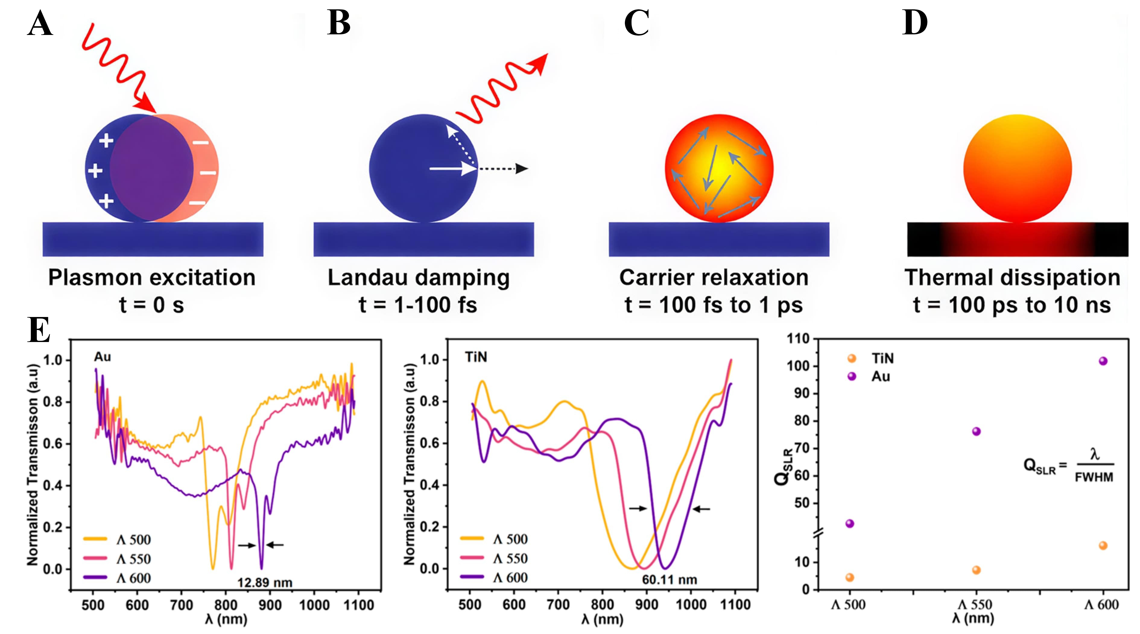
Figure 2. Ultrafast plasmon dynamics and lattice-controlled resonances. (A) LSPR excitation redirects the Poynting flux into the nanoparticle, resulting in near-field enhancement[45]; Copyright 2015, reproduced with permission. Published by the American Chemical Society. (B) Within 1 to 100 fs, Landau damping converts the plasmon into electron-hole excitations and permits radiative re-emission; this stage corresponds to a highly non-thermal carrier population (τnth)[45]. Copyright 2015, reproduced with permission. Published by American Chemical Society; (C) Over ~ 100 fs to 1 ps, electron-electron scattering drives energy redistribution toward a quasi-thermal distribution (τel)[45]. Copyright 2015, reproduced with permission. Published by the American Chemical Society; (D) From ~ 100 ps to 10 ns, phonon-mediated heat flow dissipates energy to the surroundings (τph)[45]. Copyright 2015, reproduced with permission. Published by the American Chemical Society; (E) Normalized transmission spectra of Au and TiN nanodisk arrays for lattice periods Λ = 500 to 600 nm (arrows indicate the FWHM at Λ = 600 nm) alongside the calculated surface-lattice-resonance quality factors QSLR=λ/FWHM[54]. Copyright 2025, reproduced with permission. Published by the Multidisciplinary Digital Publishing Institute. SLR: Surface-lattice resonance; FWHM: full-width half-maximum; LSPR: localized surface plasmon resonance.
Accordingly, the total plasmon damping rate can be expressed as the sum of radiative and non-radiative contributions[46,47]:
The spectral linewidth is quantified by the FWHM, γ, which is inversely related to the dephasing time T = 2ℏ/γ[46].
The radiative quantum efficiency is defined as the ratio of radiative to total damping rates[47]
For lattice-coupled nanoparticle arrays, the quality factor of SLR is commonly defined as[40]:
Particle shape and the optical environment determine the Γrad-Γnrad partition, thereby fixing γ and T[47]. Immediately after excitation, the carrier population is strongly non-thermal (τnth < 100 fs) owing to Landau damping, while subsequent electron-electron scattering (10-13 ~ 10-12 s, τel) drives rapid redistribution toward a quasi-thermal state - processes summarized in [Figure 2B and C][48]. Size- and surface-induced losses can be approximated as[49]:
where vF is the Fermi velocity, Leff is the effective mean free path set by particle size/roughness, and A is a geometry-dependent constant[49].
Hot-carrier collection and injection at the metal/semiconductor interface are governed by distance and energy. Defining the ballistic length lb≡vFτe-e, carriers can arrive before thermalization if the metal-semiconductor separation satisfies d < lb[48]. Injection further requires the energy condition E - EF ≥ ΦB - qΔV, where ΦB is the Schottky barrier and ΔV is the interfacial band bending under illumination or bias[50]. In practice, a moderate QSLR is targeted: an excessively large QSLR over-suppresses Γrad, whereas a moderate value preserves sufficient radiative coupling while Leff, d, and ΦB are co-tuned so that injection occurs within the τnth, τel time window[40].
During thermal relaxation (τph ≈ 10-10 ~ 10-8 s), electron-phonon coupling equilibrates the electron and lattice temperatures, followed by interfacial conductance and diffusion that remove heat to the surroundings - see [Figure 2D][51]. At this stage, the energy manifests primarily as photothermal effects that modulate the interfacial microenvironment but no longer contribute directly to hot-carrier injection.
The radiative pathway can be engineered via lattice coupling of localized plasmons. Near the Rayleigh anomaly, hybridization between dipolar LSPRs and in-plane diffractive orders forms subradiant SLRs [Figure 2E][40]. Maximizing QSLR requires λ ≈ λRA in a nearly symmetric refractive-index environment, whereas hot-carrier injection favors an intermediate QSLR that preserves radiative coupling while satisfying d < lb and E - EF ≥ ΦB - qΔV[40]. However, material losses ultimately limit performance: Au supports narrower linewidths and larger QSLR in the red/near-IR due to its smaller imaginary permittivity, whereas TiN exhibits higher non-radiative losses and broader linewidths even under lattice coupling [Figure 2E][52-54]. Moreover, chemical-interface damping introduces additional structure-dependent losses, emphasizing the need for surface-chemistry control during fabrication[55].
Plasmon-induced carrier transitions
When plasmons decay, energy is distributed between radiative emission and electronic excitations. Within the latter, intraband processes dominate at longer wavelengths, whereas interband d → sp transitions become increasingly prominent at shorter wavelengths[56]. Interband transitions arise from d → sp excitations whose energetic depth is governed by the proximity of the d band to the Fermi level, leading to deeper hole generation in noble metals [Figure 3A][52,57].
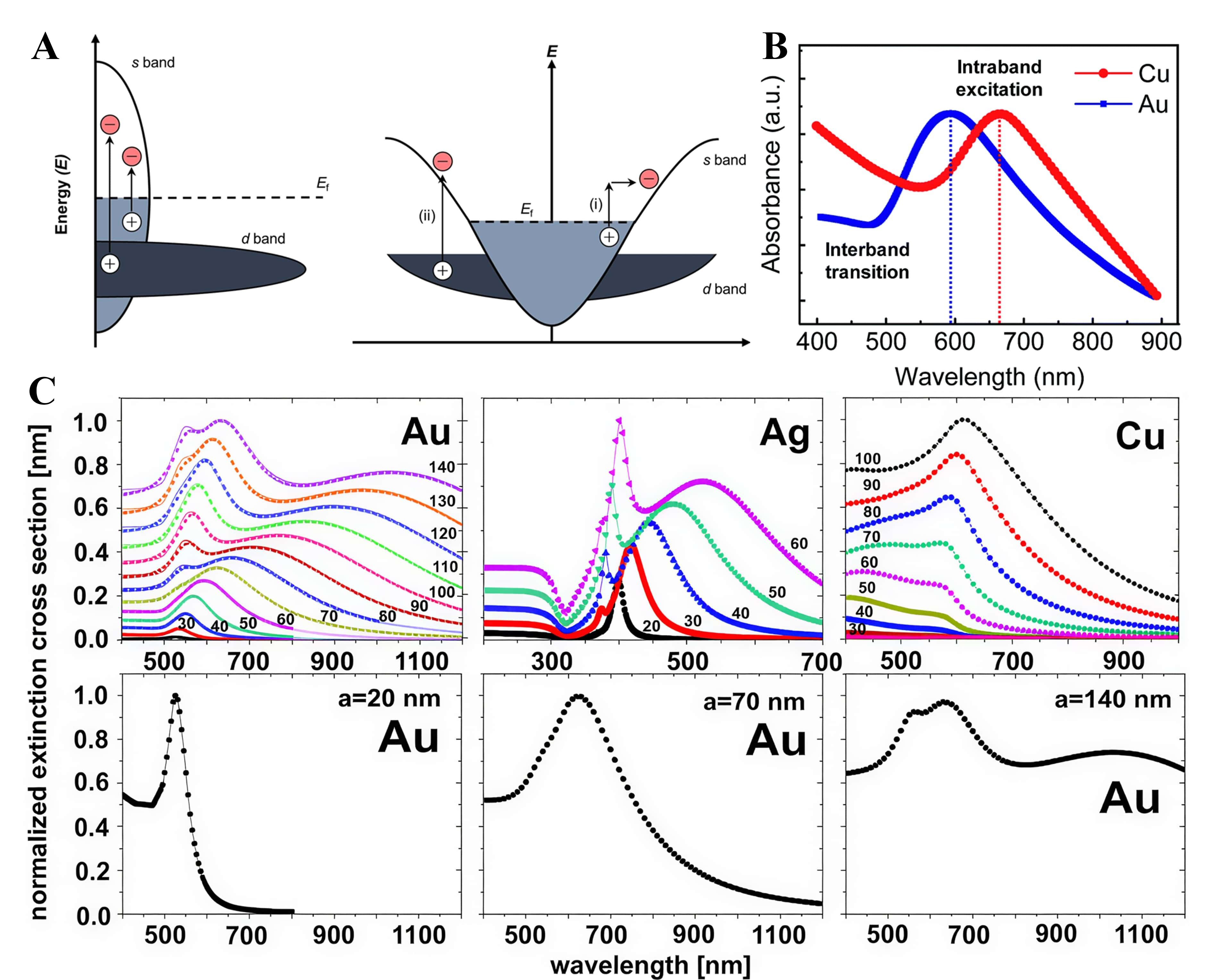
Figure 3. Electronic structure and plasmonic responses relevant to interband/intraband transitions. (A) Density-of-states schematic of a plasmonic (noble) metal and the corresponding E-k band diagram highlighting (i) intraband s → s acceleration and (ii) interband d → s transitions relative to EF[57]. Copyright 2018, reproduced with permission. Published by Wiley-VCH; (B) Absorbance spectra of plasmonic Cu and Au nanoparticles[60]. Copyright 2019, reproduced with permission. Published by the Royal Society of Chemistry. (C) Extinction spectra calculated for Au, Ag, and Cu nanospheres in water using COMSOL (points) and compared with Mie-theory results (solid lines) (upper). Extinction spectra highlighting multipole contributions (lower)[63]. Copyright 2016, reproduced with permission. Published by the Institute of Physics, Polish Academy of Sciences.
Particle size and modal content further regulate the intraband-interband balance. As shown in Figure 3C, ~20 nm Au spheres present a narrow dipolar peak (FWHM ≈ 80 nm) and primarily supply intraband electrons[62,63]. Increasing the radius to ~ 50-90 nm broadens the linewidth to ~ 180 nm, allowing the interband shoulder to merge with the plasmonic mode; this enables concurrent electron-hole generation and increases the extractable carrier flux[64]. At radii ≥ 140 nm, higher-order modes and strong scattering emerge; a sparse array of large particles then functions as a light-trapping antenna, extending the internal optical path in ~ 1 µm TiO2 films[65].
Synthesizing these primary reports yields a working picture for plasmonic photoelectrodes: intraband electrons tend to favor H2 evolution, whereas interband holes facilitate O2 evolution; their relative contributions are tunable via wavelength (material selection), particle size/shape, and junction design
Overall, this section establishes the fundamental plasmonic modes, relaxation pathways, and carrier-transition mechanisms that govern how optical energy is converted into extractable charge carriers, thereby providing the physical basis for the plasmon-enhanced photoelectrochemical processes discussed in subsequent sections.
FACTORS ON PLASMON-ENHANCED PHOTOELECTROCHEMICAL WATER SPLITTING
Requirements
Plasmonic enhancement in PEC photoelectrodes arises when incident photons efficiently couple into LSPR/SPP modes that localize electromagnetic fields at the reactive metal/semiconductor-electrolyte interface, and when interfacial charge transfer outpaces competing relaxation pathways[67]. Periodic lattices and particle arrays could compensate the photon-SPP momentum mismatch. By compensating energy at the junction, these structures maximize the local optical density of states at the interface. For example, hematite nanorods integrated with an Au nanohole array show order-of-magnitude increases in photocurrent and incident photon-to-current efficiency (IPCE) when an SPP-excited waveguide mode overlaps the absorption band[68]. Ultrafast spectroscopy on Au/TiO2 nanostructures indicates ≤ 50-fs electron transfer with high initial yields, establishing that plasmon decay can directly populate the semiconductor conduction band under resonant excitation[38]. Field-confining antenna-spacer-mirror cavities[69], gap-plasmon broadband absorbers[70], and grating-mediated coupling to 2D semiconductors[71] further amplify light absorption and raise hot-carrier photocurrents by factors of approximately two to ten, underscoring geometry as a primary lever for interfacial transfer without invoking non-plasmonic catalysts. In practice, design and diagnosis proceed in tandem, and optical modes are carefully engineered.
Chemical and electrochemical stability is essential for practical plasmon-enhanced PEC operation[72]. Under photoelectrochemical conditions, plasmonic metals would suffer corrosion (dissolution and/or surface oxidation), which can be assessed using Pourbaix-diagram-based potential-pH stability windows[73]. Overlap of PEC operating potentials with corrosion or dissolution regions induces nanostructure evolution and degrades long-term PEC performance[74].
Chemical interface damping
Chemical Interface Damping (CID) is a phenomenon in which the plasmon damping rate changes when several interfacial processes, such as molecular adsorption, charge transfer, electronic coupling with substrates, and defect states, act simultaneously or in combination at the metal interface[75].
The extent of CID rises as the adsorbate dipole moment grows; single-particle spectroscopy has demonstrated that adsorption of longer-chain thiols such as 1-decanethiol induces a broader homogeneous LSPR linewidth in Au nanorods compared to shorter analogs such as 1-butanethiol, indicating that stronger interfacial dipoles enhance damping[76]. This occurs through direct charge transfer from the excited plasmonic metal to adsorbed molecules at the nanostructure surface, leading to increased plasmon linewidth broadening and energy dissipation[77].
LSPR linewidth broadening can be represented as Γtot = Γbulk + Γrad + Γsurf + ΓCID. Bulk damping (Γbulk), radiation damping (Γrad), electron-surface damping (Γsurf), and CID (ΓCID)[62]. Γbulk is damping from inside the metal, Γrad is radiation damping (plasmons convert to photons), Γsurf is surface damping (increases with smaller nanostructure size), and ΓCID is additional LSPR energy loss due to charge transfer or electron orbital coupling with molecules adsorbed on the metal nanostructure surface.
Thermal and light effects
Temperature variations affect the electronic and optical properties of plasmonic nanostructures, primarily through changes in the dielectric constant of the metal, electron-phonon interactions, and thermal expansion[78,79]. For instance, in Au thin films, the imaginary part of the dielectric function at 500 °C becomes nearly twice as large as that at room temperature, indicating increased optical losses and reduced plasmonic quality factors[80]. As a result, the FWHM broadens at a plasmon peak resonance.
According to the Drude-Lorentz model, the damping term (Γ) in the dielectric function increases with temperature due to more frequent inelastic electron-phonon collisions[80]. In one study, temperature-induced changes in plasmonic properties were experimentally analyzed using UV-VIS-NIR spectroscopy[81]. This analysis revealed shifts in resonance peaks and variations in intensity, indicating alterations in electron density and plasmonic behavior[82].
A subsequent temperature rise leads to a localized increase in the dielectric constant, resulting in a decrease in the resonance frequency[83]. Conversely, blue shifts may occur under specific conditions, precipitated by structural alterations that result in a reduction of the resonance wavelength. Electron-electron scattering has been demonstrated to dissipate energy by increasing the frequency of collisions between free electrons when irradiated with strong light. Electron-phonon coupling has been shown to accelerate energy dissipation due to an increase in lattice vibrations.
Under photoelectrochemical operating conditions, plasmonic nanostructures are continuously driven far from thermodynamic equilibrium[84]. In this context, Pourbaix-type frameworks are adopted as a thermodynamic mapping tool to capture illumination-induced electronic shifts together with localized photo-thermal effects[85]. Plasmonic excitation leads to local heating and redistribution of photoexcited carriers, which dynamically modulate the effective electrochemical potential of plasmonic metals and alter the operational stability window. Such photo-thermal perturbations enhance plasmon damping and resonance broadening, ultimately contributing to time-dependent PEC performance degradation[85,86]. In photoelectrochemical operation, light absorption and localized photothermal heating dynamically shift the effective electrochemical potential of plasmonic metals, thereby modifying the accessible stability window during operation.
LSPR ENHANCED CATALYSIS
The overall plasmon‐mediated mechanisms are summarized schematically in Figure 4, while the detailed physical origins, governing processes, and interfacial charge‐transfer pathways associated with each mechanism are discussed in the corresponding subsections.
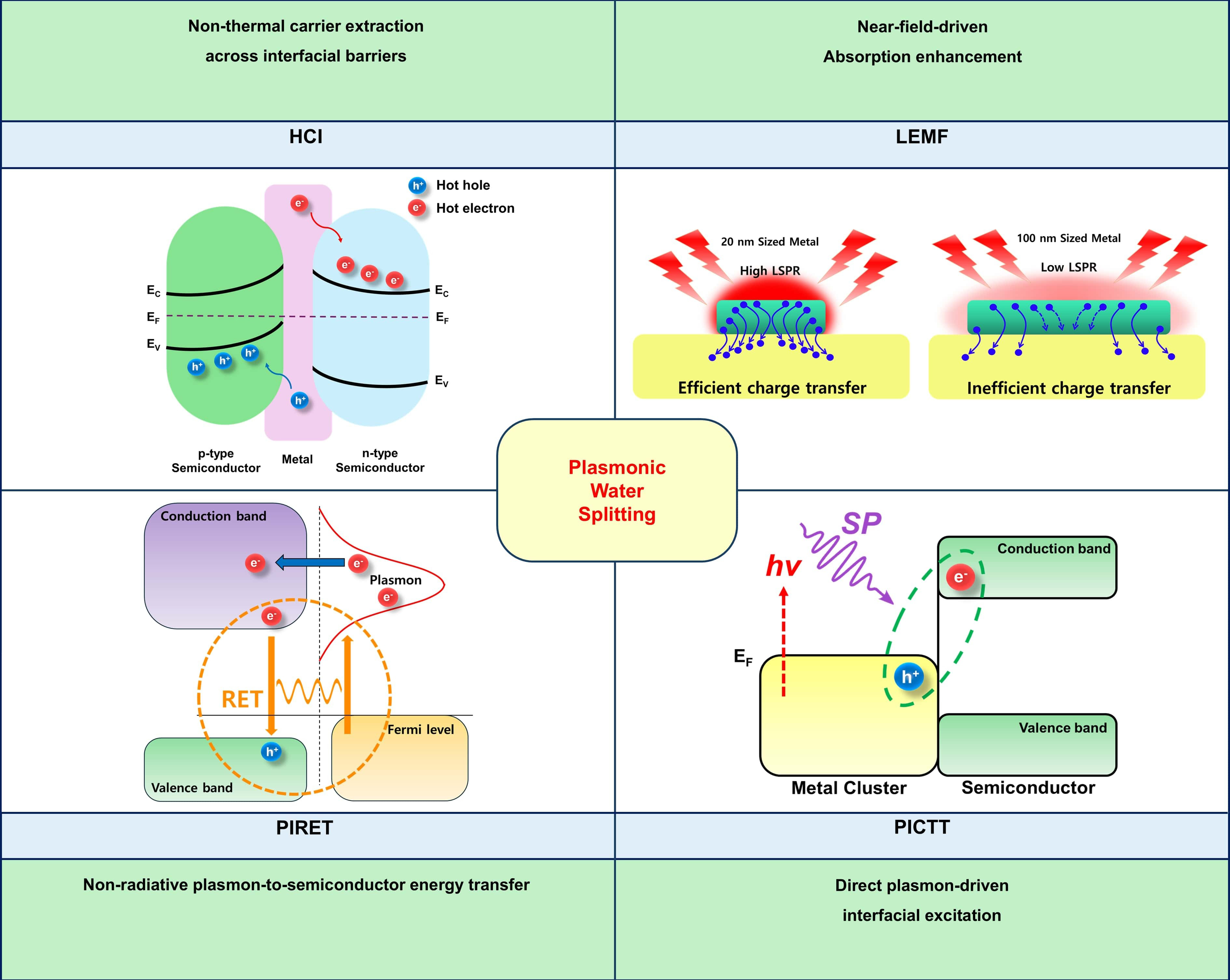
Figure 4. Schematic illustration of plasmonic mechanisms in photoelectrochemical water splitting. The upper left panel illustrates HCI, where non-thermal electrons and holes generated by plasmon decay traverse interfacial energy barriers[87]. Copyright 2025, reproduced with permission. Published by American Chemical Society. The upper right panel depicts LEMF, in which near-field concentration around plasmonic nanostructures amplifies optical absorption and charge generation in the adjacent semiconductor[144]. Copyright 2021, reproduced with permission. Published by American Chemical Society. The lower left panel shows PIRET, a non-radiative process that transfers plasmon energy to semiconductor excitations without direct carrier injection[123]. Copyright 2012, reproduced with permission. Published by American Chemical Society. The lower right panel represents PICTT, where plasmon excitation directly drives electronic transitions across the metal-semiconductor interface[88]. Copyright 2019, reproduced with permission. Published by American Chemical Society. HCI: Hot carrier injection; PIRET: plasmon-induced resonant energy transfer; LEMF: localized electromagnetic field enhancement; PICTT: plasmon-induced metal-to-semiconductor interfacial charge-transfer transition; LSPR: localized surface plasmon resonance; SP: surface plasmon; EC: conduction band edge; EF: Fermi Leve; EV: valance band edge.
Shockley-Queisser limit
While the SQ framework establishes the efficiency ceiling for single-junction solar conversion, photoelectrochemical water splitting is further limited by the thermodynamic requirement of the hydrogen evolution process[89,90]. Nonetheless, in the context of solar-driven water splitting, it is imperative to consider additional factors such as Faradaic efficiency[91]. Smaller bandgaps sustain excessive photocarrier thermalization losses, while larger bandgaps limit photon absorption and thus reduce photocurrent, leading to the characteristic peak at the intermediate bandgap and efficiency decline toward both ends of the spectrum [Figure 5A][92].
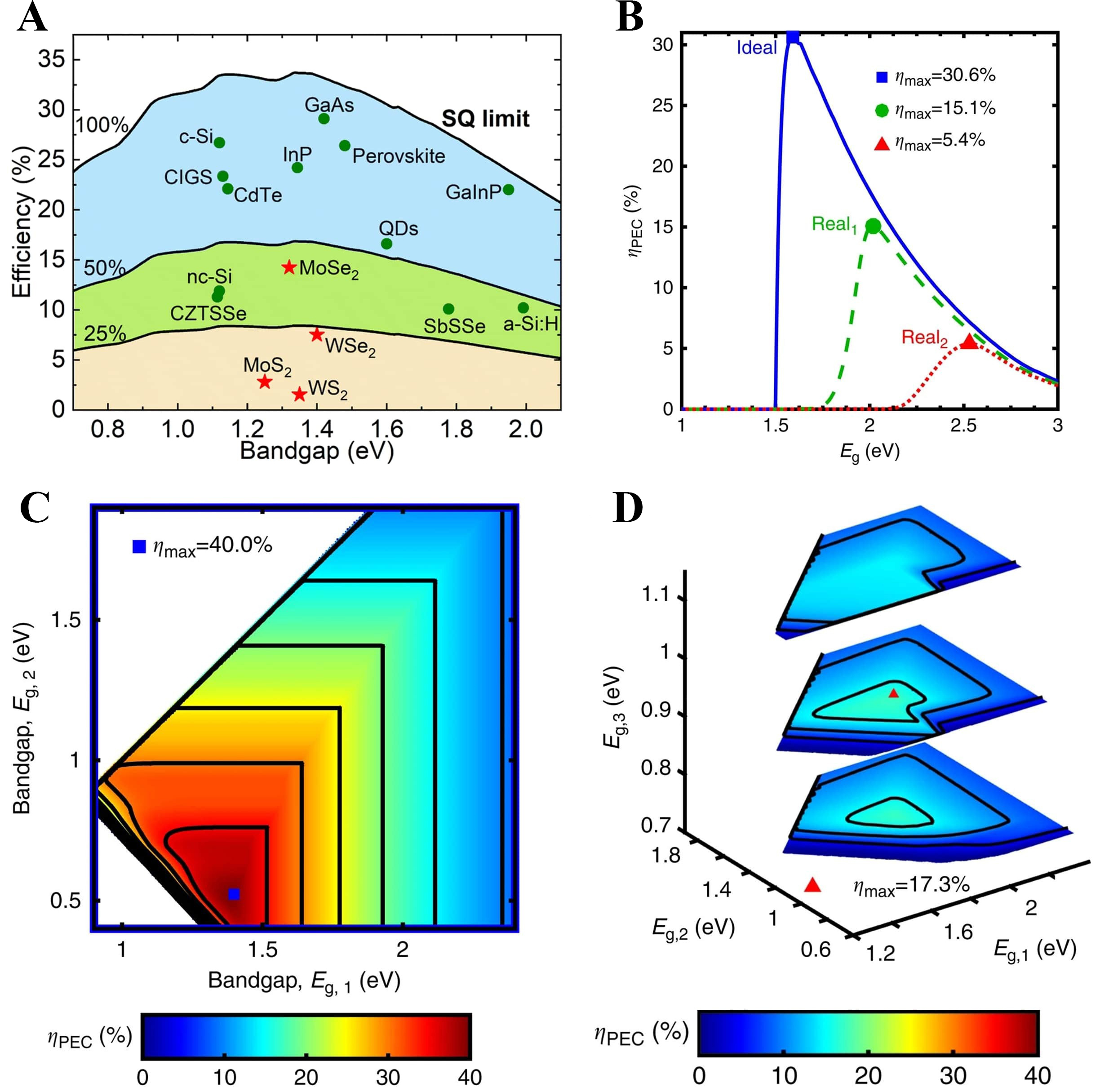
Figure 5. SQ-derived thermodynamic ceilings for solar-to-hydrogen conversion. (A) SQ limit and the bandgap-efficiency relation of various semiconductors[92]. Copyright 2023, published by the Royal Society of Chemistry; (B) The calculated single-junction PEC efficiencies are represented by the following colors: blue for ideal conditions, green for the best-in-class assumptions, and red for earth-abundant assumptions[94]; (C) The ideal dual-junction PEC efficiency map[94]; (D) The efficiency surface for the earth-abundant triple-junction case[94]. Copyright 2016, reproduced with permission. Published by Springer Nature. CZTSSe: Copper-zinc-tin sulphide/selenide quantum dot; QD: quantum dot; PEC: photoelectrochemical; ηPEC: photoelectrochemical water splitting efficiency; Eg: bandgap energy; SQ: Shockley-Queisser.
Due to overpotential constraints, PEC efficiency emerges only within a limited bandgap window and declines outside this range, whereas dual and multi-junction designs mitigate these limitations through bandgap balancing across junctions [Figure 5B-D][93,94]. The incorporation of Au nanoparticles, which exhibit LSPR, enables unique charge generation and energy transfer processes that extend beyond conventional photovoltaic mechanisms[95].
Plasmonic photoelectrochemical systems enhance light utilization and carrier dynamics through non-equilibrium processes that are not captured by conventional photovoltaic models[96]. In this context, the SQ limit defines the thermodynamic benchmark for equilibrium-based solar conversion and is employed here as a reference framework for interpreting how plasmon-mediated effects, discussed in the following sections, extend the fundamental limits of water-splitting photoelectrodes.
Hot carrier injection and IPCE enhancement
LSPR-excited metal nanoparticles undergo two principal decay pathways [Figure 6A][97]. Hot-carrier generation is dominated by non-radiative plasmon decay, which directly converts plasmon energy into energetic charge carriers, whereas radiative decay primarily re-emits photons into the far field and contributes minimally to carrier injection[98,99]. As schematically illustrated in metal-semiconductor junctions, carriers with kinetic energies exceeding the Schottky barrier height can be injected into the semiconductor conduction band [Figure 6B][97].
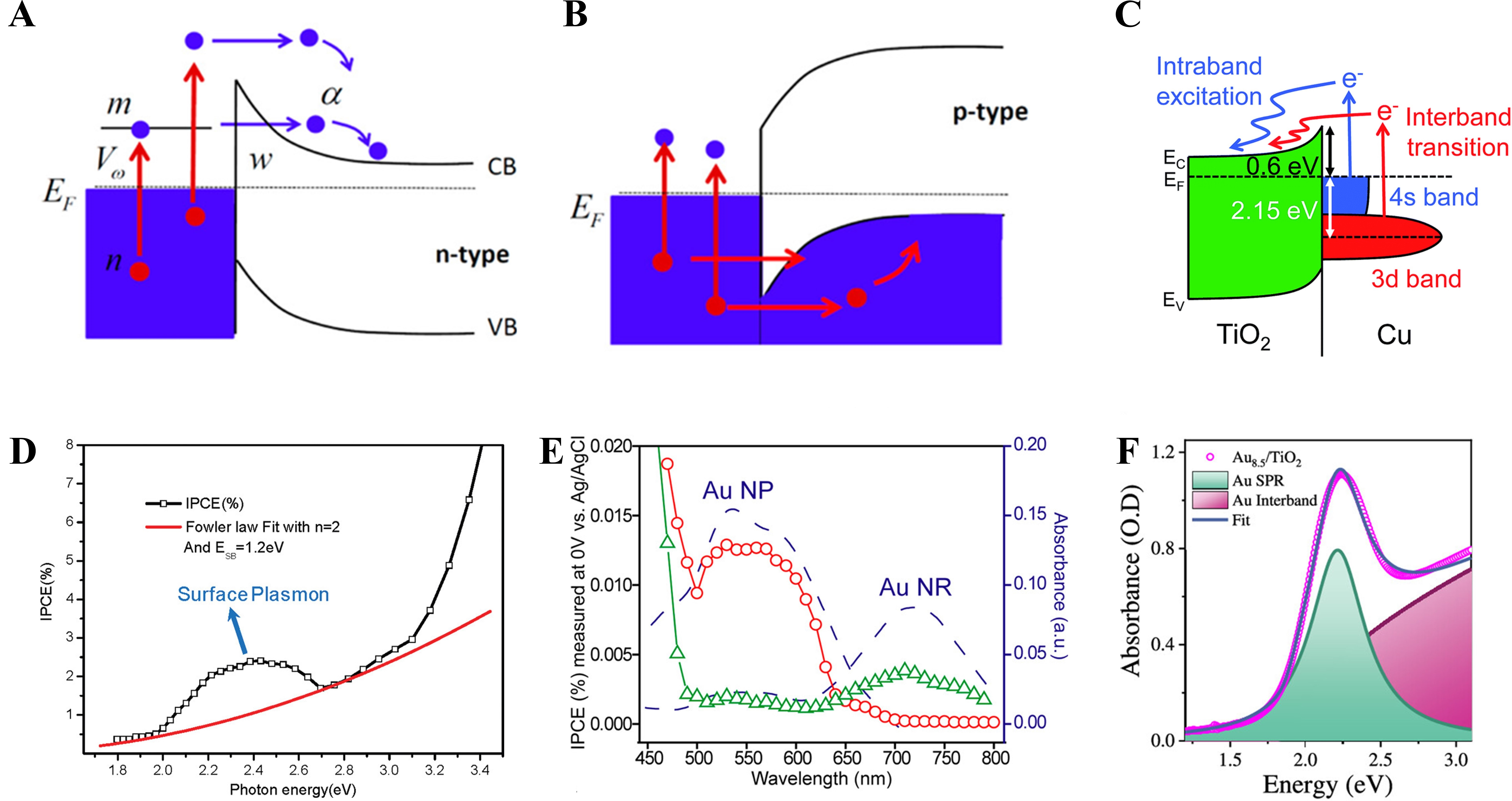
Figure 6. Mechanisms of Plasmon-Induced HCI and Resulting IPCE Enhancement in Metal-Semiconductor. (A) n-type semiconductor junction; (B) p-type semiconductor junction[97]. Copyright 2013, reproduced with permission. Published by the American Chemical Society; (C) Band alignment of Cu/TiO2, emphasizing band excitation processes[60]. Copyright 2019, published by the Royal Society of Chemistry; (D) IPCE-photon energy dependence with surface plasmon enhancement region and Fowler law fitting[105]. Copyright 2011, published by the American Chemical Society; (E) Wavelength-resolved IPCE and absorption spectra of Au nanoparticles and Au nanorods[106]. Copyright 2013 American Chemical Society; (F) Absorption spectrum decomposition of Au/TiO2 into LSPR and interband contributions[107]. Copyright 2025 American Chemical Society. CB: Conduction band; EC: conduction band edge; EF: Fermi Leve; EV: valance band edge; VB: valance band; IPCE: incident photon-to-current efficiency; NP: nano-particle; NR: nano-rod; LSPR: localized surface plasmon resonance.
The excitation pathways underlying hot-carrier generation are reflected in the IPCE spectra of Cu/TiO2 nanodiodes. Figure 6 illustrates the band alignment at the Cu/TiO2 junction, where intraband excitation produces a broad low-energy carrier distribution, while interband excitation corresponds to 3d to 4s electronic transitions in Cu, selectively enabling high-energy electrons to participate in interfacial charge transfer[60]. These distinct excitation channels extend light harvesting beyond the intrinsic bandgap of the semiconductor absorber, enabling additional carrier generation within the photoelectrode[100].
Hot-carrier injection (HCI) requires appropriate energetic alignment between the metal Fermi level and the semiconductor band edges, enabling hot electrons generated near the metal surface to overcome the Schottky barrier and inject into the conduction band of an n-type semiconductor such as TiO2[101]. Simultaneously, hot carriers originating from d-band to sp-band transitions can participate in oxidation reactions at the metal-electrolyte interface, thereby maintaining charge neutrality during interfacial transfer processes[102].
In plasmonic metal-semiconductor hybrids, enhancement of IPCE is therefore closely associated with efficient hot-carrier injections across the interfacial barrier[103,104]. The IPCE spectra of Cu/TiO2 nanodiodes display distinct band features, confirming contributions from both excitation pathways to photocurrent generation. Plasmon-assisted processes are identified by deviations from Fowler’s law in the IPCE-photon energy spectrum, which defines the energy window where surface plasmon effects dominate carrier generation [Figure 6D][105]. Comparisons between spherical and nanorod-decorated Au/TiO2 photoelectrodes further reveal that the longitudinal LSPR mode in nanorods extends the IPCE response toward longer wavelengths [Figure 6E][105,106]. Accordingly, combining different particle geometries enables broadband optical absorption, while reducing particle size enhances hot-electron injection efficiency [Figure 6F][107]. These observations indicate that charge generation and injection are optimized when the plasmon resonance is spectrally aligned with interband transition energies[108].
Under realistic operating conditions, IPCE serves as a primary metric for evaluating optical-to-electrical energy conversion efficiency in photoelectrochemical systems by capturing deviations from the idealized SQ framework arising from plasmon-mediated non-equilibrium carrier pathways[109]. Among these pathways, hot carrier injection directly converts plasmon decay into photocurrent by enabling energetic electrons to cross the metal-semiconductor barrier, thereby extending photoelectrochemical water splitting into sub-bandgap spectral regions and enhancing IPCE under visible light illumination.
Local electro-magnetic field-enhancement
In photoelectrochemical water splitting, Local Electro-Magnetic Field-enhancement (LEMF) intensifies light-matter interactions beyond the intrinsic absorption of semiconductor photoelectrodes[74]. Plasmonic nanostructures generate electromagnetic near-fields that increase the local photon density by several orders of magnitude within nanometer-scale regions adjacent to the semiconductor surface[110], thereby enhancing electron-hole pair excitation. Unlike macroscopic light-trapping strategies based on scattering or texturing, LEMF compresses electromagnetic energy into sub-wavelength volumes[43].
LEMF is defined as the resonant amplification of the optical near-field within a few nanometers of a plasmonic nano-object, producing nanometer-scale electromagnetic hot spots[111,112]. Importantly, LEMF redistributes electromagnetic energy without increasing the total incident light intensity. Finite-difference time-domain (FDTD) simulations show that closely spaced plasmonic nanoparticles, such as a linear five-sphere Au nanochain, generate pronounced near-field hot spots at interparticle gaps, resulting in stronger local electromagnetic fields and enhanced light absorption compared with isolated particles [Figure 7A][113,114].
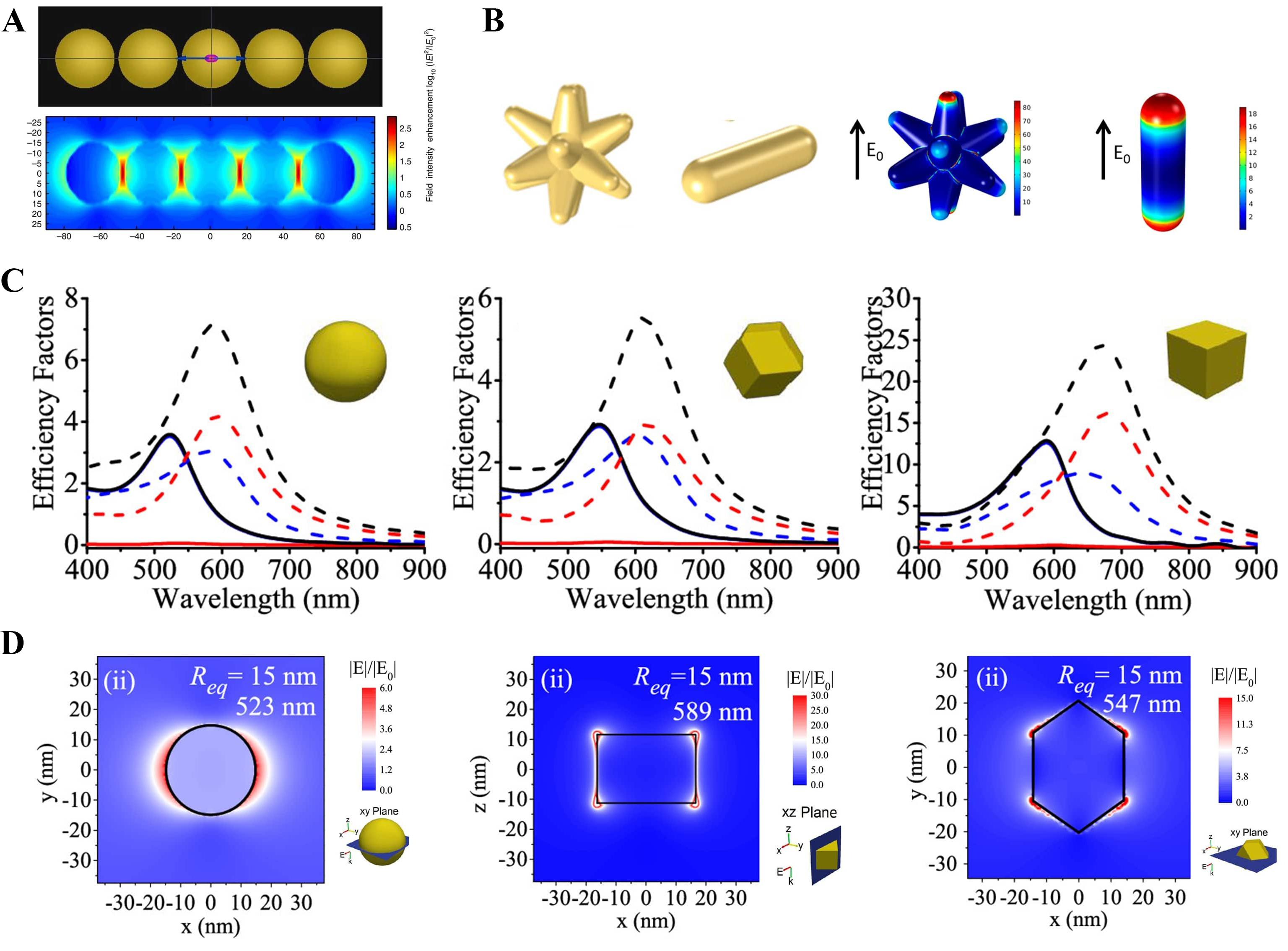
Figure 7. The shape- and coupling-dependent plasmonic responses of Au nanostructures are of particular interest. (A) FDTD map of a five-sphere chain showing longitudinal hotspots[114]. Copyright 2019, reproduced with permission. Published by John Wiley and Sons; (B) Field localization patterns of star- and rod-shaped Au antennas[115]. Copyright 2020, reproduced with permission. Published by the American Chemical Society; For (C and D) Extinction, scattering, and absorption efficiencies for nanoparticles with an equivalent radius of 15 nm, together with electric-field distributions at the primary LSPR modes highlighting edge and corner-localized hot-spots[120]. Copyright 2019, reproduced with permission. Published by the American Chemical Society. E0: Incident electric field; FDTD: finite-difference time-domain; Req: equivalent radius; LSPR: localized surface plasmon resonance.
The amplification of the electric field by LEMF is contingent upon the geometry, gap, and material composition of the nanostructure. Comparison of star- and rod-shaped Au antennas shows that sharp, tip-dominated morphologies strongly enhance LEMF through the lightning-rod effect, while simultaneously enabling tunable longitudinal LSPR modes extending into the near-infrared, consistent with experimentally observed field enhancement in nanostar geometries. This localized field amplification increases the effective excitation rate of electron-hole pairs in the adjacent semiconductor, thereby enhancing carrier generation over a broader interfacial area compared to nanorods [Figure 7B][115].
This localized effect gives rise to spatially confined zones of enhanced photoactivity, which are sometimes referred to as plasmonic hot-spots[116]. In these regions, enhanced photon absorption and carrier generation reduce recombination losses by shortening carrier diffusion lengths, while the strong localized field can additionally modulate band bending within the semiconductor[117]. This, in turn, results in the modification of the built-in electric field that serves as the driving force for carrier separation. This modification has the potential to facilitate the extraction of holes to the electrolyte and enhance the efficiency of water oxidation kinetics[118].
Figure 7C and D together demonstrate that non-spherical Au nanoparticles exhibit enhanced optical efficiencies because their anisotropic geometries promote stronger localization of the electromagnetic near field. The efficiency factors in Figure 7C increase with shape anisotropy, while Figure 7D directly visualizes the corresponding enhancement of local field intensity, governed by geometry, dielectric environment, and coupling effects[119,120].
LEMF concentrates optical energy near the semiconductor interface, increasing carrier generation where electrochemical reactions occur. In photoelectrochemical water splitting, this near-field localization improves charge separation and reduces recombination losses without increasing incident light intensity.
Plasmon induced resonant energy transfer
Resonant energy transfer (RET) is a non-radiative process in which excitation energy migrates from a donor to an acceptor through dipole-dipole coupling[121]. Plasmon-induced resonance energy transfer (PIRET) is a non-radiative mechanism that transfers plasmonic excitation energy from metal nanoparticles to adjacent semiconductors through near-field dipole coupling, without direct electron transfer[122]. For instance, in Ag@TiO2 structures, the spectral overlap between the LSPR and the TiO2 absorption edge enables PIRET, while the direct metal-semiconductor contact simultaneously allows hot electron injection [Figure 8A][122].
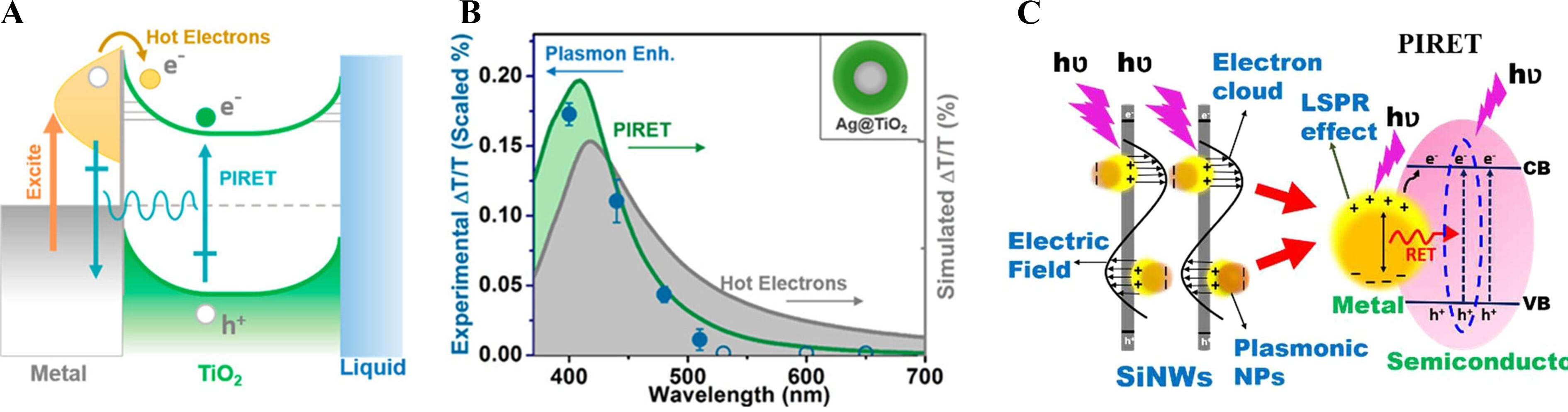
Figure 8. PIRET as a key mechanism for excitonic energy transfer in plasmonic systems. For (A and B) Schematic and spectral evidence of PIRET in Ag@TiO2, highlighting plasmon-mediated energy transfer distinct from hot-electron processes[122]. Copyright 2015, published by the American Chemical Society; (C) Conceptual diagram of PIRET from plasmonic nanoparticle to semiconductor[127]. Copyright 2024, published by the American Chemical Society. PIRET: Plasmon-induced resonance energy transfer; LSPR: localized surface plasmon resonance; CB: conduction band; VB: valance band; hν: energy of photon; NP: nano-particle.
To facilitate this interaction, an ultrathin spacer with a thickness of 1-3 nanometers is introduced, ensuring effective coupling without requiring a direct tunneling channel[123]. In the case of Ag@SiO2@TiO2, the insertion of a ~ 10 nm insulating SiO2 layer blocks hot electron injection, yet PIRET remains operative due to the preserved spectral overlap between the plasmon and the semiconductor [Figure 8B][122]. Under these conditions, a substantial increase in the local density of photogenerated electron-hole pairs has been reported within nanometer-scale volumes[124].
PIRET bypasses the Schottky barrier through resonant interfacial energy exchange, enabling ultrafast charge population and substantial enhancement of photoelectrochemical reaction rates without altering the open-circuit potential[124,125]. FDTD simulations further confirm that geometric sharpening and reduced interparticle gaps amplify near-field intensity, thereby increasing PIRET efficiency without changing overall device absorbance[126]. Figure 8C provides an integrated conceptual view, illustrating that plasmonic nanoparticles can simultaneously mediate resonant energy transfer, carrier injection, and radiative processes[127].
PIRET enables non-radiative energy transfer from plasmonic metals to semiconductors through near-field coupling, bypassing interfacial charge-injection barriers. This mechanism enhances exciton generation near the interface while preserving the electrochemical potential required for water-splitting reactions.
Plasmon-induced interfacial charge transfer transition
Plasmon-induced interfacial charge transfer transition (PICTT) is a distinct pathway in which plasmon decay directly excites electrons from a metal into an adjacent semiconductor, enabling instantaneous interfacial charge separation while bypassing multistep loss channels[128]. This contrast to plasmon-induced hot electron transfer (PHET) is schematically illustrated at an Ag/TiO2 junction [Figure 9A][129].
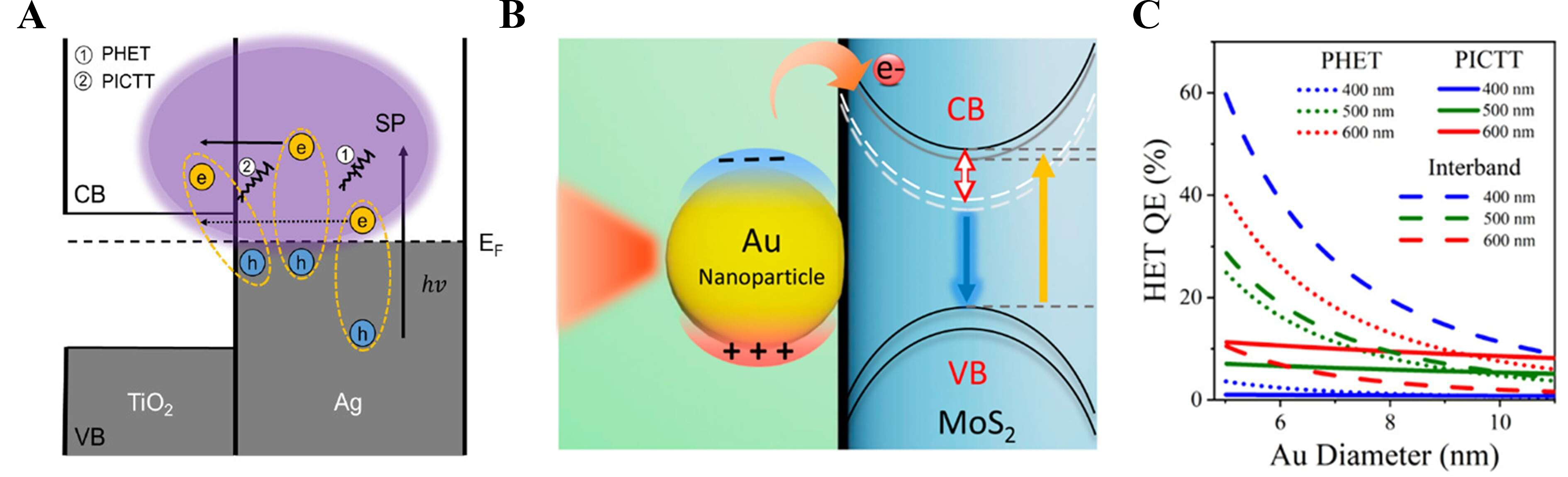
Figure 9. Effects of PICTT on interfacial charge transfer and plasmonic activity. (A) Energy diagram contrasting PHET and PICTT across an Ag/TiO2 junction[129]. Copyright 2021, reproduced with permission. Published by the American Chemical Society; (B) Au-nanoparticle-induced charge separation and exciton dissociation at an Au/MoS2 interface[132]. Copyright 2015, published by the American Chemical Society; (C) Exciton peak shift versus 532 nm laser power, tracking plasmonic doping[107]. Copyright 2025, published by the American Chemical Society. PHET: Plasmon-induced hot electron transfer; PICTT: plasmon-induced interfacial charge transfer transition; SP: surface plasmon; CB: conduction band; VB: valance band; EF: Fermi Leve; HET: hot electron transfer; QE: quantum efficiency; hν: energy of photon.
The concept of PICTT was first supported by ab-initio simulation studies. Long and Prezhdo employed time-domain density functional theory with nonadiabatic molecular dynamics to show that upon plasmon excitation in an Au-TiO2 system, an electron can be injected into the TiO2 conduction band almost instantaneously[130]. Crucially, this occurs without requiring the intermediate formation and thermalization of carriers in the metal nanoparticle[131]. A representative experimental manifestation is shown in Figure 9B, where Au nanoparticles induce efficient charge separation and exciton dissociation at the Au/MoS2 interface, evidencing interfacial charge-transfer transitions in strongly coupled heterostructures[132].
Building on this theoretical prediction, subsequent experimental work provided direct evidence for plasmon-induced metal-to-semiconductor interfacial charge transfer transitions and formally established the concept of PICTT[130]. They studied CdSe semiconductor nanorods decorated with Au tips, a strongly coupled metal-semiconductor heterostructure, and observed highly efficient plasmon-induced electron injection from the Au into the CdSe[133]. Interfacial charge transfer from Au plasmons into CdSe strongly damps the plasmon resonance and generates a substantial electron population in the semiconductor. The polarization dependence of this yield indicates that the orientation of plasmon oscillation relative to the interface governs the transfer process[134].
Size and wavelength-dependent competition between PICTT and hot-electron-mediated pathways is quantitatively illustrated by the PHET quantum efficiency map, which shows that PICTT dominates for smaller Au nanoparticles and shorter excitation wavelengths, whereas hot-electron transfer becomes increasingly significant for larger particle diameters and longer wavelengths [Figure 9C][107].
Within plasmonic photoelectrochemical water splitting, PICTT directly couples plasmon decay to instantaneous interfacial charge separation, thereby bypassing thermalization losses associated with hot-carrier-mediated pathways. Through this direct charge-transfer channel, plasmonic nanostructures actively participate in driving water oxidation and reduction reactions rather than functioning solely as optical enhancers.
Quantum tunneling injection
Quantum tunneling injection (QTI) arises when plasmon-generated hot electrons penetrate an ultrathin Schottky barrier via wavefunction tunneling, enabled by the non-thermal carrier population produced through Landau damping during LSPR decay[135,136]. Compared with carriers generated by direct band excitation, plasmon-induced electrons exhibit broader energy distributions and enhanced out-of-plane momentum components, which favor barrier penetration and render QTI particularly effective in strongly confined Au or Ag nanostructures below 10 nm[137,138]. The tunneling probability is further governed by interfacial engineering, as depletion-width compression through interfacial states, strain, doping, and dipole modulation enables sub-nanometer barrier profiles in metal-semiconductor heterojunctions[139,140]. By extracting hot carriers before thermalization, quantum tunneling injections enable sub-bandgap photon utilization and directly enhance the IPCE and visible-light photocurrent of plasmon-modified TiO2 photoelectrodes[108,141-144].
SPP AND LATTICE PLASMON RESONANCE ENHANCED CATALYSIS
Scattering enhancement
The scattering enhancement effect of plasmonic nanostructures is a key mechanism for improving the efficiency of PEC water splitting. The extinction cross-section (σext) of plasmonic nanoparticles is defined as the sum of the absorption (σabs) and scattering cross-sections (σsca), where (σabs) contributes to hot-electron generation and resonant energy transfer, while (σsca) enhances light absorption by extending the optical path length within the semiconductor[36,145]. According to Mie theory, σabs is proportional to a3 (where a is the particle radius), while σsca is proportional to a6, leading small nanoparticles to exhibit absorption-dominant behavior and larger particles to induce strong scattering[34,146].
As particle size increases, retardation effects induce a transition from dipolar LSPR to Mie-type resonances, enabling strong Mie scattering[42,146]. For instance, TiO2 spheres with a diameter of approximately 380 nm exhibit up to a fivefold enhancement in photocatalytic H2 evolution via improved light trapping[147].
Periodic plasmonic nanostructures (e.g., gratings, nanohole arrays, and nanowires) enhance PEC performance by inducing scattering and coupling incident light into SPP modes that are re-scattered into guided modes within the semiconductor[32,148]. In addition, lattice plasmon resonances (LPRs), particularly SLRs, provide high-Q, narrowband forward scattering, with nanorod and nanowire structures serving as representative scattering elements, as illustrated in Figure 10A[149].
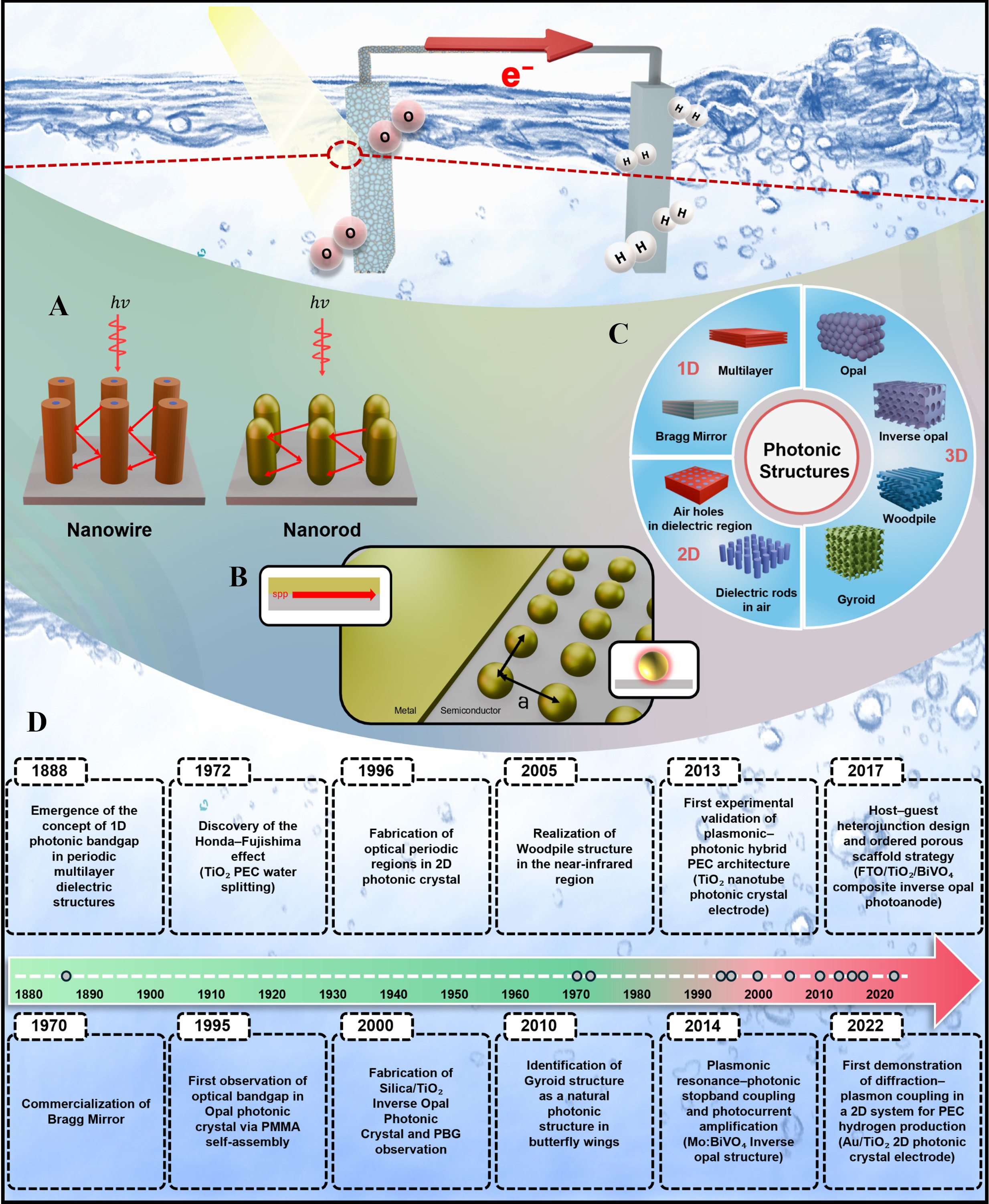
Figure 10. Mechanisms of SPP and LPR-based catalysis. (A) Light trapping in nanorod and nanowire; (B) SPP and LPR; (C) 1D ~ 3D Photonic structures; (D) Brief history of plasmonic-photonic hybrid structures. The emergence of the photonic bandgap concept[172], widespread adoption of Bragg Mirror[173], discovery of the Honda-Fujishima effect[174], experimental realization of 2D photonic crystals[175], development of opal and inverse opal photonic crystals[176], establishment of woodpile and gyroid architectures[177,178], and recent advances in plasmonic-photonic hybrid PEC photoelectrodes enabling enhanced light harvesting and hydrogen production[164,179-182]. hν: Energy of photon; 1D: one-dimensional; 2D: two-dimensional; PEC: photoelectrochemical; PMMA: poly(methyl methacrylate); PBG: photonic bandgap; SPP: surface plasmon polariton; LPR: lattice plasmon resonance.
Hybrid architectures combining nanoparticles with nanostructures enable simultaneous optimization of absorption and scattering. For example, Au nanoparticles-decorated BiVO4 inverse opal electrodes exhibited enhanced PEC activity through the synergistic broadband nanoparticle scattering and slow-photon effects from the inverse opal geometry[150].
Scattering enhancement can be optimized by controlling particle size, morphology, and spatial arrangement[151-154]. However, the PEC performance strongly depends on the balance between (σabs) and (σsca). In Au nanoparticle-modified BiVO4 photoanodes, particles with a diameter of 30nm achieve nearly a twofold enhancement in photocurrent, whereas larger particles (60 ~ 80 nm) result in reduced performance[155]. Overall, scattering enhancement is a design-governed mechanism in PEC systems, where optimal performance requires balanced control of absorption and scattering through particle size, morphology, and structural arrangement.
Effect of periodicity
In plasmonic nanostructures, periodicity determines the coupling efficiency between neighboring dipoles and the coupling conditions of diffraction modes[156]. Well-designed periodicity satisfies the phase-matching condition, thereby strengthening dipole-dipole coupling, reducing attenuation losses, and narrowing the resonance linewidth, leading to the formation of a high Q-factor and enhanced electromagnetic field localization[157]. As schematically illustrated in Figure 10B, propagating SPP modes and LPRs arise from collective coupling in periodic plasmonic arrays.
Periodic arrays promote the hybridization of SPPs and LSPRs, thereby enhancing light absorption and hot-carrier injection efficiency[158]. Moreover, periodic arrays enable precise and tunable control of plasmonic responses, allowing optimized periodicity to match the semiconductor bandgap with the resonance peak and thus maximize light-harvesting efficiency[159,160]. The resulting strong electromagnetic fields induce spatial separation of photogenerated electron-hole pairs[161].
However, excessively large periods may weaken field focusing or induce non-resonant modes, necessitating balanced designs and motivating a focus on multiscale and three-dimensional periodic plasmonic architectures that optimize light scattering, mode hybridization, and charge dynamics for PEC water splitting[162-164]. In addition, the integration of refractory and complementary metal-oxide-semiconductor (CMOS)-compatible plasmonic materials (e.g., TiN, HfN) with periodic arrays would represent a meaningful direction for further advancement[165].
Contribution of LPR in water splitting
As discussed above, conventional semiconductor photocatalysts are constrained by the SQ limit, narrow absorption range, and low quantum efficiency; however, LPR has recently emerged as a promising strategy to overcome these limitations[166]. LPR is a collective resonance phenomenon that occurs in periodic arrays of metal nanoparticles that form a much narrower and stronger resonance than individual particles, providing a high Q-factor and strong electromagnetic field amplification[167]. The unique properties of LPRs can significantly improve the photocatalytic performance of water-splitting reactions in many ways.
First, LPRs extend the light absorption into the visible and NIR, enabling more efficient utilization of photons beyond the intrinsic bandgap absorption limit of semiconductors. Deng et al. demonstrated that Cu-Pt nanoparticle lattices supporting SLRs exhibited up to 60% enhancement in hydrogen evolution reaction activity under white-light illumination compared to conventional LSPR-based catalysts[168]. Second, the ultraviolet absorption efficiency of wide-bandgap semiconductors can be further enhanced. Recently, TiN nanodisk arrays have been reported to support SLRs with narrower linewidths and more than an order of magnitude higher Q-factors than conventional LSPRs, which can facilitate efficient charge generation and separation in the UV and visible regions[54]. Third, the collective resonant coupling inherent in LPRs induces a strong electromagnetic field confinement, thereby markedly enhancing charge separation efficiency and suppressing carrier recombination. Li et al. reported a tenfold increase in photocurrent and up to an 18-fold enhancement in IPCE for a hematite nanorod array integrated with an Au nanohole lattice[68].
LPR-based photoelectrodes hold strong potential for achieving commercially viable, high-efficiency hydrogen production through high-Q resonance control, heterojunction design with diverse semiconductors, and the use of low-cost metals and composite materials[169], while future research is expected to further expand their commercial feasibility through materials innovation and scalable fabrication strategies.
Plasmonic-photonic hybrid structures
Conventional PEC photoelectrodes are fundamentally constrained by their narrow spectral absorption and inefficient charge separation[94]. To overcome these intrinsic limitations, the integration of photonic structures with plasmonic nanostructures has emerged as a promising next-generation strategy[123]. Figure 10C illustrates various plasmonic-photonic hybrid structures. Photonic architectures enhance light harvesting, charge transport, and catalytic activity by modulating light propagation while plasmonic-photonic hybrid designs further exploit the slow photon effect, internal multiple reflections, and efficient light trapping[170,171].
The historical development of photonic structures provides an essential framework for PEC applications [Figure 10D]. Specifically, this timeline highlights major breakthroughs: The emergence of the photonic bandgap concept[172], widespread adoption of Bragg Mirror[173], discovery of the Honda-Fujishima effect[174], experimental realization of two-dimensional photonic crystals[175], development of opal and inverse opal photonic crystals[176], establishment of woodpile and gyroid architectures[177,178], and recent advances in plasmonic-photonic hybrid PEC photoelectrodes[164,179-182].
To elaborate on these key developments, the concept of photonic structures originates from the theoretical work of Rayleigh in 1887, who described the formation of reflection bands in periodic multilayer dielectric media[172]. This concept was later formalized as the photonic bandgap by Yablonovitch and Jon in 1987[183]. Subsequently, one-dimensional (1D) multilayer Bragg reflectors became widely adopted in optical and laser devices from the 1970s onward as practical implementations of 1D photonic structures[173]. In 1996, two-dimensional (2D) photonic crystals based on air-hole silicon slabs were experimentally realized at near-infrared wavelengths[175]. Since the late 1990s, three-dimensional photonic crystals fabricated via colloidal self-assembly, including opal and inverse opal architectures, have been developed[176] and were later extended to woodpile and gyroid structures. Woodpile structures enable precise bandgap control, whereas gyroid structures provide isotropic band gaps and enhanced light-matter coupling[177,178].
The integration of photonic structures into PEC water splitting systems is a relatively recent development. Following the discovery of the Honda-Fujishima effect in 1972[174], systematic incorporation of photonic architectures into PEC electrodes only began in the 2010s. Early demonstrations included Au-integrated TiO2 nanotube photonic crystal photoelectrodes in 2013[182] and Au-decorated Mo-doped BiVO4 inverse opals in 2014, where strong coupling between plasmonic resonance and the photonic Bragg stopband significantly enhanced photocurrents[181]. In 2017, three-dimensional FTO/TiO2/BiVO4 composite inverse opal photoanodes were developed, simultaneously enhancing charge transport, charge separation, and light harvesting[180]. While more recently, in 2022, Au/TiO2 2D photonic crystal electrodes were reported, experimentally realizing diffractive-plasmon coupling for PEC hydrogen production[179].
Future research is expected to focus on narrowband spectral matching between SPR and PBG, polarization control, precise structural alignment, and integration of optical absorption with catalytic functionality to maximize solar to hydrogen efficiency. Such plasmonic-photonic hybrid systems offer a promising design pathway for scalable and highly efficient PEC water splitting[184].
DESIGN STRATEGY OF PLASMONIC PHOTOELECTRODES
Contact geometry
Direct contact
Physical vapor deposition-based techniques rely on evaporating or ejecting metal atoms under vacuum conditions for direct deposition onto semiconductor substrates, thereby providing high-purity interfaces and uniform coverage. Thermal evaporation has been employed to deposit Ag nanoparticles onto ZnO@CuO core-shell nanowires, resulting in homogeneous metal decoration and enhanced charge separation and light absorption [Figure 11A][185]. Sputtering has been applied to ZnO nanorod electrodes, where Au nanoparticle decoration led to more than a 50-fold enhancement in PEC photocurrent compared with bare ZnO [Figure 11B][186]. Moreover, electron-beam evaporation has been used to fabricate Ag nanorod arrays on ZnO thin films [Figure 11C][187]. Particularly, template-assisted assembly can be considered an extension of PVD, in which external templates (e.g., AAO pores, polystyrene bead arrays) are employed to form ordered and periodic nanoparticle arrays [Figure 11D]. Unlike simple deposition, this strategy allows excitation of SLR modes and plasmon-photonic coupling, thereby markedly improving wavelength selectivity and charge separation efficiency in PEC electrodes[188].
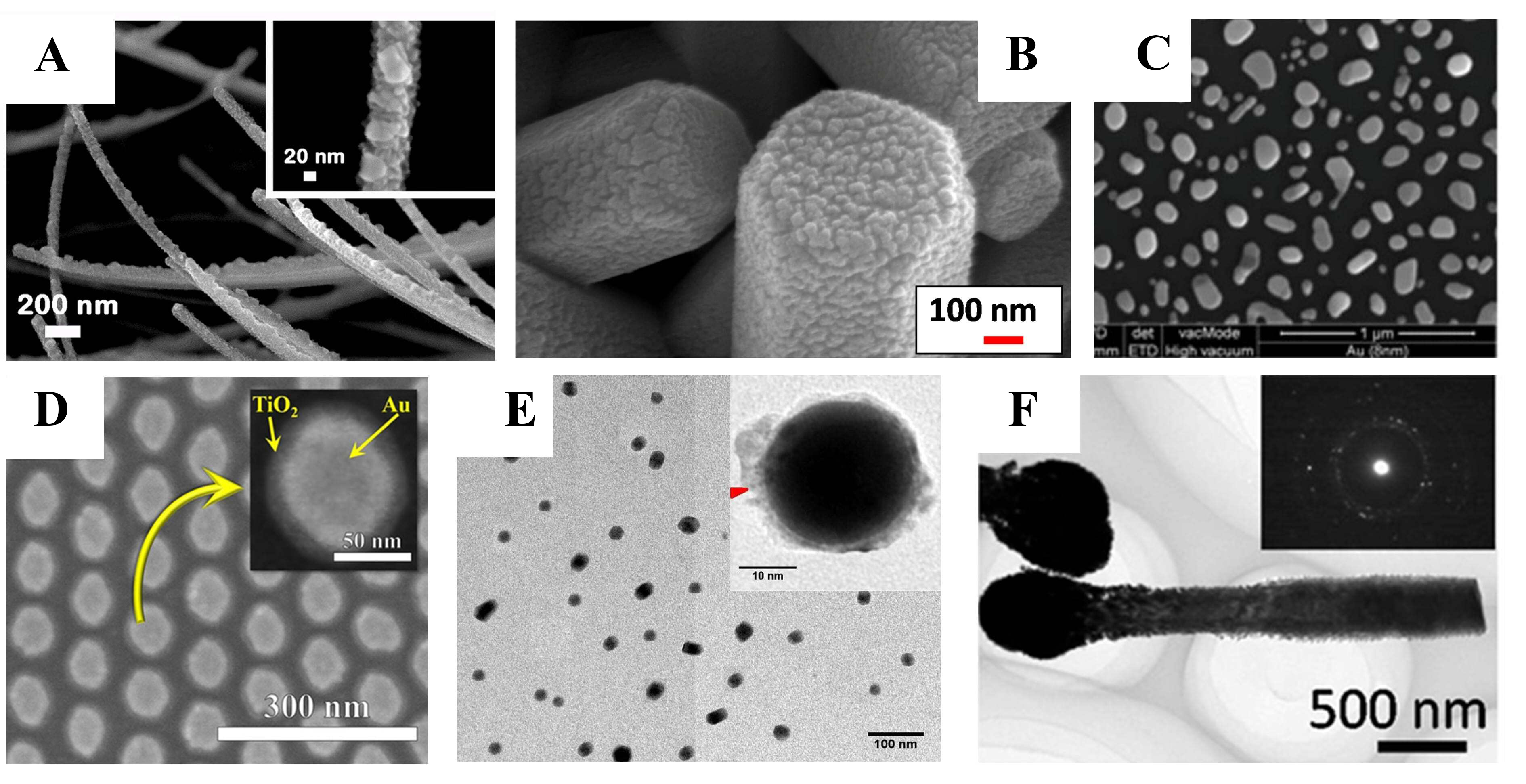
Figure 11. Direct contact formation strategies. (A) Thermal evaporation of Ag nanoparticles decorated ZnO@CuO core-shell nanowires[185]. Copyright 2023, published by Springer Nature; (B) Sputtering deposition of Au nanoparticles on ZnO nanostructured films[186]. Copyright 2021, published by Multidisciplinary Digital Publishing Institute (C) Formation of Au nanoparticles via E-beam evaporation followed by thermal dewetting[187]. Copyright 2022, published by Springer Science and Business Media LLC; (D) SEM image of Au nanodisc arrays fabricated by template-assisted assembly using an anodized aluminum oxide (AAO) ultrathin membrane mask[188]. Copyright 2020, reproduced with permission. Published by Wiley-VCH; (E) Au@ZnO core-shell nanoparticles prepared via Pulsed Laser Ablation Technique in chloroauric acid solution[189]. Copyright 2022, reproduced with permission. Published by Elsevier; (F) ZnO/Au heterostructure via photoreduction[190]. Copyright 2014, published by the American Chemical Society. SEM: Scanning electron microscopy.
Solution-based methods are advantageous due to their reduced reliance on complex instrumentation and the absence of surfactants. Pulsed laser ablation in liquid (PLAL) enables the generation of metal nanoparticles directly in liquid media, forming stable Au@ZnO core-shell structures without capping agents and allowing direct adhesion to substrates without impeding interfacial charge transfer [Figure 11E][189]. Photoreduction is another widely studied solution-phase approach, in which photoexcited electrons reduce metal ions (e.g., Au3+) adsorbed on semiconductor surfaces such as ZnO or TiO2, as demonstrated by the in situ formation of Au nanoparticles on ZnO nanorods under illumination [Figure 11F][190]. Together, these approaches enhance interfacial charge transfer and catalytic efficiency in PEC water splitting.
Indirect contact
When photoelectrodes and nanoparticles carry opposite charges, Coulombic attraction naturally drives their adsorption, leading to interfacial stabilization via charge neutralization. For instance, Han et al. functionalized CdS nanowires with mercaptoacetic acid to introduce negative surface charges, which facilitated the electrostatic adsorption of positively charged cetyltrimethylammonium bromide (CTAB)-stabilized Au, Ag, and Pt nanoparticles, yielding uniformly decorated nanostructures with significantly enhanced PEC activity [Figure 12A][191]. Electron transport in colloidally synthesized Au nanoparticles is improved through ligand exchange. In a representative LBL-assembled Au-Pt system, ligand exchange enabled metallic-level conductivity and a low overpotential (~ 66 mV) even at a Pt loading of 0.73 wt.% [Figure 12B][192]. Molecular bridging using small organic linkers enhances interparticle electronic coupling and charge transport. In particular, dithiol linkers have been demonstrated as an effective means to facilitate electron transfer between plasmonic clusters [Figure 12C][193].
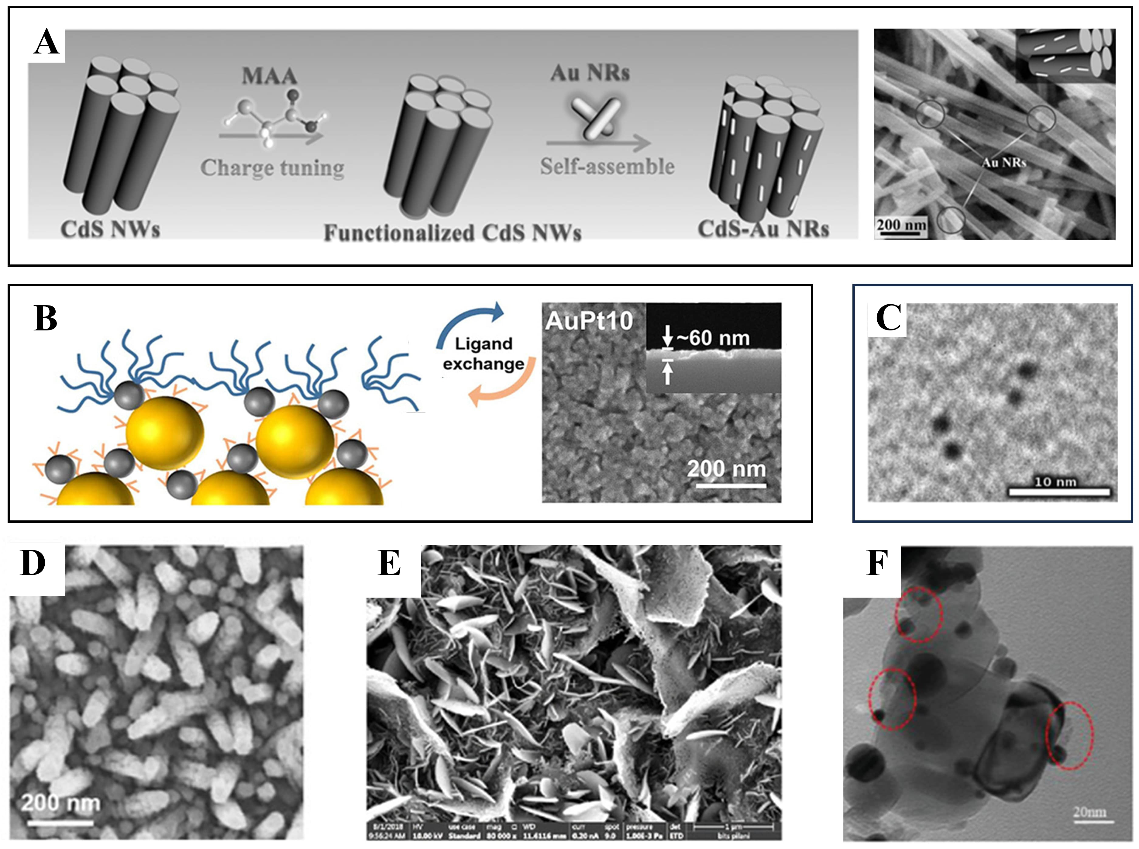
Figure 12. Indirect contact formation strategies. (A) Coulombic attraction-assisted assembly of Au NRs on CdS NWs[191]. Copyright 2017, published by Wiley-VCH; (B) Ligand-exchange-assisted LBL assembly of Au-Pt bimetallic films[192]. Copyright 2023, published by American Chemical Society; (C) Au nanocluster dimers linked via dithiol bridging[193]. Copyright 2018, published by American Chemical Society; (D) SEM image of InGaN nanorods surface-functionalized with Au nanoparticles[197]. Copyright 2020, published by Multidisciplinary Digital Publishing Institute; (E) FESEM image of α-Fe2O3 nanosheets prepared by the drop-casting method[198]. Copyright 2024, published by American Chemical Society. (F) TEM image of Au/Al2O3(NP)/TiO2 prepared by ALD[199]. Copyright 2020, published by Wiley-VCH GmbH. NW: Nanowire; NR: nano-rod; DETA: diethylenetriamine; NP: nano-particle; SEM: scanning electron microscopy; FESEM: field emission scanning electron microscopy; TEM: transmission electron microscopy; ALD: atomic layer deposition.
Surface functionalization represents another important method for stabilizing the metal-semiconductor interface. By introducing functional groups such as -COOH, -SO3-, or -NH2, or by applying polymeric coatings e.g., polystyrene sulfonate (PSS), polyethyleneimine (PEI)], the surface charge of nanoparticles can be tuned to enhance electrostatic adsorption onto semiconductors[194, 195]. However, excessive Au nanoparticle loading can suppress semiconductor light absorption due to shadowing effects[196]. Surface functionalized Au nanoparticle decoration represents an effective indirect contact strategy that simultaneously regulates interfacial stability and charge transfer efficiency, providing key design guidelines for PEC water [Figure 12D][197].
Physically, indirect contact can also be achieved via drop-casting, where nanoparticles form nanoparticle-on-mirror (NPoM) configurations that enable ligand-mediated hot-carrier generation and transfer [Figure 12E][198]. Alternatively, atomic layer deposition (ALD) enables the introduction of ultrathin dielectric spacers; in Au/TiO2 systems, an atomically controlled Al2O3 layer yields a well-defined Au/Al2O3/TiO2 architecture, illustrating a general strategy for tailoring plasmonic-semiconductor interfaces in PEC water-splitting [Figure 12F][199].
Nanostructured semiconductor effect
The integration of nanostructured semiconductors into plasmonic systems has emerged as a potent strategy to amplify light-matter interactions and optimize the performance of PEC and photocatalytic processes[200]. The unique size, shape, and surface-dependent properties exhibited by semiconductors at the nanoscale critically influence light absorption, charge carrier dynamics, and interfacial reactivity, thereby intensifying plasmon-induced phenomena[201]. Among the most significant benefits is the quantum confinement effect[202]. When the size of semiconductor particles approaches the exciton Bohr radius, discrete energy levels emerge, enabling tunable band gaps[203]. For instance, CdS@CdS core-shell quantum dots enable precise spectral alignment with plasmonic resonances through size and thickness control[204].
Moreover, nanostructures such as nanowires, nanorods, and mesoporous films induce light trapping via internal reflection and multiple scattering, which enhances photon absorption and increases optical cross-section[203,204]. Another notable advantage of nanostructured semiconductors is their high surface-to-volume ratio, which increases the density of surface reaction sites, promotes plasmon-induced surface reactions, and shortens the diffusion length of photogenerated charge carriers[205,206]. Furthermore, nanostructured semiconductors offer tunable defects and doping profiles[207]. Engineering surface defects or introducing selective dopants allows for mid-gap state formation, bandgap narrowing, or enhanced visible light absorption[208]. For example, Au-decorated BiVO4 photoanodes with oxygen vacancies establish strong metal-support interactions with Au nanoparticles, facilitate hot electron injection, and reinforce interfacial coupling[209]. Nanostructured semiconductors provide multifaceted advantages-enhanced light harvesting, improved charge separation, and reinforced interfacial reactivity-that collectively augment the performance of plasmonic architectures.
Representative LSPR-based nanostructures
Ordered and disordered LSPR-based nanostructures constitute two complementary plasmonic design strategies for PEC water splitting. Ordered LSPR-based nanostructures are defined as architectures in which metallic nanoparticles or nanoholes are periodically arranged to induce coupling between individual LSPR modes and diffractive orders[210]. Such periodicity gives rise to SLRs, with Q-factors on the order of several thousand, thereby enabling high-quality, wavelength-selective resonances. [Figure 13A][211]. In addition, ordered Au arrays fabricated on metal oxide photoelectrodes strongly amplify the near-field, suppressing electron-hole recombination and optimizing charge separation and injection pathways [Figure 13B][212]. These mechanisms manifested in practical PEC performance metrics, where ordered arrays exhibit several-fold enhancements in photocurrent density and IPCE over disordered counterparts, particularly at selected spectral regions [Figure 13C][200].
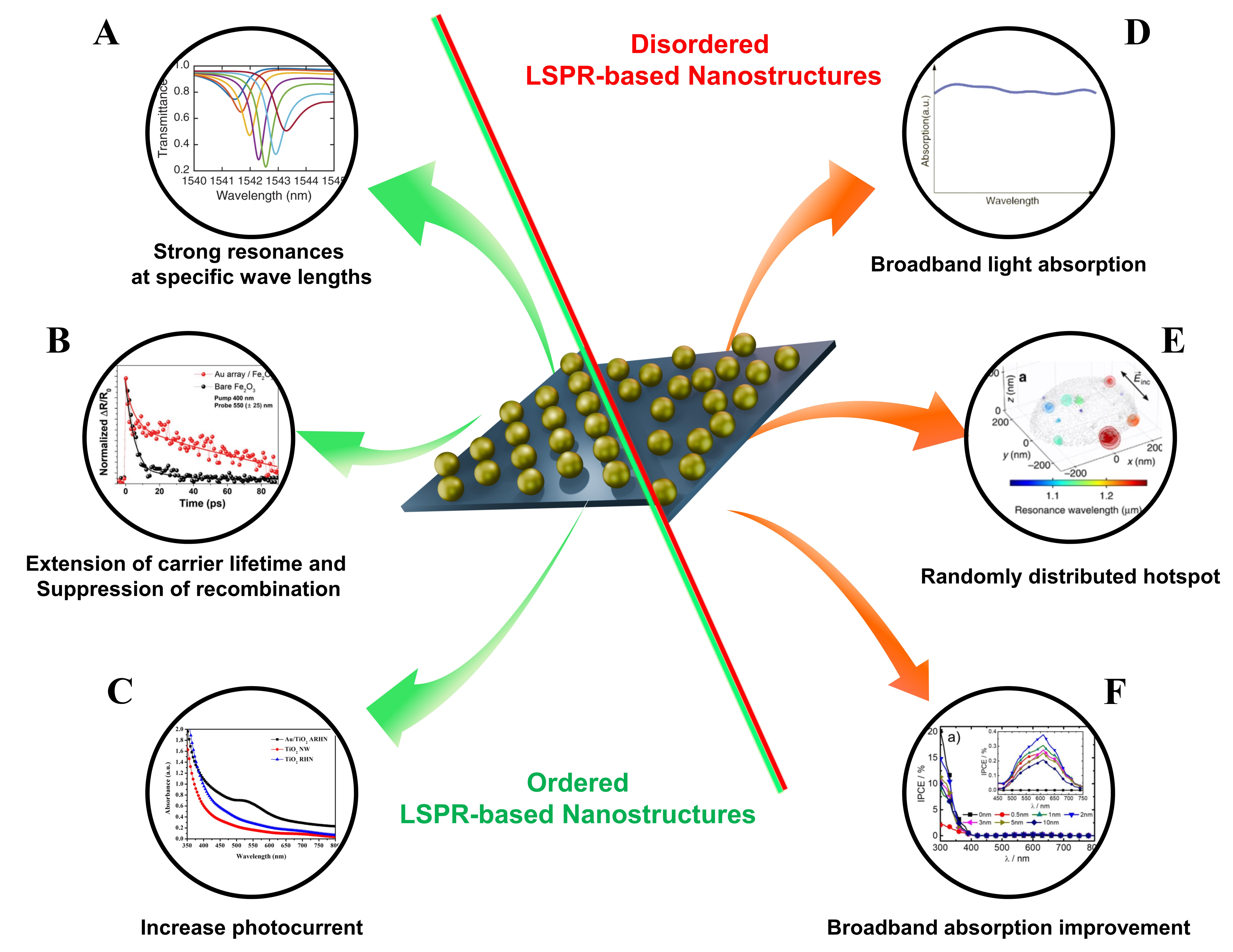
Figure 13. Comparison of ordered and disordered LSPR-based nanostructures. (A) Absorption of strong resonances at a specific wavelength[211]. Copyright 2021, published by Nature Publishing Group; (B) Transient absorption (TA) decay profiles at 550 nm for Au array/Fe2O3, showing suppressed short-time recombination and stabilized long-lived holes at the surface[212]. Copyright 2020, published by Wiley-VCH; (C) Absorption enhancement of TiO2 ARHN by scattering and visible-light absorption with photocurrent increase of Au/TiO2 ARHN by LSPR[200]. Copyright 2017, published by Springer Nature; (D) Broadband light absorption[217]. Copyright 2020, published by Springer Nature; (E) Randomly distributed plasmonic hotspots in a disordered gold nanosponge showing stochastic field localization across different resonance wavelengths[218]. Copyright 2018, published by Springer Nature; (F) IPCE spectra of Au NP-decorated TiO2 photoanodes formed by disordered LSPR nanostructures, showing broadband baseline enhancement across the visible range[219]. Copyright 2020, published by American Chemical Society. LSPR: Localized surface plasmon resonance; IPCE: incident photon-to-current efficiency; ARHN: hierarchical network deposited with Au nanoparticles; NP: nano-particle.
For instance, a system combining Au nanohole arrays with α-Fe2O3 nanorod electrodes exhibited IPCE enhancements of approximately 18-fold in the sub-bandgap region and 13-fold near 425 nm[212], while ordered Au metasurfaces demonstrated ultrahigh-quality resonances with Q ≈ 2340, which critically contributed to electromagnetic field enhancement and photocurrent amplification[211].
In contrast, disordered LSPR nanostructures refer to disordered metasurfaces in which particle size, shape, and spacing are non-uniform or randomly distributed[213]. In two-dimensional arrays, non-uniform distributions can be generated through self-assembly techniques such as random sequential adsorption (RSA), while correlated disorder designs enable the introduction of local irregularities while preserving the average interparticle spacing, allowing continuous tuning of scattering responses between periodicity and disorder[214-216]. The coexistence of variations in size, morphology, and spacing induces broadband plasmonic resonances, thereby enhancing absorption across the entire visible region (450-750 nm) [Figure 13D]. Au nanoparticles formed on TiO2 via thermal dewetting exhibited size-dependent SPR peaks; nevertheless, the PEC photocurrent consistently appeared near 600 nm, indicating a broadband response[217]. Moreover, random arrangements generate electromagnetic hotspots at unpredictable locations, as evidenced by long-lived localized plasmon modes confined within 10-20 nm pores of dealloyed Au-Ag nanosponges [Figure 13E][218]. Unlike ordered structures that provide sharp enhancements at specific wavelengths, disordered configurations contribute to a stable enhancement of the photocurrent baseline across the broadband region [Figure 13F][219].
In conclusion, ordered and disordered LSPR-based nanostructures provide complementary plasmonic enhancement strategies for PEC water splitting. Ordered architectures enable high Q-factors, wavelength-selective field enhancement, whereas disordered configurations offer broadband absorption and stable photocurrent amplification. Together, these design paradigms underscore the importance of tailoring plasmonic nanostructures for efficient solar-driven hydrogen production.
Representative SPP-based nanostructures
In PEC water-splitting, SPPs constitute a key concept underlying various nanostructures designed to maximize light absorption and charge transfer and can be broadly classified into ordered and disordered architectures that exhibit fundamentally different light-matter interaction regimes[43]. Ordered SPP nanostructures employ periodic metallic patterns to selectively excite propagating SPP modes, resulting in narrow resonance bandwidths, high Q-factors, and wavelength-selective, stable optical responses[149, 220]. In contrast, disordered SPP nanostructures, composed of non-periodically distributed metal nanoparticles or clusters, support broadband SPP-like modes with probabilistically distributed electromagnetic hotspots, enabling strong near-field localization over a wide spectral range[221-223].
These distinct interaction regimes translate directly into different PEC performance characteristics. Ordered architectures, exemplified by Au nanohole/hematite (α-Fe2O3) nanorod photoelectrodes, exhibited over an order-of-magnitude enhancement in photocurrent density and pronounced IPCE improvements at specific wavelengths due to SPP-induced waveguide modes[68]. Conversely, disordered Ag/TiO2 nanoplates and MgB2 nanosheet assemblies achieved broadband photocurrent enhancement, ~ 5% conversion efficiency, and stable hydrogen[224]. Rather than representing opposing strategies, periodicity and randomness should be regarded as complementary design parameters that can be selectively employed or combined depending on targeted PEC performance objectives.
Density functional theory analysis of surface reactions
Density functional theory (DFT) constitutes a pivotal tool in the study of plasmonic photoelectrodes, enabling atomic-scale elucidation and quantitative interpretation of electronic structures, interfacial charge transfer, electron density distributions at active sites, adsorption energies, and reaction pathways[225]. In particular, by providing insights into hot electron injection, band alignment modulation, and the stability of surface intermediates at plasmonic metal-semiconductor interfaces, DFT establishes the fundamental basis for enhancing PEC efficiency[226]. These insights are typically obtained through analyses of representative reactive units within PEC electrodes, including metal-semiconductor nano-heterojunctions[226,227], alloy-based nanoparticles[228], and nanocluster-molecule interfaces[229].
In the Au/Fe2O3 interface, DFT calculations revealed that Au clusters bound to the Fe2O3 (001) surface generate new electronic states near the conduction band minimum (CBM), facilitating the migration of photoexcited electrons into the Fe2O3 conduction band[226]. Moreover, for Au nanocluster-H2O gap structures, linear-response time-dependent DFT (LR-TDDFT) calculations demonstrated that dual-cluster gaps induce stronger electromagnetic field enhancement and direct charge transfer[230]. In Ag-Au alloy/TiO2 electrodes, DFT identified (Ag0.6Au0.4) as the optimal composition for maximizing electron injection and OER activity[231]. Thus, DFT functions as a central pillar in the next-generation design of plasmonic nanostructure-based PEC hydrogen production systems, delivering its greatest impact when employed synergistically with experimental validation[232].
AI-assisted designs
Artificial intelligence (AI) has become a powerful tool for the design and optimization of plasmonic nanostructures in PEC water splitting, addressing the complexity of light absorption, charge recombination, interfacial defects, and nonlinear structure-performance relationships that limit traditional synthesis and physics-based simulations[233-237]. AI-driven methodologies, particularly machine learning (ML) and deep learning (DL), overcome these limitations by providing rapid predictive capabilities[238,239].
Deep neural networks (DNNs), trained on large simulation datasets, have learned the intricate correlations between structural parameters and optical responses, predicting near-field electric distributions and far-field scattering spectra with 3-5 orders of magnitude faster computation (103 ~ 105 times) compared to conventional FDTD or FEM simulations[240]. Reinforcement learning (RL) and data-efficient strategies such as semi-supervised learning (SSL) further enhance structural optimization in limited-data regimes, balancing performance objectives with experimental or computational costs[241,242].
Beyond data-driven models, physics-aware frameworks that integrate DFT and ab-initio molecular dynamics (AIMD) with ML offer accurate predictions of hot-electron generation, band alignment, and interfacial charge-transfer dynamics at plasmonic-semiconductor junctions[243-245]. Representative demonstrations include ML-based prediction of plasmonic coupling from optical color[246], AI-assisted atomic-level cluster growth control[247], and inverse design of broadband metamaterials[248]. Overall, AI-assisted design frameworks overcome the computational limits of conventional simulations by integrating physics-based insights with data, enabling optimal plasmonic nanostructure design for high-performance PEC water splitting.
KEY BREAKTHROUGHS IN PLASMONIC SOLAR WATER SPLITTING
Spatially coupled plasmonic nanoparticles
In Figure 14A, kelvin probe force microscopy (KPFM) mapping directly visualizes a pronounced surface photovoltage (SPV) at a dimeric Au-TiO2 junction under illumination, which originates from LSPR-induced hot electron injection from Au into TiO2 across the Au-TiO2 Schottky interface. In contrast, the complementary hot holes remain confined within the Au nanoparticle[249,250]. This SPV response is particularly enhanced in closely spaced Au-TiO2 dimers, where strong plasmonic near-field coupling within the nanogap generates intense local electromagnetic fields, leading to increased hot-carrier generation and more efficient interfacial charge separation compared to isolated nanoparticles[251,252].
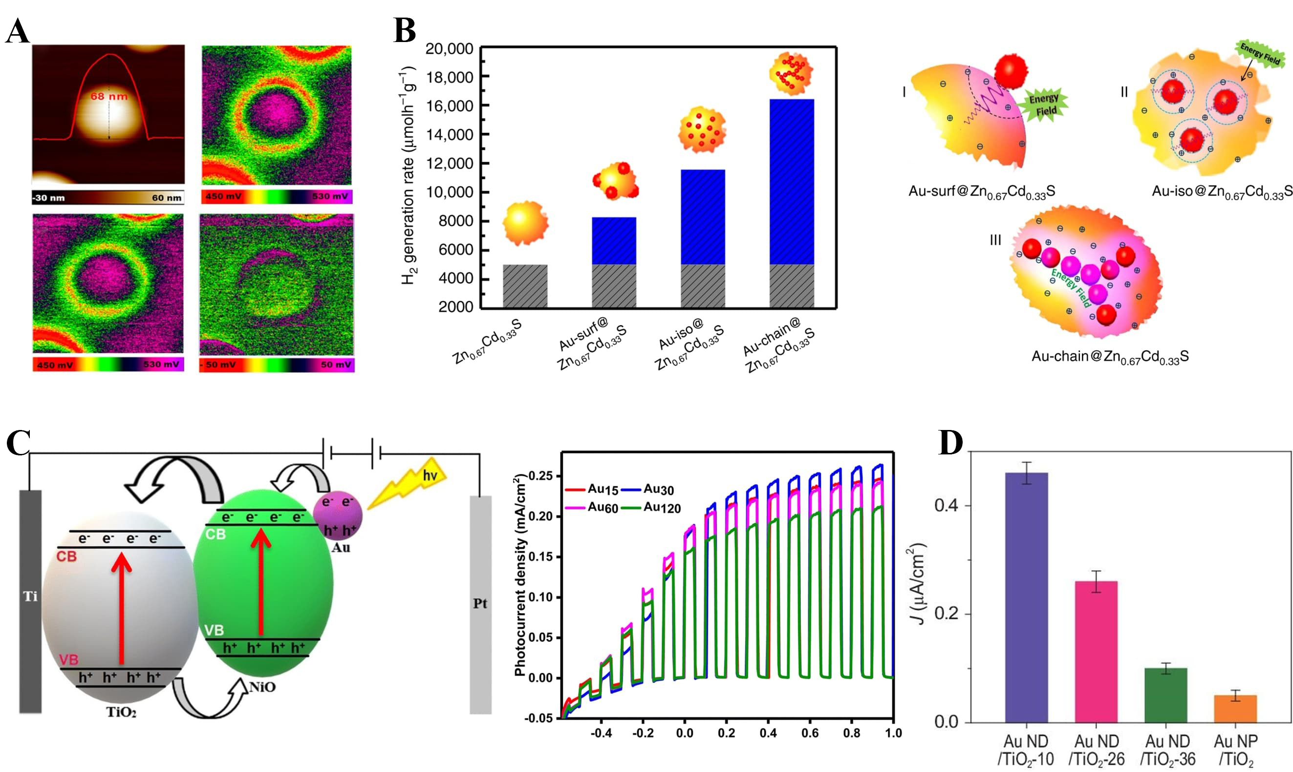
Figure 14. Spatial coupling of plasmonic Au nanoparticles on enhanced charge separation (A) Spatially resolved potential mapping of a single Au nanoparticle on a TiO2 surface[250]. Copyright 2017, published by the American Chemical Society. (B) H2 evolution rates of Zn0.4Cd0.6S with different Au configurations and corresponding schematics of surface-decorated, isolated, and chain-like Au assemblies[114]. Copyright 2019, published by Nature; (C) Energy-band diagram and photocurrent responses of Au-sensitized NiO/TiO2 heterojunction photoelectrodes with varying Au loadings[257]. Copyright 2023, published by the Royal Society of Chemistry; (D) Bar graph of steady-state photocurrent density (J) for various Au/TiO2 photoanode configurations[258]. Copyright 2020, published by Oxford Academic. CB: Conduction band; VB: valance band; hν: energy of photon; ND: nanorod; NP: nano-particle.
Figure 14B extends this principle to catalyst ensembles, showing that spatially coupled Au assemblies such as linear nanochains generate stronger near-field enhancement and more efficient hot-electron transfer than isolated nanoparticles, yielding nearly 3.5-fold higher visible-light-driven H2 evolution on Zn0.67Cd0.33S[114,252]. This spatial-design principle is general, as Au-decorated TiO2 photoelectrodes also exhibit enhanced oxygen evolution under visible illumination, particularly when combined with a p-type NiO layer that facilitates hole extraction and suppresses recombination[253-255].
Figure 14C illustrates device-level engineering in Au/NiO/TiO2-based photoanodes, where the photocurrent increases with Au loading and reaches a maximum at an optimal coverage (Au30/NiO/TiO2)[255]. In this tri-layer architecture, Au nanoparticles enhance visible-light absorption via LSPR and inject plasmonically generated hot electrons into TiO2, while NiO (or NiOx) facilitates hole extraction and suppresses charge recombination, collectively leading to enhanced photocurrent generation[256]. Similar synergistic effects are observed in bimetallic Au-Ni cocatalyst systems integrated with TiO2 nanotube photoanodes, where intimate Au-Ni-TiO2 interfacial contact enables directional charge separation and yields significantly improved photocurrent density and stability compared with single-metal photoanodes[257].
Figure 14D emphasizes the importance of nanoscale spatial engineering in plasmon-enhanced photoelectrochemical systems. Periodic Au nanodot arrays with ~ 10 nm interdot spacing form strongly coupled plasmonic hotspots at the Au-TiO2 interface, generating concentrated electromagnetic fields that enhance local carrier generation via near-field coupling[114,256]. Consequently, TiO2 electrodes patterned with dense, ordered Au nanodot arrays exhibit an order-of-magnitude higher photocurrent than those with randomly dispersed Au nanoparticles[114,258]. In contrast, increased interdot spacing or random nanoparticle distributions weaken near-field coupling and diminish this enhancement, underscoring that precise spatial arrangement-beyond simple loading-is critical for maximizing plasmon-induced charge separation and photoelectrochemical efficiency[114,259]. In addition to structural engineering, heteroatom doping and oxygen vacancy creation in TiO2 have also been explored to induce LSPR-like behavior. These strategies introduce free charge carriers or mid-gap states, facilitating visible-light absorption and plasmonic charge dynamics. Notably, such effects have been demonstrated even in traditionally non-plasmonic semiconductors such as TiO2. These material-level strategies align with recent efforts focusing on plasmonic field engineering and spatial coupling to maximize hot-electron utilization in PEC water splitting[260,261].
Plasmonic heterostructures
Figure 15A illustrates plasmon-driven charge transfer in an Au-g-C3N4 system suspended in triethanolamine (TEOA), where LSPR excitation in Au nanoparticles generates hot electrons injected into the g-C3N4 conduction band, while hot holes are scavenged by TEOA, enabling Au to act as both an optical antenna and an electron shuttle for H2 evolution. Under visible-light illumination (> 420 nm), the Au-g- C3N4 composite exhibits nearly an order-of-magnitude higher hydrogen evolution than bare g- C3N4, and this activity is retained within a narrowed excitation window of 420 ~ 465 nm, extending into the red-edge region (450 ~ 600 nm) where pristine g-C3N4 is inactive, thereby confirming a plasmon-driven rather than band-gap-driven mechanism[95,262].
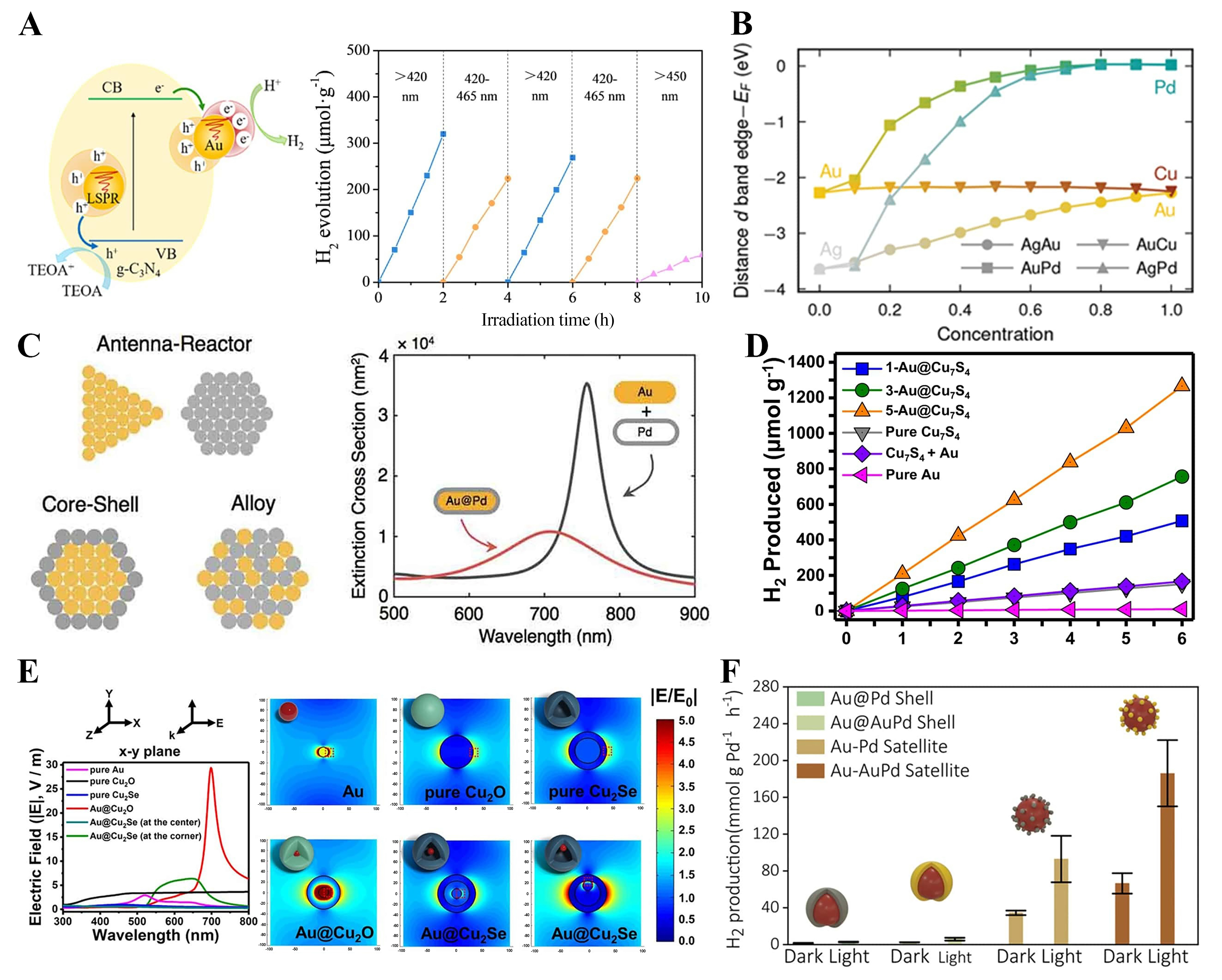
Figure 15. Au-Based Plasmonic Heteronanostructures for Water Splitting (A) Plasmon-induced charge separation mechanism in Au-decorated g-C3N4 under visible-light irradiation[95]. Copyright 2022, published by the Elsevier; (B) the distance between the band edge and the Fermi level[264]. Copyright 2020, published by the Wiley; (C) Plasmonic nanoarchitectures-antenna-reactor, core-shell, and alloy-depicted alongside extinction spectra of Au and Au@Pd nanostructures[265]. Copyright 2019, published by the Taylor & Francis; (D) Experimental H2 production rates of Au-decorated CuxS4 nanostructures, showing compositional and LSPR[267]. Copyright 2024, published by the Springer Nature; (E) FDTD-simulated near-field enhancement spectra and spatial electric-field distributions of Au-based core-shell heterostructures[268]. Copyright 2022, published by the American Chemical Society; (F) Comparison of light- and dark-driven H2 evolution for Au@Pd core-shell and core-satellite photocatalysts[263]. Copyright 2022, published by the Wiley. TEOA: Triethanolamine; EF: Fermi Leve; LSPR: localized surface plasmon resonance; FDTD: finite-difference time-domain.
Figure 15B demonstrates that alloying Au with Pd, Cu, or Ag systematically tunes plasmonic charge-transfer energetics through changes in the ECB ~ EF offset and intrinsic optical constants, highlighting alloy composition as a critical design parameter. Increasing Pd content enlarges the ECB ~ EF offset to ~ 1 eV, favoring efficient hot-electron injection, whereas Au-Cu alloys exhibit a plateaued offset and Ag-rich alloys collapse the driving force, thereby quenching plasmon-assisted charge extraction[263]. These trends originate from alloy-induced modifications in the real and imaginary permittivity, which shift interband transition thresholds and broaden plasmon resonance linewidths, demonstrating that intrinsic optical properties-beyond nanostructure geometry-critically govern plasmonic charge-transfer energetics and must be explicitly considered in plasmonic catalyst design[264].
Figure 15C compares the extinction behavior and plasmonic functionality of three Au-Pd architectures-antenna-reactor dimers, core-shell particles, and atomically mixed alloys-showing that nanoscale architecture critically governs near-field localization, hot-carrier generation, and photocatalytic performance. Antenna-reactor dimers exhibit a sharp, red-shifted LSPR (~ 780 nm) due to strong dipolar coupling at the Au-Pd junction, generating intense localized near-fields on Pd sites and yielding the highest H2 evolution activity[265,266]. In contrast, core-shell structures suffer plasmon damping from Pd shells, while fully alloyed Au-Pd nanoparticles experience stronger nonradiative losses that suppress near-field enhancement, resulting in lower activity[263,266]. Accordingly, photocatalytic performance follows the hierarchy antenna-reactor > core-shell > alloy, highlighting the importance of rational plasmonic-catalytic junction design for efficient hot-carrier utilization.
Figure 15D shows that increasing the number of embedded Au cores in Au@Cu1.9S photocatalysts markedly enhances plasmon-driven H2 evolution, with a five-core yolk-shell structure reaching ~ 115 μmol g-1 h-1 after 6 h, while single-core, Au-free, or physically mixed Au-Cu1.9S systems remain far less active[267]. This enhancement stems from the increased density of plasmonic excitation centers and expanded metal-semiconductor interfacial area, enabling cumulative hot-electron injection and strong interfacial field localization dictated by the core-shell geometry, thereby demonstrating that intimate nano-heterojunction embedding is essential for efficient plasmon-driven catalysis[267].
Figure 15E illustrates Simulated near-field enhancement (|E/E0|) shows that interfacial architecture governs plasmonic energy localization, with Au@Cu2Se exhibiting a > 5-fold field enhancement at ~ 700 nm (LSPR), whereas Au@Cu2O displays only a modest response near 550 nm[268]. Spatial field maps reveal that Au@Cu2Se yolk-shell nanoparticles form an intense ring-shaped hotspot at the Au-Cu2Se interface, in contrast to delocalized fields in Cu2Se and metal-confined hotspots in Au, thereby enabling efficient hot-electron transfer into the Cu2Se shell and accounting for the superior charge utilization and highest H2 quantum efficiency[267,268].
Figure 15F shows that plasmon-driven H2 evolution is negligible in the dark but strongly enhanced under illumination in Au-Pd satellite assemblies, which produce ≈ 8 nmol g-1 Pt h-1 about four times higher than Au@Pd core-shell catalysts[269]. This enhancement arises from intense plasmonic hotspots in Au-Pd nanogaps and discretely partitioned Pd islands that provide accessible H-adsorption sites while avoiding plasmon damping, enabling efficient hot-carrier transfer from Au to Pd[263, 269]. In contrast, continuous Pd shells damp the Au LSPR and suppress field localization, underscoring cocatalyst partitioning as a key structural parameter for efficient plasmon-driven hydrogen evolution[270]. These findings are in line with recent comprehensive reviews on single-atom plasmonic hybrids and multichannel charge transfer schemes for bond activation[271, 272].
Realization of interfacial phenomena in plasmon-enhanced photocatalysis
Figure 16A shows that loading plasmonic or transition-metal cocatalysts enables wide-bandgap TiO2 to operate under visible light, where bare TiO2 is inactive. Among various metals, Cu/TiO2 exhibits the highest H2 evolution via efficient hot-electron injection and suppressed recombination, as small Cu0/Cu+ clusters act as electron sinks and hole scavengers while extending visible absorption through interfacial charge-transfer states. Consequently, Cu/TiO2 achieves H2 evolution rates ~ 16× higher under UV and ~ 3× higher under visible light than pristine TiO2, whereas Fe-, Zn-, and Ce-modified TiO2 show negligible enhancement[273].
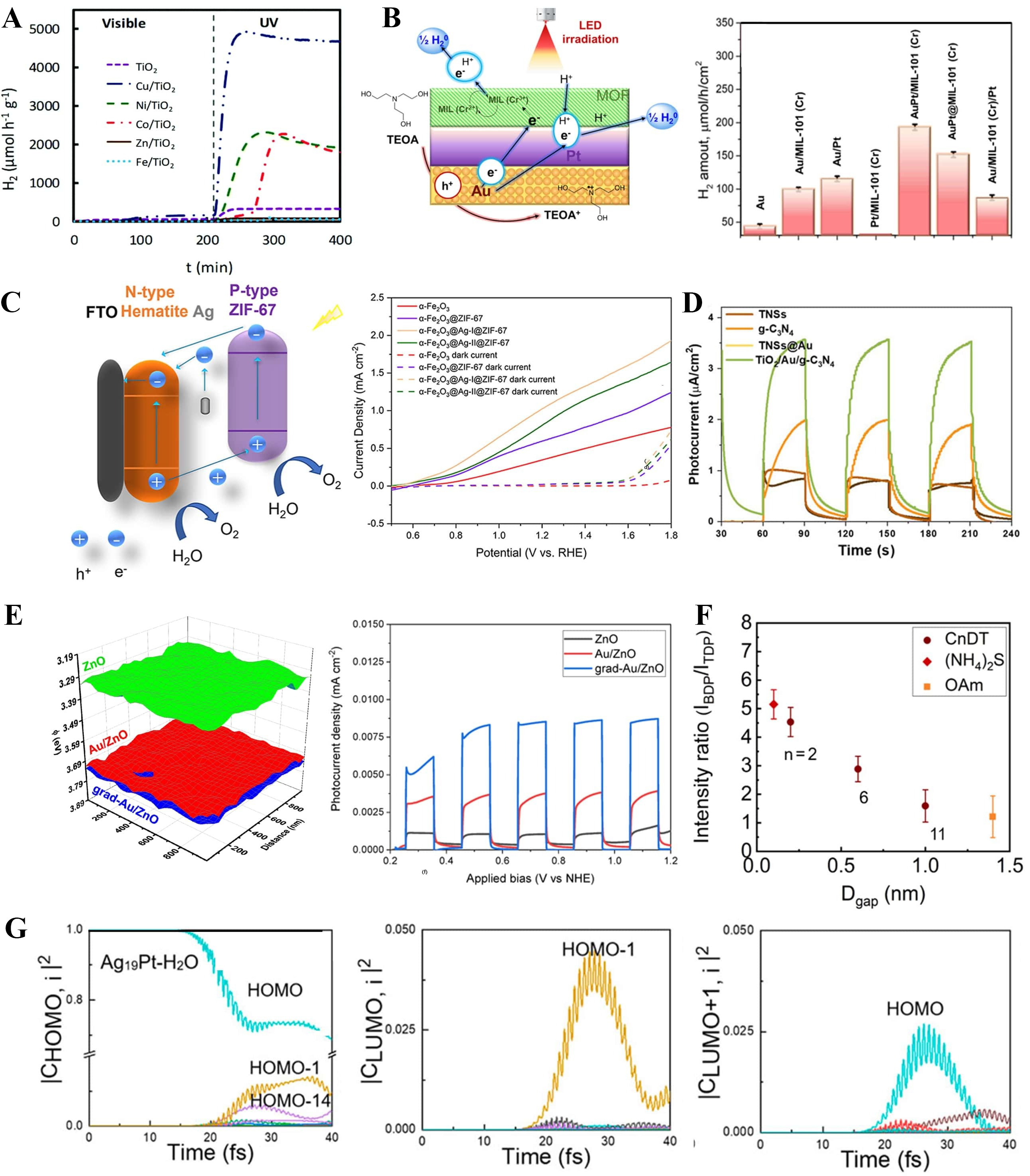
Figure 16. Plasmon-induced interfacial phenomena realizations (A) Hydrogen evolution profiles under visible and UV illumination using various metal-semiconductor systems[273]. Copyright 2021, published by the Royal Society of Chemistry; (B) Schematic of a MOF-supported Au-based plasmonic system and corresponding H2 generation performance[274]. Copyright 2020, published by the American Chemical Society; (C) Photoelectrochemical cell based on p-n junction and corresponding J-V curves under simulated solar illumination[276]. Copyright 2023, published by the Elsevier; (D) Chopped-light transient photocurrent responses of plasmonic-semiconductor composites[275]. Copyright 2022, published by the Frontiers; (E) Structural modulation of ZnO-based photoelectrodes and their photocurrent responses[277]. Copyright 2023, published by the Multidisciplinary Digital Publishing Institute; (F) Intensity ratio of bonding (top) vs. antibonding (gap) modes in plasmonic dimers as a function of interparticle gap size and linker molecules[279]. Copyright 2024, published by the American Chemical Society; (G) Time-resolved charge density dynamics of HOMO and LUMO states under hot electron excitation in an Ag19Pt-H2O cluster[280]. Copyright 2022, published by the Frontiers. UV: Ultraviolet; LED: light-emitting diode; TEOA: triethanolamine; MOF: metal organic framework; FTO:RHE: ZIF: zeolitic imidazolate framework; TNS: titanate nanosheet; NHE: normal hydrogen electrode; HOMO: highest occupied molecular orbital; LUMO: lowest unoccupied molecular orbital; MIL: Materials of Institute Lavoisier; J-V: current density-potential; BDP: bonding dipolar plasmon; TDP: transverse dipolar plasmon.
Figure 16B demonstrates a hierarchical plasmonic-MOF (metal organic framework) composite strategy in which a plasmonic Au core embedded in a porous MOF scaffold [e.g., Materials of Institute Lavoisier (MIL)-101(Cr)] enables efficient light harvesting and charge management. Under visible-NIR illumination, LSPR excitation in Au generates hot electrons that are injected into the MOF framework or Pt cocatalyst sites, leading to markedly enhanced H2 evolution compared with bare Au, with further improvement upon incorporation of a second metal (Ag or Pt)[274]. In particular, Au/Pt-MOF architectures sustain strong plasmon-polariton modes and stabilized interfaces that facilitate hot-electron transfer, broaden solar utilization into the NIR region, and deliver superior activity and durability relative to Au- or Pt-only systems[274,275].
Figure 16C demonstrates the extension of plasmonic design to integrated photoelectrodes using a ternary heterojunction photoanode comprising n-type α-Fe2O3, a p-type Co-based MOF overlayer [zeolitic imidazolate framework (ZIF)-67], and interfacial plasmonic Ag nanoparticles. Ag LSPR enhances visible-light absorption, while the Fe2O3/ZIF-67 p-n junction drives directional charge separation and suppresses recombination, resulting in the highest photocurrent and improved stability in current density-potential (J-V and chopped-light measurements. These results highlight that plasmonic heterojunction engineering effectively enhances charge separation and oxygen evolution in water-splitting photoelectrodes[276].
Figure 16D presents the dynamic on/off photoresponse of a plasmonic Z-scheme photocatalyst under chopped illumination, showing that the ternary titanate nanosheets (TNSs)-Au-g-C3N4 composite delivers the highest and most stable photocurrent among all configurations[275]. This enhancement arises from Au-mediated Z-scheme charge transfer, which directs electrons to the reduction side for H2 evolution while retaining holes on the oxidation side for O2 evolution, thereby confirming the effectiveness of interfacial plasmonic mediators in promoting both half-reactions[275].
Figure 16E compares ZnO nanorods with uniform and gradient Au doping, showing that spatially controlled dopant distributions critically influence plasmonic photoelectrode performance. In gradient Au-ZnO, surface-enriched Au maximizes near-field overlap with the photoactive region and strengthens the built-in electric field, yielding the highest photocurrent in J-V measurements by enhancing directional charge separation and suppressing recombination. These results demonstrate that dopant-gradient engineering effectively couples plasmonic field localization with internal electric-field control to improve solar-driven hydrogen and oxygen evolution[277]. Moreover, such strategies align with broader approaches used to induce plasmonic behavior in wide-bandgap metal oxides like TiO2 and ZnO, where heteroatom doping or the creation of oxygen vacancies introduces mid-gap states or localized free carriers. These modifications facilitate visible or near-infrared LSPR activation, thereby enhancing light absorption and hot-carrier generation even in originally non-plasmonic hosts.
Figure 16F links photoluminescence metrics and nanoscale coupling to plasmonic photocatalytic performance, showing that higher band-edge-to-trap-state photoluminescence (PL) spectroscopy intensity ratios-achieved via surface passivation-indicate reduced recombination, prolonged carrier lifetimes, and improved hydrogen and oxygen evolution[278]. In addition, shrinking metallic nanogaps induces hybridized bonding and antibonding plasmon modes whose intensity ratios track near-field coupling strength, as visualized in gold nanoparticle superlattices, where sub-nanometer gaps yield extreme field confinement and enhanced hot-carrier generation that promotes efficient interfacial electron injection[279].
Figure 16G illustrates plasmon-induced ultrafast charge-transfer dynamics in an Ag19Pt-H2O cluster, where a single Pt atom introduces multichannel electron-transfer pathways that rapidly populate the LUMO from multiple occupied orbitals upon photoexcitation. These parallel transfer routes drive O-H bond dissociation within ~ 40 fs, whereas the pure Ag20-H2O cluster lacks such dynamics and shows no ultrafast bond cleavage, highlighting the decisive catalytic role of Pt incorporation. Overall, plasmon excitation in Ag-Pt single-atom systems enables not only hot-electron injection but also multichannel charge-transfer processes that accelerate bond activation[280]. These findings resonate with emerging strategies utilizing single-atom sites to control multichannel electron transfer for plasmon-activated bond cleavage, as discussed in recent high-level reviews[271,272].
CHALLENGES AND OUTLOOKS
Challenges
Here, a summary of current challenges in plasmonic solar water splitting is given. First, there is no unified mechanism of plasmonic photocatalysis; therefore, theoretical ultimate limit is not clear yet. Therefore, in the development, there are ambiguities in the performance. Second, there is an uncertainty in the morphological optimization of plasmonic components as well as their arrangement. As overall plasmonic enhancement comes from the combination of the near-field, diffractive, far-field (Mie-like), and photonic hybridization effects, it is hard to achieve sufficient optimization. For development, it costs more time than other systems. Finally, as efficient interfacial charge-transfer and corresponding damping issues exist, the interfacial chemical structure is essential. However, in the plasmonic system, optimizations are not certain, which hinders the development of plasmonic-enhanced catalysis systems.
Outlooks
By achieving full optimization in the future, which leads to overcoming challenges, the following things are expected as benefits. The conventional band edge-limited absorption would be conquered. As a result, a broadband absorbable photoelectrode for covering AM 1.5G could be realized. This is consistent with the previously suggested theoretical expectations that bypass the SQ limit, which indicates an economically efficient water-splitting system. Partial realization in literature gives more potential to this argument. Moreover, the next-generation hydrogen society could get closer. Besides, the development of the plasmonic photoelectrode stimulates development in adjacent fields, such as solar-to-fuel conversions and sensing.
CONCLUSIONS
In this review, various plasmon-enhanced photocatalytic mechanisms are introduced, and methodological aspects are widely discussed. As water splitting through solar energy is promising for power-free operation, not only for the elimination of carbon-based waste burden, but also for the technological potential of overcoming current water-electrolysis technologies, improvement of performance is desired. As various forms of plasmon resonance, such as LSPR, SPP, and LPR, can be utilized, the mechanisms for their interaction with semiconductors have already been investigated, although optimization matters. As described in the manuscript, various attempts are also being made to optimize plasmon-induced interfacial phenomena in terms of compositional and morphological aspects. Recent approaches have also incorporated computational techniques like DFT and machine learning. These approaches provide results interpretation via a quantum perspective and the design strategies for photocatalytic materials. Based on the combination of computational and experimental techniques, a deeper understanding of the plasmon-enhanced catalysis is provided. Various aspects of current approaches ensure continued technological advancements in the plasmon-enhanced water splitting field. The content presented in this paper would work as a one-way finder for interested researchers in the field of plasmon-enhanced catalysis.
DECLARATIONS
Author’s contributions
Writing-original draft: Moon, C. W.
Writing-review & Editing & Collecting the literature: Kim, M.; Go, H. S.; Lee, J. Y.; Kim, Y. K.
Supervision & Conceptualization & Data Curation: Moon, C. W.
Availability of data and materials
Not applicable.
AI and AI-assisted tools statement
Not applicable.
Financial support and sponsorship
This research was supported by Korea Basic Science Institute (National Research Facilities and Equipment Center) grant funded by the Ministry of Science and ICT (No. RS-2024-00402822), the National Research Foundation of Korea (NRF) grant funded by the Korea government (MSIT) (RS-2025-00555609), and by Soonchunhyang University Research Fund.
Conflicts of interest
The authors declare that there are no conflicts of interest.
Ethical approval and consent to participate
Not applicable.
Consent for publication
Not applicable.
Copyright
© The Author(s) 2026.
REFERENCES
1. Møller, K. T.; Jensen, T. R.; Akiba, E.; Li, H. Hydrogen - a sustainable energy carrier. Prog. Nat. Sci.-Mater. 2017, 27, 34-40.
2. Budama, V. K.; Johnson, N. G.; Ermanoski, I.; Stechel, E. B. Techno-economic analysis of thermochemical water-splitting system for Co-production of hydrogen and electricity. Int. J. Hydrogen. Energy. 2021, 46, 1656-70.
3. Cushing, S. K.; Bristow, A. D.; Wu, N. Theoretical maximum efficiency of solar energy conversion in plasmonic metal-semiconductor heterojunctions. Phys. Chem. Chem. Phys. 2015, 17, 30013-22.
4. Guo, L.; Luo, J.; He, T.; Wei, S.; Li, S. Photocorrosion-limited maximum efficiency of solar photoelectrochemical water splitting. Phys. Rev. Applied. 2018, 10, 064059.
5. Ashrafi-Peyman, Z.; Jafargholi, A.; Moshfegh, A. Z. An elliptical nanoantenna array plasmonic metasurface for efficient solar energy harvesting. Nanoscale 2024, 16, 3591-605.
6. Hartland, G. V.; Besteiro, L. V.; Johns, P.; Govorov, A. O. What’s so hot about electrons in metal nanoparticles? ACS. Energy. Lett. 2017, 2, 1641-53.
7. Yu, H.; Peng, Y.; Yang, Y.; Li, Z. Plasmon-enhanced light-matter interactions and applications. npj. Comput. Mater. 2019, 5, 45.
8. Du, Z.; Li, M.; Zou, F.; et al. VO2@SiO2 Nanoparticle-based films with localized surface plasmon resonance for smart windows. ACS. Appl. Nano. Mater. 2022, 5, 12972-9.
9. Kepič, P.; Ligmajer, F.; Hrtoň, M.; et al. Optically tunable mie resonance VO2 nanoantennas for metasurfaces in the visible. ACS. Photonics. 2021, 8, 1048-57.
10. Shabaninezhad, M.; Ramakrishna, G. Theoretical investigation of size, shape, and aspect ratio effect on the LSPR sensitivity of hollow-gold nanoshells. J. Chem. Phys. 2019, 150, 144116.
11. Hopper, E. R.; Boukouvala, C.; Asselin, J.; Biggins, J. S.; Ringe, E. Opportunities and challenges for alternative nanoplasmonic metals: magnesium and beyond. J. Phys. Chem. C. Nanomater. Interfaces. 2022, 126, 10630-43.
12. Guo, X.; Hao, C.; Jin, G.; Zhu, H. Y.; Guo, X. Y. Copper nanoparticles on graphene support: an efficient photocatalyst for coupling of nitroaromatics in visible light. Angew. Chem. Int. Ed. Engl. 2014, 53, 1973-7.
13. Moon, C. W.; Bhoumik, N. C.; Mondol, P.; Park, S. H.; Jang, H. W.; Barile, C. J. Origin of high optical contrast in zinc-zinc oxide electrodeposits for dynamic windows. Nano. Energy. 2023, 114, 108666.
14. Sayed, M.; Yu, J.; Liu, G.; Jaroniec, M. Non-noble plasmonic metal-based photocatalysts. Chem. Rev. 2022, 122, 10484-537.
15. Boriskina, S. V.; Ghasemi, H.; Chen, G. Plasmonic materials for energy: from physics to applications. Mater. Today. 2013, 16, 375-86.
17. Shi, Y.; Lyu, Z.; Zhao, M.; Chen, R.; Nguyen, Q. N.; Xia, Y. Noble-metal nanocrystals with controlled shapes for catalytic and electrocatalytic applications. Chem. Rev. 2021, 121, 649-735.
18. Sun, Y.; Xia, Y. Shape-controlled synthesis of gold and silver nanoparticles. Science 2002, 298, 2176-9.
19. Personick, M. L.; Mirkin, C. A. Making sense of the mayhem behind shape control in the synthesis of gold nanoparticles. J. Am. Chem. Soc. 2013, 135, 18238-47.
21. Guler, U.; Boltasseva, A.; Shalaev, V. M. Applied physics. Refractory plasmonics. Science 2014, 344, 263-4.
22. Xia, F.; Jia, W.; Ma, C.; Wang, J. Synthesis of Ni-TiN composites through ultrasonic pulse electrodeposition with excellent corrosion and wear resistance. Ceram. Int. 2018, 44, 766-73.
23. Feng, L.; Hou, Y.; Tang, S.; Li, S. Zheng. J.; Li, X. Evaluating the performances of surface-modified titanium bipolar plates using in situ nitriding by plasma-enhanced chemical vapor deposition. Chin. J. Eng. 2023, 45, 602-10.
24. Guler, U.; Naik, G. V.; Boltasseva, A.; Shalaev, V. M.; Kildishev, A. V. Performance analysis of nitride alternative plasmonic materials for localized surface plasmon applications. Appl. Phys. B. 2012, 107, 285-91.
25. Shin, D.; Lee, J.; Pyo, H.; et al. Design strategies for electrochromic displays. J. Korean. Ceram. Soc. 2025, 62, 575-610.
26. Pines, D.; Bohm, D. A collective description of electron interactions: II. collective vs individual particle aspects of the interactions. Phys. Rev. 1952, 85, 338-53.
28. Kretschmann, E.; Raether, H. Notizen: radiative decay of non radiative surface plasmons excited by light. Zeitschrift. für. Naturforschung. A. 1968, 23, 2135-6.
30. Burke, J. J.; Stegeman, G. I.; Tamir, T. Surface-polariton-like waves guided by thin, lossy metal films. Phys. Rev. B. Condens. Matter. 1986, 33, 5186-201.
31. Brongersma, M. L.; Halas, N. J.; Nordlander, P. Plasmon-induced hot carrier science and technology. Nat. Nanotechnol. 2015, 10, 25-34.
32. Ebbesen, T. W.; Lezec, H. J.; Ghaemi, H. F.; Thio, T.; Wolff, P. A. Extraordinary optical transmission through sub-wavelength hole arrays. Nature 1998, 391, 667-9.
33. Mie, G. Beiträge zur Optik trüber Medien, speziell kolloidaler Metallösungen. Annalen. der. Physik. 1908, 330, 377-445. (in German).
34. Kelly, K. L.; Coronado, E.; Zhao, L. L.; Schatz, G. C. The optical properties of metal nanoparticles: the influence of size, shape, and dielectric environment. J. Phys. Chem. B. 2002, 107, 668-77.
35. Tian, Y.; Tatsuma, T. Mechanisms and applications of plasmon-induced charge separation at TiO2 films loaded with gold nanoparticles. J. Am. Chem. Soc. 2005, 127, 7632-7.
36. Bohren, C. F.; Huffman, D. R. Absorption and scattering of light by small particles. John Wiley & Sons; 2008.
37. Naik, G. V.; Shalaev, V. M.; Boltasseva, A. Alternative plasmonic materials: beyond gold and silver. Adv. Mater. 2013, 25, 3264-94.
38. Furube, A.; Du, L.; Hara, K.; Katoh, R.; Tachiya, M. Ultrafast plasmon-induced electron transfer from gold nanodots into TiO2 nanoparticles. J. Am. Chem. Soc. 2007, 129, 14852-3.
39. Zou, S.; Schatz, G. C. Narrow plasmonic/photonic extinction and scattering line shapes for one and two dimensional silver nanoparticle arrays. J. Chem. Phys. 2004, 121, 12606-12.
40. Auguié, B.; Barnes, W. L. Collective resonances in gold nanoparticle arrays. Phys. Rev. Lett. 2008, 101, 143902.
41. Atwater, H. A.; Polman, A. Plasmonics for improved photovoltaic devices. Nat. Mater. 2010, 9, 205-13.
42. Catchpole, K. R.; Polman, A. Design principles for particle plasmon enhanced solar cells. Appl. Phys. Lett. 2008, 93, 191113.
43. Mubeen, S.; Lee, J.; Singh, N.; Krämer, S.; Stucky, G. D.; Moskovits, M. An autonomous photosynthetic device in which all charge carriers derive from surface plasmons. Nat. Nanotechnol. 2013, 8, 247-51.
44. Link, S.; El-sayed, M. A. Spectral properties and relaxation dynamics of surface plasmon electronic oscillations in gold and silver nanodots and nanorods. J. Phys. Chem. B. 1999, 103, 8410-26.
45. Joshi, G.; Mir, A. Q.; Layek, A.; et al. Plasmon-based small-molecule activation: a new dawn in the field of solar-driven chemical transformation. ACS. Catal. 2022, 12, 1052-67.
46. Hoggard, A.; Wang, L. Y.; Ma, L.; et al. Using the plasmon linewidth to calculate the time and efficiency of electron transfer between gold nanorods and graphene. ACS. Nano. 2013, 7, 11209-17.
47. Sönnichsen, C.; Franzl, T.; Wilk, T.; et al. Drastic reduction of plasmon damping in gold nanorods. Phys. Rev. Lett. 2002, 88, 077402.
48. Sun, C.; Vallée, F.; Acioli, L. H.; Ippen, E. P.; Fujimoto, J. G. Femtosecond-tunable measurement of electron thermalization in gold. Phys. Rev. B. Condens. Matter. 1994, 50, 15337-48.
49. Kreibig, U.; Fragstein, C. V. The limitation of electron mean free path in small silver particles. Z. Physik. 1969, 224, 307-23.
50. Ratchford, D. C.; Dunkelberger, A. D.; Vurgaftman, I.; Owrutsky, J. C.; Pehrsson, P. E. Quantification of efficient plasmonic hot-electron injection in gold nanoparticle-TiO2 films. Nano. Lett. 2017, 17, 6047-55.
51. Del Fatti, N.; Voisin, C.; Achermann, M.; Tzortzakis, S.; Christofilos, D.; Vallée, F. Nonequilibrium electron dynamics in noble metals. Phys. Rev. B. 2000, 61, 16956-66.
52. Johnson, P. B.; Christy, R. W. Optical constants of the noble metals. Phys. Rev. B. 1972, 6, 4370-9.
53. Naik, G. V.; Schroeder, J. L.; Ni, X.; Kildishev, A. V.; Sands, T. D.; Boltasseva, A. Titanium nitride as a plasmonic material for visible and near-infrared wavelengths. Opt. Mater. Express. 2012, 2, 478.
54. Günaydın, B. N.; Çelik, S.; Yüce, M.; Kurt, H. Comparative assessment of surface lattice resonance characteristics in plasmonic titanium nitride and gold nanodisk arrays. Solids 2025, 6, 8.
55. Foerster, B.; Spata, V. A.; Carter, E. A.; Sönnichsen, C.; Link, S. Plasmon damping depends on the chemical nature of the nanoparticle interface. Sci. Adv. 2019, 5, eaav0704.
56. Babar, S.; Weaver, J. H. Optical constants of Cu, Ag, and Au revisited. Appl. Opt. 2015, 54, 477.
57. Wang, X.; Mao, Y.; Wang, Z. Plasmonic‐assisted electrocatalysis for CO2 Reduction reaction. ChemElectroChem 2024, 11, e202300805.
58. Yang, H. U.; D’Archangel, J.; Sundheimer, M. L.; Tucker, E.; Boreman, G. D.; Raschke, M. B. Optical dielectric function of silver. Phys. Rev. B. 2015, 91, 235137.
59. Johnson, P.; Christy, R. Optical constants of transition metals: Ti, V, Cr, Mn, Fe, Co, Ni, and Pd. Phys. Rev. B. 1974, 9, 5056-70.
60. Lee, C.; Park, Y.; Park, J. Y. Hot electrons generated by intraband and interband transition detected using a plasmonic Cu/TiO2 nanodiode. RSC. Adv. 2019, 9, 18371-6.
61. Krolikowski, W. F.; Spicer, W. E. Photoemission studies of the noble metals. I. copper. Phys. Rev. 1969, 185, 882-900.
62. Link, S.; El-sayed, M. A. Size and temperature dependence of the plasmon absorption of colloidal gold nanoparticles. J. Phys. Chem. B. 1999, 103, 4212-7.
63. Kluczyk, K.; Jacak, W. Size Effect in plasmon resonance of metallic nanoparticles: RPA versus COMSOL. Acta. Phys. Pol. A. 2016, 129, A-83.
64. Jain, P. K.; Lee, K. S.; El-Sayed, I. H.; El-Sayed, M. A. Calculated absorption and scattering properties of gold nanoparticles of different size, shape, and composition: applications in biological imaging and biomedicine. J. Phys. Chem. B. 2006, 110, 7238-48.
65. Ghidelli, M.; Mascaretti, L.; Bricchi, B. R.; et al. Light management in TiO2 thin films integrated with Au plasmonic nanoparticles. Semicond. Sci. Technol. 2020, 35, 035016.
66. Zazpe, R.; Prikryl, J.; Gärtnerova, V.; et al. Atomic layer deposition Al2O3 coatings significantly improve thermal, chemical, and mechanical stability of anodic TiO2 nanotube layers. Langmuir 2017, 33, 3208-16.
67. Koev, S. T.; Agrawal, A.; Lezec, H. J.; Aksyuk, V. A. An efficient large-area grating coupler for surface plasmon polaritons. Plasmonics 2011, 7, 269-77.
68. Li, J.; Cushing, S. K.; Zheng, P.; Meng, F.; Chu, D.; Wu, N. Plasmon-induced photonic and energy-transfer enhancement of solar water splitting by a hematite nanorod array. Nat. Commun. 2013, 4, 2651.
69. Fang, Y.; Jiao, Y.; Xiong, K.; et al. Plasmon enhanced internal photoemission in antenna-spacer-mirror based Au/TiO2 nanostructures. Nano. Lett. 2015, 15, 4059-65.
70. Lu, Y.; Dong, W.; Chen, Z.; Pors, A.; Wang, Z.; Bozhevolnyi, S. I. Gap-plasmon based broadband absorbers for enhanced hot-electron and photocurrent generation. Sci. Rep. 2016, 6, 30650.
71. Shan, H.; Yu, Y.; Wang, X.; et al. Direct observation of ultrafast plasmonic hot electron transfer in the strong coupling regime. Light. Sci. Appl. 2019, 8, 9.
72. Bard, A. J.; Fox, M. A. Artificial photosynthesis: solar splitting of water to hydrogen and oxygen. Acc. Chem. Res. 2002, 28, 141-5.
73. McCrory, C. C.; Jung, S.; Peters, J. C.; Jaramillo, T. F. Benchmarking heterogeneous electrocatalysts for the oxygen evolution reaction. J. Am. Chem. Soc. 2013, 135, 16977-87.
74. Christopher, P.; Xin, H.; Linic, S. Visible-light-enhanced catalytic oxidation reactions on plasmonic silver nanostructures. Nature. Chem. 2011, 3, 467-72.
75. Lee, S. A.; Link, S. Chemical interface damping of surface plasmon resonances. Acc. Chem. Res. 2021, 54, 1950-60.
76. Hong, Y. A.; Ha, J. W. In situ reversible tuning of chemical interface damping in mesoporous silica-coated gold nanorods via direct adsorption and removal of thiol. Analyst 2023, 148, 3719-23.
77. Yuan, T.; Guo, X.; Lee, S. A.; et al. Chemical interface damping revealed by single-particle absorption spectroscopy. ACS. Nano. 2025, 19, 10277-88.
78. Wang, L.; Zare, D.; Chow, T. H.; Wang, J.; Magnozzi, M.; Chergui, M. Disentangling light- and temperature-induced thermal effects in colloidal au nanoparticles. J. Phys. Chem. C. Nanomater. Interfaces. 2022, 126, 3591-9.
79. Yeshchenko, O.; Bondarchuk, I.; Gurin, V.; Dmitruk, I.; Kotko, A. Temperature dependence of the surface plasmon resonance in gold nanoparticles. Surf. Sci. 2013, 608, 275-81.
80. Reddy, H.; Guler, U.; Kildishev, A. V.; Boltasseva, A.; Shalaev, V. M. Temperature-dependent optical properties of gold thin films. Opt. Mater. Express. 2016, 6, 2776.
81. Joshi, G. K.; Smith, K. A.; Johnson, M. A.; Sardar, R. Temperature-controlled reversible localized surface plasmon resonance response of polymer-functionalized gold nanoprisms in the solid state. J. Phys. Chem. C. 2013, 117, 26228-37.
82. Ding, S.; Zhang, J.; Liu, C.; et al. Investigation of plasmonic-enhanced solar photothermal effect of Au NR@PVDF micro-/nanofilms. ACS. Omega. 2022, 7, 20750-60.
83. van de Groep, J.; Sheldon, M. T.; Atwater, H. A.; Polman, A. Thermodynamic theory of the plasmoelectric effect. Sci. Rep. 2016, 6, 23283.
84. Wilson, A. J.; Jain, P. K. Light-induced voltages in catalysis by plasmonic nanostructures. Acc. Chem. Res. 2020, 53, 1773-81.
85. Patel, A. M.; Nørskov, J. K.; Persson, K. A.; Montoya, J. H. Efficient Pourbaix diagrams of many-element compounds. Phys. Chem. Chem. Phys. 2019, 21, 25323-7.
86. Zhang, Z.; Zhang, C.; Zheng, H.; Xu, H. Plasmon-driven catalysis on molecules and nanomaterials. Acc. Chem. Res. 2019, 52, 2506-15.
87. Li, X.; Wu, B.; Zhang, X.; et al. Plasmon mediated photocatalysis: engineering interfaces for effective hot carrier utilization. ACS. Energy. Lett. 2025, 10, 1347-56.
88. Zhang, J.; Guan, M.; Lischner, J.; Meng, S.; Prezhdo, O. V. Coexistence of different charge-transfer mechanisms in the hot-carrier dynamics of hybrid plasmonic nanomaterials. Nano. Lett. 2019, 19, 3187-93.
89. Fu, C. F.; Sun, J.; Luo, Q.; Li, X.; Hu, W.; Yang, J. Intrinsic electric fields in two-dimensional materials boost the solar-to-hydrogen efficiency for photocatalytic water splitting. Nano. Lett. 2018, 18, 6312-7.
90. Shockley, W.; Queisser, H. J. Detailed balance limit of efficiency of p-n junction solar cells. J. Appl. Phys. 1961, 32, 510-9.
91. Alley, O. J.; Wyatt, K.; Steiner, M. A.; et al. Best practices in PEC water splitting: how to reliably measure solar-to-hydrogen efficiency of photoelectrodes. Front. Energy. Res. 2022, 10, 884364.
92. Bozheyev, F. Advancement of transition metal dichalcogenides for solar cells: a perspective. J. Mater. Chem. A. 2023, 11, 19845-53.
93. Peharz, G.; Dimroth, F.; Wittstadt, U. Solar hydrogen production by water splitting with a conversion efficiency of 18%. Int. J. Hydrogen. Energy. 2007, 32, 3248-52.
94. Fountaine, K. T.; Lewerenz, H. J.; Atwater, H. A. Efficiency limits for photoelectrochemical water-splitting. Nat. Commun. 2016, 7, 13706.
95. Guo, Z.; Dai, F.; Yin, H.; Zhang, M.; Xing, J.; Wang, L. The dual role of Au nanoparticles in the surface plasmon resonance enhanced photocatalyst Au/g-C3N4. Colloid. Interface. Sci. Commun. 2022, 48, 100615.
96. Pylarinou, M.; Sakellis, E.; Tsipas, P.; et al. Light concentration and electron transfer in plasmonic-photonic Ag, Au modified Mo-BiVO4 inverse opal photoelectrocatalysts. Nanoscale 2024, 16, 10366-76.
97. Govorov, A. O.; Zhang, H.; Gun’ko, Y. K. Theory of photoinjection of hot plasmonic carriers from metal nanostructures into semiconductors and surface molecules. J. Phys. Chem. C. 2013, 117, 16616-31.
98. Hattori, Y.; Meng, J.; Zheng, K.; et al. Phonon-assisted hot carrier generation in plasmonic semiconductor systems. Nano. Lett. 2021, 21, 1083-9.
99. Schaadt, D. M.; Feng, B.; Yu, E. T. Enhanced semiconductor optical absorption via surface plasmon excitation in metal nanoparticles. Appl. Phys. Lett. 2005, 86, 063106.
100. Kim, H.; Park, H.; Kang, M.; Park, J. Y. Plasmonic hot carrier-driven photoelectrochemical water splitting on antenna-reactor Pt/Ag/TiO2 Schottky nanodiodes. J. Chem. Phys. 2022, 157, 084701.
101. Moon SY, ; Song HC, ; Gwag EH, ; et al. Plasmonic hot carrier-driven oxygen evolution reaction on Au nanoparticles/TiO2 nanotube arrays. Nanoscale 2018, 10, 22180-8.
102. Hou, B.; Shen, L.; Shi, H.; Kapadia, R.; Cronin, S. B. Hot electron-driven photocatalytic water splitting. Phys. Chem. Chem. Phys. 2017, 19, 2877-81.
103. Liu, G. Q.; Yang, Y.; Li, Y.; et al. Boosting photoelectrochemical efficiency by near-infrared-active lattice-matched morphological heterojunctions. Nat. Commun. 2021, 12, 4296.
104. Ellis, D. S.; Piekner, Y.; Grave, D. A.; Schnell, P.; Rothschild, A. Considerations for the accurate measurement of incident photon to current efficiency in photoelectrochemical cells. Front. Energy. Res. 2022, 9, 726069.
105. Lee, Y. K.; Jung, C. H.; Park, J.; Seo, H.; Somorjai, G. A.; Park, J. Y. Surface plasmon-driven hot electron flow probed with metal-semiconductor nanodiodes. Nano. Lett. 2011, 11, 4251-5.
106. Pu, Y. C.; Wang, G.; Chang, K. D.; et al. Au nanostructure-decorated TiO2 nanowires exhibiting photoactivity across entire UV-visible region for photoelectrochemical water splitting. Nano. Lett. 2013, 13, 3817-23.
107. Ghorai, N.; Yang, Z.; Gebre, S. T.; et al. Efficient size-dependent hot electron transfer from Au to TiO2 nanoparticles. Nano. Lett. 2025, 25, 3253-8.
108. Ibrahem, M. A.; Verrelli, E.; Adawi, A. M.; Bouillard, J. G.; O’Neill, M. Plasmons enhancing sub-bandgap photoconductivity in TiO2 nanoparticles film. ACS. Omega. 2024, 9, 10169-76.
109. Manzi, A.; Tong, Y.; Feucht, J.; et al. Resonantly enhanced multiple exciton generation through below-band-gap multi-photon absorption in perovskite nanocrystals. Nat. Commun. 2018, 9, 1518.
110. Sivis, M.; Pazos-Perez, N.; Yu, R.; Alvarez-Puebla, R.; García De Abajo, F. J.; Ropers, C. Continuous-wave multiphoton photoemission from plasmonic nanostars. Commun. Phys. 2018, 1, 13.
111. Rastogi, R.; Dogbe Foli, E. A.; Vincent, R.; Adam, P. M.; Krishnamoorthy, S. Engineering electromagnetic hot-spots in nanoparticle cluster arrays on reflective substrates for highly sensitive detection of (bio)molecular analytes. ACS. Appl. Mater. Interfaces. 2021, 13, 32653-61.
112. Lu, Z.; Ji, J.; Ye, H.; Zhang, H.; Zhang, S.; Xu, H. Quantifying the ultimate limit of plasmonic near-field enhancement. Nat. Commun. 2024, 15, 8803.
113. Sun, Q.; Yu, H.; Ueno, K.; Zu, S.; Matsuo, Y.; Misawa, H. Revealing the plasmon coupling in gold nanochains directly from the near field. Opto-Electron. Adv. 2019, 2, 180030.
114. Yu, G.; Qian, J.; Zhang, P.; et al. Collective excitation of plasmon-coupled Au-nanochain boosts photocatalytic hydrogen evolution of semiconductor. Nat. Commun. 2019, 10, 4912.
115. Santiago, E. Y.; Besteiro, L. V.; Kong, X.; Correa-duarte, M. A.; Wang, Z.; Govorov, A. O. Efficiency of hot-electron generation in plasmonic nanocrystals with complex shapes: surface-induced scattering, hot spots, and interband transitions. ACS. Photonics. 2020, 7, 2807-24.
116. Jiang, X.; Huang, J.; Bi, Z.; et al. Plasmonic active “hot spots”-confined photocatalytic CO2 reduction with high selectivity for CH4 production. Adv. Mater. 2022, 34, e2109330.
117. Li, J.; Cushing, S. K.; Meng, F.; Senty, T. R.; Bristow, A. D.; Wu, N. Plasmon-induced resonance energy transfer for solar energy conversion. Nat. Photonics. 2015, 9, 601-7.
118. Zabelin, D.; Zabelina, A.; Miliutina, E.; et al. Design of hybrid Au grating/TiO2 structure for NIR enhanced photo-electrochemical water splitting. Chem. Eng. J. 2022, 443, 136440.
119. Lassiter, J. B.; McGuire, F.; Mock, J. J.; et al. Plasmonic waveguide modes of film-coupled metallic nanocubes. Nano. Lett. 2013, 13, 5866-72.
120. Montaño-Priede, J. L.; Pal, U. Estimating near electric field of polyhedral gold nanoparticles for plasmon-enhanced spectroscopies. J. Phys. Chem. C. 2019, 123, 11833-9.
122. Cushing, S. K.; Li, J.; Bright, J.; et al. Controlling plasmon-induced resonance energy transfer and hot electron injection processes in metal@TiO2 core-shell nanoparticles. J. Phys. Chem. C. 2015, 119, 16239-44.
123. Cushing, S. K.; Li, J.; Meng, F.; et al. Photocatalytic activity enhanced by plasmonic resonant energy transfer from metal to semiconductor. J. Am. Chem. Soc. 2012, 134, 15033-41.
124. Su, Y.; Xiong, H.; Liao, L.; et al. Steering electron-hole migration pathways from plasmon-induced resonance energy transfer in hematite to enhance their photoelectrochemical water splitting. Nano. Energy. 2024, 127, 109747.
125. Li, X.; Lyu, Z.; Jia, Y.; Deng, X. Innovative optimal risk and economic management of a hybrid electric/hydrogen refueling station with water electrolyze and steam methane reform technologies for hydrogen supply. Comput. Chem. Eng. 2024, 185, 108663.
126. Liu, S.; Wu, Z.; Zhu, Z.; et al. Quantifying the distinct role of plasmon enhancement mechanisms in prototypical antenna-reactor photocatalysts. Nat. Commun. 2025, 16, 2245.
127. Diwan, A.; Yadav, P.; Shekhawat, A. S.; et al. Unraveling exciton-plasmon coupling and the PIRET mechanism in decorated silicon nanowires. J. Phys. Chem. Lett. 2024, 15, 5171-6.
128. Wu, K.; Chen, J.; McBride, J. R.; Lian, T. Efficient hot-electron transfer by a plasmon-induced interfacial charge-transfer transition. Science 2015, 349, 632-5.
129. Song, J.; Long, J.; Liu, Y.; et al. Highly efficient plasmon induced hot-electron transfer at Ag/TiO2 interface. ACS. Photonics. 2021, 8, 1497-504.
130. Zhou, L. D.F. Swearer; C. Zhang; H. Robatjazi; H. Zhao, et al. Quantifying hot carrier and thermal contributions in plasmonic photocatalysis. Science 2018, 362, 69-72.
131. Ostovar, B.; Lee, S. A.; Mehmood, A.; et al. The role of the plasmon in interfacial charge transfer. Sci. Adv. 2024, 10, eadp3353.
132. Li, Z.; Xiao, Y.; Gong, Y.; et al. Active light control of the MoS2 monolayer exciton binding energy. ACS. Nano. 2015, 9, 10158-64.
133. Yang, Z.; Ghorai, N.; Wu, S.; He, S.; Lian, T. Direct and indirect interfacial electron transfer at a plasmonic p-Cu7S4/CdS heterojunction. ACS. Nano. 2025, 19, 1547-56.
134. Gao, Y.; Nie, W.; Zhu, Q.; et al. The polarization effect in surface-plasmon-induced photocatalysis on Au/TIO2 nanoparticles. Angew. Chem. 2020, 132, 18375-80.
135. Ou, W.; Zhou, B.; Shen, J.; Zhao, C.; Li, Y. Y.; Lu, J. Plasmonic metal nanostructures: concepts, challenges and opportunities in photo-mediated chemical transformations. iScience 2021, 24, 101982.
136. Gosciniak, J.; Khurgin, J. B. Schottky photodetectors with transparent conductive oxides for photonic integrated circuits. ACS. Photonics. 2024, 11, 1137-46.
137. Hartelt, M.; Terekhin, P. N.; Eul, T.; et al. Energy and momentum distribution of surface plasmon-induced hot carriers isolated via spatiotemporal separation. ACS. Nano. 2021, 15, 19559-69.
138. Zheng, B. Y.; Zhao, H.; Manjavacas, A.; McClain, M.; Nordlander, P.; Halas, N. J. Distinguishing between plasmon-induced and photoexcited carriers in a device geometry. Nat. Commun. 2015, 6, 7797.
139. Yang, T.; Lu, B.; Zuo, Y.; Huang, J. Configuration engineering of plasmonic-metal/semiconductor nanohybrids for solar fuel production. Chem. Mater. 2025, 37, 1685-715.
140. Fu, Y.; Ren, Z.; Guo, L.; et al. Piezotronics boosted plasmonic localization and hot electron injection of coralline-like Ag/BaTiO3 nanoarrays for photocatalytic application. J. Mater. Chem. C. 2021, 9, 12596-604.
141. Peng, C.; Wang, W.; Zhang, W.; Liang, Y.; Zhuo, L. Surface plasmon-driven photoelectrochemical water splitting of TiO2 nanowires decorated with Ag nanoparticles under visible light illumination. Appl. Surf. Sci. 2017, 420, 286-95.
142. Rej, S.; Mascaretti, L.; Santiago, E. Y.; et al. Determining plasmonic hot electrons and photothermal effects during H2 evolution with TiN-Pt nanohybrids. ACS. Catal. 2020, 10, 5261-71.
143. Wang, W.; Zhang, C.; Qiu, K.; et al. Enhancing hot-electron photodetection of a TiO2/Au schottky junction by employing a hybrid plasmonic nanostructure. Materials. (Basel). 2022, 15.
144. Song, K.; Lee, H.; Lee, M.; Park, J. Y. Plasmonic hot hole-driven water splitting on Au nanoprisms/p-type GaN. ACS. Energy. Lett. 2021, 1333-9.
145. Polonskyi, O.; Ahadi, A. M.; Peter, T.; et al. Plasma based formation and deposition of metal and metal oxide nanoparticles using a gas aggregation source. Eur. Phys. J. D. 2018, 72, 93.
146. Erwin, W. R.; Zarick, H. F.; Talbert, E. M.; Bardhan, R. Light trapping in mesoporous solar cells with plasmonic nanostructures. Energy. Environ. Sci. 2016, 9, 1577-601.
147. Xu, H.; Chen, X.; Ouyang, S.; Kako, T.; Ye, J. Size-dependent Mie’s scattering effect on TiO2 spheres for the superior photoactivity of H2 evolution. J. Phys. Chem. C. 2012, 116, 3833-9.
148. Fang, Y.; Phillips, B. M.; Askar, K.; Choi, B.; Jiang, P.; Jiang, B. Scalable bottom-up fabrication of colloidal photonic crystals and periodic plasmonic nanostructures. J. Mater. Chem. C. 2013, 1, 6031.
149. Qi, X.; Pérez, L. A.; Alonso, M. I.; Mihi, A. High Q-factor plasmonic surface lattice resonances in colloidal nanoparticle arrays. ACS. Appl. Mater. Interfaces. 2024, 16, 1259-67.
150. Wang, X.; Li, X.; Low, J. Au decorated BiVO4 inverse opal for efficient visible light driven water oxidation. RSC. Adv. 2021, 11, 8751-8.
151. Si, G.; Zhao, Y.; Lv, J.; et al. Reflective plasmonic color filters based on lithographically patterned silver nanorod arrays. Nanoscale 2013, 5, 6243-8.
152. Hao, F.; Nehl, C. L.; Hafner, J. H.; Nordlander, P. Plasmon resonances of a gold nanostar. Nano. Lett. 2007, 7, 729-32.
153. Mahasivam, S.; Bansal, V.; Sastry, M. Photoinduced stitching of self-assembled triangular silver nanoprisms at the air-water interface. J. Phys. Chem. Lett. 2024, 15, 3923-8.
154. Tahghighi, M.; Janner, D.; Ignés-Mullol, J. Optimizing gold nanoparticle size and shape for the fabrication of SERS substrates by means of the Langmuir-Blodgett technique. Nanomaterials. (Basel). 2020, 10, 2264.
155. Zhang, L.; Herrmann, L. O.; Baumberg, J. J. Size dependent plasmonic effect on BiVO4 photoanodes for solar water splitting. Sci. Rep. 2015, 5, 16660.
156. Devoe, H. Optical properties of molecular aggregates. I. Classical model of electronic absorption and refraction. J. Chem. Phys. 1964, 41, 393-400.
157. Rodriguez, S.; Schaafsma, M.; Berrier, A.; Gómez Rivas, J. Collective resonances in plasmonic crystals: size matters. Physica. B. 2012, 407, 4081-5.
158. Yang, Z.; Liu, M.; Liang, S.; et al. Hybrid modes in plasmonic cavity array for enhanced hot-electron photodetection. Opt. Express. 2017, 25, 20268-73.
159. Zhukovsky, S. V.; Babicheva, V. E.; Uskov, A. V.; Protsenko, I. E.; Lavrinenko, A. V. Enhanced electron photoemission by collective lattice resonances in plasmonic nanoparticle-array photodetectors and solar cells. Plasmonics 2013, 9, 283-9.
160. Lu, H.; Ren, X.; Sha, W. E.; et al. Experimental and theoretical investigation of macro-periodic and micro-random nanostructures with simultaneously spatial translational symmetry and long-range order breaking. Sci. Rep. 2015, 5, 7876.
161. Gao, Y.; Zhu, Q.; Zhao, J.; Xie, Y.; Fan, F.; Li, C. Regulating charge separation via periodic array nanostructures for plasmon-enhanced water oxidation. Adv. Mater. 2025, 37, e2414959.
162. Zhan, Z.; An, J.; Zhang, H.; Hansen, R. V.; Zheng, L. Three-dimensional plasmonic photoanodes based on Au-embedded TiO2 structures for enhanced visible-light water splitting. ACS. Appl. Mater. Interfaces. 2014, 6, 1139-44.
163. Wang, H.; Lim, J. W.; Mota, F. M.; et al. Plasmon-mediated wavelength-selective enhanced photoresponse in polymer photodetectors. J. Mater. Chem. C. 2017, 5, 399-407.
164. Zhou, W.; Hua, Y.; Huntington, M. D.; Odom, T. W. Delocalized lattice plasmon resonances show dispersive quality factors. J. Phys. Chem. Lett. 2012, 3, 1381-5.
165. Reiter, S.; Han, W.; Mai, C.; et al. Titanium nitride plasmonic nanohole arrays for CMOS-compatible integrated refractive index sensing: influence of layer thickness on optical properties. Plasmonics 2023, 18, 831-43.
166. Ding, P.; Cai, G.; Wang, J.; et al. Low-threshold resonance amplification of out-of-plane lattice plasmons in active plasmonic nanoparticle arrays. J. Opt. 2014, 16, 065003.
167. Cherqui, C.; Bourgeois, M. R.; Wang, D.; Schatz, G. C. Plasmonic surface lattice resonances: theory and computation. Acc. Chem. Res. 2019, 52, 2548-58.
168. Deng, S.; Zhang, B.; Choo, P.; Smeets, P. J. M.; Odom, T. W. Plasmonic photoelectrocatalysis in copper-platinum core-shell nanoparticle lattices. Nano. Lett. 2021, 21, 1523-9.
169. Li, C.; Hang, T.; Zhou, H.; Ge, P.; Li, S.; Zhu, X. Engineering a non-noble plasmonic center in MOF-derived Z-scheme heterojunctions for enhanced photoelectrochemical water splitting. Inorg. Chem. Front. 2023, 10, 3375-82.
170. Meng, M.; Zhou, H.; Yang, J.; et al. Exploiting the Bragg mirror effect of TiO2 nanotube photonic crystals for promoting photoelectrochemical water splitting. Nanomaterials. (Basel). 2024, 14, 1695.
171. Zhang, J.; Cai, X.; Fu, X.; et al. Slow light effect enhances the photocatalytic effect of inverse opal TiO2-based photonic nanocrystals. ACS. Appl. Nano. Mater. 2024, 7, 15376-86.
172. Rayleigh, L. XVII. On the maintenance of vibrations by forces of double frequency, and on the propagation of waves through a medium endowed with a periodic structure. Philos. Mag. J. Sci. 1887, 24, 145-59.
174. Fujishima, A.; Honda, K. Electrochemical photolysis of water at a semiconductor electrode. Nature 1972, 238, 37-8.
175. Krauss, T. F.; Rue, R. M. D. L.; Brand, S. Two-dimensional photonic-bandgap structures operating at near-infrared wavelengths. Nature 1996, 383, 699-702.
176. Wijnhoven, J. E. G. J.; Vos, W. L. Preparation of photonic crystals made of air spheres in titania. Science 1998, 281, 802-4.
177. Peng, S.; Zhang, R.; Chen, V. H.; Khabiboulline, E. T.; Braun, P.; Atwater, H. A. Three-dimensional single gyroid photonic crystals with a mid-infrared bandgap. ACS. Photonics. 2016, 3, 1131-7.
178. Schroden, R. C.; Al-daous, M.; Blanford, C. F.; Stein, A. Optical properties of inverse opal photonic crystals. Chem. Mater. 2002, 14, 3305-15.
179. Torras, M.; Molet, P.; Soler, L.; Llorca, J.; Roig, A.; Mihi, A. Au/TiO2 2D‐photonic crystals as UV-visible photocatalysts for H2 production. Adv. Energy. Mater. 2021, 12, 2103733.
180. Zhang, H.; Cheng, C. Three-dimensional FTO/TiO2/BiVO4 composite inverse opals photoanode with excellent photoelectrochemical performance. ACS. Energy. Lett. 2017, 2, 813-21.
181. Zhang, L.; Lin, C. Y.; Valev, V. K.; Reisner, E.; Steiner, U.; Baumberg, J. J. Plasmonic enhancement in BiVO4 photonic crystals for efficient water splitting. Small 2014, 10, 3970-8.
182. Zhang, Z.; Zhang, L.; Hedhili, M. N.; Zhang, H.; Wang, P. Plasmonic gold nanocrystals coupled with photonic crystal seamlessly on TiO2 nanotube photoelectrodes for efficient visible light photoelectrochemical water splitting. Nano. Lett. 2013, 13, 14-20.
183. Yablonovitch, E. Inhibited spontaneous emission in solid-state physics and electronics. Phys. Rev. Lett. 1987, 58, 2059-62.
184. Nwaji, N.; Kang, H.; Bayissa Gicha, B.; et al. A stable perovskite sensitized photonic crystal p-n junction with enhanced photoelectrochemical hydrogen production. ChemSusChem 2024, 17, e202400395.
185. Costas, A.; Preda, N.; Zgura, I.; et al. Silver nanoparticles decorated ZnO-CuO core-shell nanowire arrays with low water adhesion and high antibacterial activity. Sci. Rep. 2023, 13, 10698.
186. Zayed, M.; Nasser, N.; Shaban, M.; Alshaikh, H.; Hamdy, H.; Ahmed, A. M. Effect of morphology and plasmonic on Au/ZnO films for efficient photoelectrochemical water splitting. Nanomaterials. (Basel). 2021, 11, 2338.
187. Ismail, M. N. S. M.; Fahri, M. A. S. A.; Tan, C. L.; Zakaria, R. Plasmon-enhanced visible photodetectors based on hexagonal boron nitride (hBN) with gold (Au), silver (Ag), and non-alloyed bimetallic (Au/Ag) nanoparticles. Sci. Rep. 2025, 15, 6.
188. Albarazanchi, A. K. H.; Al‐haddad, A.; Sultan, M. F. Plasmonic enhancement mechanism of template-based synthesized Au@TiO2 nanodiscs. ChemNanoMat 2020, 7, 27-33.
189. Mostafa, A. M.; Mwafy, E. A. Synthesis of ZnO and Au@ZnO core/shell nano-catalysts by pulsed laser ablation in different liquid media. J. Mater. Res. Technol. 2020, 9, 3241-8.
190. Wu, M.; Chen, W. J.; Shen, Y. H.; Huang, F. Z.; Li, C. H.; Li, S. K. In situ growth of matchlike ZnO/Au plasmonic heterostructure for enhanced photoelectrochemical water splitting. ACS. Appl. Mater. Interfaces. 2014, 6, 15052-60.
191. Han, C.; Quan, Q.; Chen, H. M.; Sun, Y.; Xu, Y. J. Progressive design of plasmonic metal-semiconductor ensemble toward regulated charge flow and improved Vis-NIR-driven solar-to-chemical conversion. Small 2017, 13, 1602947.
192. Lee, S.; Song, Y.; Cho, J.; Jang, Y. J.; Yeom, B. Ligand-exchange-assisted layer-by-layer assembly of Au-Pt bimetallic nanocomposite films and their electrocatalytic activities for hydrogen evolution reaction. ACS. Appl. Energy. Mater. 2023, 6, 10961-9.
193. Sokolowska, K.; Hulkko, E.; Lehtovaara, L.; Lahtinen, T. Dithiol-induced oligomerization of thiol-protected gold nanoclusters. J. Phys. Chem. C. Nanomater. Interfaces. 2018, 122, 12524-33.
194. Gorohovs, M.; Dekhtyar, Y. Surface functionalization of nanoparticles for enhanced electrostatic adsorption of biomolecules. Molecules 2025, 30, 3206.
195. Tetrick, M. G.; Murphy, C. J. Leveraging tunable nanoparticle surface functionalization to alter cellular migration. ACS. Nanosci. Au. 2024, 4, 205-15.
196. Moon, C. W.; Lee, S. Y.; Sohn, W.; et al. Plasmonic octahedral gold nanoparticles of maximized near electromagnetic fields for enhancing catalytic hole transfer in solar water splitting. Part. Part. Syst. Charact. 2017, 34, 1600340.
197. Liu, Q.; Shi, J.; Xu, Z.; et al. InGaN nanorods decorated with Au nanoparticles for enhanced water splitting based on surface plasmon resonance effects. Nanomaterials. (Basel). 2020, 10, 912.
198. Choubey, P.; Rani, R.; Basu, M. Surface modifications of a vertically grown nanostructure for boosting photoelectrochemical water-splitting performance. ACS. Appl. Nano. Mater. 2024, 7, 26300-21.
199. Zeng, B.; Wang, S.; Gao, Y.; et al. Interfacial modulation with aluminum oxide for efficient plasmon-induced water oxidation. Adv. Funct. Mater. 2020, 31, 2005688.
200. Yen, Y. C.; Chen, J. A.; Ou, S.; Chen, Y. S.; Lin, K. J. Plasmon-enhanced photocurrent using gold nanoparticles on a three-dimensional TiO2 nanowire-web electrode. Sci. Rep. 2017, 7, 42524.
201. Chaabane, L.; Trendafilova, I. Plasmonic nanostructures for enhanced photocatalytic overall water splitting. iScience 2025, 28, 112799.
202. Alivisatos, A. P.; Harris, A. L.; Levinos, N. J.; Steigerwald, M. L.; Brus, L. E. Electronic states of semiconductor clusters: homogeneous and inhomogeneous broadening of the optical spectrum. J. Chem. Phys. 1988, 89, 4001-11.
203. Qin, Z.; Huang, Z.; Wang, M.; Liu, D.; Chen, Y.; Guo, L. Synergistic effect of quantum confinement and site-selective doping in polymeric carbon nitride towards overall water splitting. Appl. Catal. B-Environ. 2020, 261, 118211.
204. Li, Z. J.; Wang, J. J.; Li, X. B.; et al. An exceptional artificial photocatalyst, Nih -CdSe/CdS core/shell hybrid, made in situ from CdSe quantum dots and nickel salts for efficient hydrogen evolution. Adv. Mater. 2013, 25, 6613-8.
205. Li, L.; Chen, R.; Liao, Q.; Zhu, X.; Wang, G.; Wang, D. High surface area optofluidic microreactor for redox mediated photocatalytic water splitting. Int. J. Hydrogen. Energy. 2014, 39, 19270-6.
206. Zare, M.; Solaymani, S.; Shafiekhani, A.; Kulesza, S. Ţălu, Ş.; Bramowicz, M. Evolution of rough-surface geometry and crystalline structures of aligned TiO2 nanotubes for photoelectrochemical water splitting. Sci. Rep. 2018, 8, 10870.
207. Takata, T.; Domen, K. Defect Engineering of photocatalysts by doping of aliovalent metal cations for efficient water splitting. J. Phys. Chem. C. 2009, 113, 19386-8.
208. Li, D.; Calebe, V. C.; Li, Y.; Liu, H.; Lei, Y. Interstitial N-doped TiO2 for photocatalytic methylene blue degradation under visible light irradiation. Catalysts 2024, 14, 681.
209. He, B.; Cao, Y.; Lin, K.; et al. Strong interactions between Au nanoparticles and BiVO4 photoanode boosts hole extraction for photoelectrochemical water splitting. Angew. Chem. Int. Ed. Engl. 2024, 63, e202402435.
210. Prikulis, J.; Hanarp, P.; Olofsson, L.; Sutherland, D.; Käll, M. Optical spectroscopy of nanometric holes in thin gold films. Nano. Lett. 2004, 4, 1003-7.
211. Bin-Alam, M. S.; Reshef, O.; Mamchur, Y.; et al. Ultra-high-Q resonances in plasmonic metasurfaces. Nat. Commun. 2021, 12, 974.
212. Choi, Y. M.; Lee, B. W.; Jung, M. S.; et al. Retarded charge-carrier recombination in photoelectrochemical cells from plasmon-induced resonance energy transfer. Adv. Energy. Mater. 2020, 10, 2000570.
213. Sherman, Z. M.; Kang, J.; Milliron, D. J.; Truskett, T. M. Illuminating disorder: optical properties of complex plasmonic assemblies. J. Phys. Chem. Lett. 2024, 15, 6424-34.
214. Ozaktas, E. G.; Chintapalli, S.; O'Reilly, E.; Thon, S. M. Aperiodicity and disorder as systematic spectral tuning mechanisms for plasmonic nanostructures. Opt. Express. 2025, 33, 23227-43.
215. Bertin, H.; Brûlé, Y.; Magno, G.; et al. Correlated disordered plasmonic nanostructures arrays for augmented reality. ACS. Photonics. 2018, 5, 2661-8.
216. Antosiewicz, T. J.; Tarkowski, T. Localized surface plasmon decay pathways in disordered two-dimensional nanoparticle arrays. ACS. Photonics. 2015, 2, 1732-8.
217. Mao, P.; Liu, C.; Song, F.; Han, M.; Maier, S. A.; Zhang, S. Manipulating disordered plasmonic systems by external cavity with transition from broadband absorption to reconfigurable reflection. Nat. Commun. 2020, 11, 1538.
218. Hergert, G.; Vogelsang, J.; Schwarz, F.; et al. Long-lived electron emission reveals localized plasmon modes in disordered nanosponge antennas. Light. Sci. Appl. 2017, 6, e17075.
219. Licklederer, M.; Mohammadi, R.; Nguyen, N. T.; et al. Dewetted Au nanoparticles on TiO2 surfaces: evidence of a size-independent plasmonic photoelectrochemical response. J. Phys. Chem. C. 2019, 123, 16934-42.
220. Guo, R.; Hakala, T. K.; Törmä, P. Geometry dependence of surface lattice resonances in plasmonic nanoparticle arrays. Phys. Rev. B. 2017, 95, 155423.
221. Li, J.; Wang, J.; Dai, Z.; Li, H. Disordered photonics coupled with embedded nano-Au plasmonics inducing efficient photocurrent enhancement. Talanta 2018, 176, 428-36.
222. Han, Y.; Huang, J. A.; Liu, X. Y.; Zhang, X. J.; Shi, J. X.; Yan, C. C. Polarization-independent broadband plasmonic absorber based on a silicon-nanowire array decorated by gold nanoparticles at the optical regime. Opt. Express. 2016, 24, 9178-86.
223. De Zuani, S.; Rommel, M.; Vogelgesang, R.; et al. Large-area two-dimensional plasmonic meta-glasses and meta-crystals: a comparative study. Plasmonics 2017, 12, 1381-90.
224. Peerakiatkhajohn, P.; Yun, J. H.; Butburee, T.; Nisspa, W.; Thaweesak, S. Surface plasmon-driven photoelectrochemical water splitting of a Ag/TiO2 nanoplate photoanode. RSC. Adv. 2022, 12, 2652-61.
225. Lin, C. H.; Rohilla, J.; Kuo, H. H.; et al. Density-functional theory studies on photocatalysis and photoelectrocatalysis: challenges and opportunities. Solar. RRL. 2024, 8, 2300948.
226. Lei, F.; Liu, H.; Yu, J.; et al. Promoted water splitting by efficient electron transfer between Au nanoparticles and hematite nanoplates: a theoretical and experimental study. Phys. Chem. Chem. Phys. 2019, 21, 1478-83.
227. Henrotte, O. Kment, Š.; Naldoni, A. Interfacial states in Au/reduced TiO2 plasmonic photocatalysts quench hot-carrier photoactivity. J. Phys. Chem. C. Nanomater. Interfaces. 2023, 127, 15861-70.
228. Malik, A. S.; Liu, T.; Rittiruam, M.; et al. On a high photocatalytic activity of high-noble alloys Au-Ag/TiO2 catalysts during oxygen evolution reaction of water oxidation. Sci. Rep. 2022, 12, 2604.
229. Wang, Y.; Zhou, G. DFT investigations of Aun nano-clusters supported on TiO2 nanotubes: structures and electronic properties. Molecules 2022, 27, 2756.
230. Feng, Q.; Zhang, Y.; Feng, H.; Liu, D.; Li, Q. Photocatalytic water splitting in the gap between plasmonic gold nanoclusters. Phys. Fluids. 2023, 35, 073334.
231. Haider, R. S.; Wang, S.; Gao, Y.; et al. Boosting photocatalytic water oxidation by surface plasmon resonance of AgxAu1-x alloy nanoparticles. Nano. Energy. 2021, 87, 106189.
232. Ezendam, S.; Herran, M.; Nan, L.; et al. Hybrid plasmonic nanomaterials for hydrogen generation and carbon dioxide reduction. ACS. Energy. Lett. 2022, 7, 778-815.
233. Eddy, N. O.; Odiongenyi, A. O.; Garg, R.; et al. Quantum and experimental investigation of the application of Crassostrea gasar (mangrove oyster) shell-based CaO nanoparticles as adsorbent and photocatalyst for the removal of procaine penicillin from aqueous solution. Environ. Sci. Pollut. Res. Int. 2023, 30, 64036-57.
234. Maarisetty, D.; Baral, S. S. Defect engineering in photocatalysis: formation, chemistry, optoelectronics, and interface studies. J. Mater. Chem. A. 2020, 8, 18560-604.
235. Xue, J.; Fujitsuka, M.; Majima, T. Defect-mediated electron transfer in photocatalysts. Chem. Commun. (Camb). 2021, 57, 3532-42.
236. Wang, C.; Wan, Y.; Yang, S.; et al. Revealing the untapped potential of photocatalytic overall water splitting in metal organic frameworks. Adv. Funct. Mater. 2023, 34, 2313596.
237. Hadiyawarman; Wisely, N.; Iqbal, M.; et al. Development of photoelectrochemical water splitting photoanode: bibliometric analysis and artificial intelligence advancement. Clean. Techn. Environ. Policy. 2023, 26, 599-621.
238. Kanmaz, T. B.; Ozturk, E.; Demir, H. V.; Gunduz-Demir, C. Deep-learning-enabled electromagnetic near-field prediction and inverse design of metasurfaces. Optica 2023, 10, 1373.
239. Maia, L. S. P.; Barroso, D. A.; Silveira, A. B.; et al. Inverse design of plasmonic nanostructures using machine learning for optimized prediction of physical parameters. Photonics 2025, 12, 572.
240. Wiecha, P. R.; Muskens, O. L. Deep learning meets nanophotonics: a generalized accurate predictor for near fields and far fields of arbitrary 3D nanostructures. Nano. Lett. 2020, 20, 329-38.
241. Belkhode, P. N.; Awatade, S. M.; Prakash, C.; et al. An integrated AI-driven framework for maximizing the efficiency of heterostructured nanomaterials in photocatalytic hydrogen production. Sci. Rep. 2025, 15, 24936.
242. Park, C.; Kim, S.; Jung, A. W.; et al. Sample-efficient inverse design of freeform nanophotonic devices with physics-informed reinforcement learning. Nanophotonics 2024, 13, 1483-92.
243. Chu, W.; Saidi, W. A.; Prezhdo, O. V. Long-lived hot electron in a metallic particle for plasmonics and catalysis: ab initio nonadiabatic molecular dynamics with machine learning. ACS. Nano. 2020, 14, 10608-15.
244. Conesa, J. C. Computing with DFT band offsets at semiconductor interfaces: a comparison of two methods. Nanomaterials. (Basel). 2021, 11, 1581.
245. Allam, O.; Maghsoodi, M.; Jang, S. S.; Snow, S. D. Unveiling competitive adsorption in TiO2 photocatalysis through machine-learning-accelerated molecular dynamics, DFT, and experimental methods. ACS. Appl. Mater. Interfaces. 2024, 16, 36215-23.
246. Babaylova, V. D.; Tuchin, V. S.; Petrov, N. S.; et al. AI-assisted plasmonic coupling analysis of spherical gold nanoparticles on substrate. Photonics 2025, 12, 619.
247. Shen, C.; Zhan, W.; Xin, K.; et al. Machine-learning-assisted and real-time-feedback-controlled growth of InAs/GaAs quantum dots. Nat. Commun. 2024, 15, 2724.
248. Tran, T. V.; Nanthakumar, S. S.; Zhuang, X. Deep learning-based framework for the on-demand inverse design of metamaterials with arbitrary target band gap. NPJ. Artif. Intell. 2025, 1, 2.
249. Jian, A.; Feng, K.; Jia, H.; Zhang, Q.; Sang, S.; Zhang, X. Quantitative investigation of plasmonic hot-electron injection by KPFM. Appl. Surf. Sci. 2019, 492, 644-50.
250. Wang, S.; Gao, Y.; Miao, S.; et al. Positioning the water oxidation reaction sites in plasmonic photocatalysts. J. Am. Chem. Soc. 2017, 139, 11771-8.
251. Yoo, H.; Bae, C.; Yang, Y.; et al. Spatial charge separation in asymmetric structure of Au nanoparticle on TiO2 nanotube by light-induced surface potential imaging. Nano. Lett. 2014, 14, 4413-7.
252. Yao, G.; Liu, Q.; Zhao, Z. Studied localized surface plasmon resonance effects of Au nanoparticles on TiO2 by FDTD simulations. Catalysts 2018, 8, 236.
253. Li, J.; Cui, H.; Song, X.; Wei, N.; Tian, J. The high surface energy of NiO {110} facets incorporated into TiO2 hollow microspheres by etching Ti plate for enhanced photocatalytic and photoelectrochemical activity. Appl. Surf. Sci. 2017, 396, 1539-45.
254. Hong, W.; Cai, Q.; Ban, R.; et al. High-performance silicon photoanode enhanced by gold nanoparticles for efficient water oxidation. ACS. Appl. Mater. Interfaces. 2018, 10, 6262-8.
255. Lee, M. G.; Yang, J. W.; Park, H.; et al. Crystal facet engineering of TiO2 nanostructures for enhancing photoelectrochemical water splitting with BiVO4 nanodots. Nanomicro. Lett. 2022, 14, 48.
256. Pandey, P.; Seo, M. K.; Shin, K. H.; Lee, Y. W.; Sohn, J. I. Hierarchically assembled plasmonic metal-dielectric-metal hybrid nano-architectures for high-sensitivity SERS detection. Nanomaterials. (Basel). 2022, 12, 401.
257. Mohamed, S. K.; Bashat, A. M. A.; Hassan, H. M. A.; Ismail, N.; El Rouby, W. M. A. Optimizing the performance of Auy/Nix/TiO2NTs photoanodes for photoelectrochemical water splitting. RSC. Adv. 2023, 13, 14018-32.
258. Gao, Y.; Cheng, F.; Fang, W.; et al. Probing of coupling effect induced plasmonic charge accumulation for water oxidation. Natl. Sci. Rev. 2021, 8, nwaa151.
259. Chen R, ; Fan F, ; Dittrich T, ; Li C,. Imaging photogenerated charge carriers on surfaces and interfaces of photocatalysts with surface photovoltage microscopy. Chem. Soc. Rev. 2018, 47, 8238-62.
260. Vilanova, A.; Dias, P.; Lopes, T.; Mendes, A. The route for commercial photoelectrochemical water splitting: a review of large-area devices and key upscaling challenges. Chem. Soc. Rev. 2024, 53, 2388-434.
261. Liang, F.; van de Krol, R.; Abdi, F. F. Assessing elevated pressure impact on photoelectrochemical water splitting via multiphysics modeling. Nat. Commun. 2024, 15, 4944.
262. Li, L.; Zhang, Q.; Wang, X.; Zhang, J.; Gu, H.; Dai, W. Au nanoparticles embedded in carbon self-doping g-C3N4: facile photodeposition method for superior photocatalytic H2 evolution. J. Phys. Chem. C. 2021, 125, 10964-73.
263. Herran, M.; Sousa‐castillo, A.; Fan, C.; et al. Tailoring plasmonic bimetallic nanocatalysts toward sunlight-driven H2 production. Adv. Funct. Mater. 2022, 32, 2203418.
264. Rahm, J. M.; Tiburski, C.; Rossi, T. P.; et al. A library of late transition metal alloy dielectric functions for nanophotonic applications. Adv. Funct. Mater. 2020, 30, 2002122.
265. Sytwu, K.; Vadai, M.; Dionne, J. A. Bimetallic nanostructures: combining plasmonic and catalytic metals for photocatalysis. Adv. Phys-X. 2019, 4, 1619480.
266. Jin, H.; Herran, M.; Cortés, E.; Lischner, J. Theory of hot-carrier generation in bimetallic plasmonic catalysts. ACS. Photonics. 2023, 10, 3629-36.
267. Tsao, C. W.; Narra, S.; Kao, J. C.; et al. Dual-plasmonic Au@Cu7S4 yolk@shell nanocrystals for photocatalytic hydrogen production across visible to near infrared spectral region. Nat. Commun. 2024, 15, 413.
268. Lai, T. H.; Tsao, C. W.; Fang, M. J.; et al. Au@Cu2O core-shell and Au@Cu2Se yolk-shell nanocrystals as promising photocatalysts in photoelectrochemical water splitting and photocatalytic hydrogen production. ACS. Appl. Mater. Interfaces. 2022, 14, 40771-83.
269. Yin, Y.; Yang, Y.; Zhang, L.; et al. Facile synthesis of Au/Pd nano-dogbones and their plasmon-enhanced visible-to-NIR light photocatalytic performance. RSC. Adv. 2017, 7, 36923-8.
270. Li, H.; Wang, S.; Chi, H.; Li, C. Photocatalytic water splitting driven by surface plasmon resonance. ChemPhotoChem 2023, 8, e202300049.
271. Wang, J.; Liu, K.; Liao, W.; et al. Metal vacancies in semiconductor oxides enhance hole mobility for efficient photoelectrochemical water splitting. Nat. Catal. 2025, 8, 229-38.
272. Wang, J.; Liao, W.; Tan, Y.; et al. Transfer dynamics of photo-generated carriers in catalysis. Chem. Soc. Rev. 2025, 54, 6553-96.
273. Díaz, L.; Rodríguez, V. D.; González-rodríguez, M.; et al. M/TiO2(M = Fe, Co, Ni, Cu, Zn) catalysts for photocatalytic hydrogen production under UV and visible light irradiation. Inorg. Chem. Front. 2021, 8, 3491-500.
274. Guselnikova, O.; Trelin, A.; Miliutina, E.; et al. Plasmon-induced water splitting-through flexible hybrid 2D architecture up to hydrogen from seawater under NIR light. ACS. Appl. Mater. Interfaces. 2020, 12, 28110-9.
275. Hong, T.; Anwer, S.; Wu, J.; Deng, C.; Qian, H. Semiconductor-metal-semiconductor TiO2@Au/g-C3N4 interfacial heterojunction for high performance Z-scheme photocatalyst. Front. Chem. 2022, 10, 1050046.
276. Ji, C.; Xu, J.; Jiang, Q.; et al. Significantly boosted photoelectrochemical water splitting performance by plasmonic enhanced Hematite@MOF composite photoelectrodes. Materials. Today. Advances. 2023, 18, 100361.
277. Güler, A. C.; Antoš, J.; Masař, M.; Urbánek, M.; Machovský, M.; Kuřitka, I. Boosting the photoelectrochemical performance of Au/ZnO nanorods by Co-occurring gradient doping and surface plasmon modification. Int. J. Mol. Sci. 2022, 24, 443.
278. Shi, J.; Zhao, X.; Li, C. Surface passivation engineering for photoelectrochemical water splitting. Catalysts 2023, 13, 217.
279. Ma, Y.; Lu, B.; Martin, O. J. F.; Stemmer, A. Probing nanogap-dependent plasmonic coupling in gold nanoparticle superlattices by scanning tunneling microscopy induced light emission. ACS. Photonics. 2024, 12, 169-75.
Cite This Article
How to Cite
Download Citation
Export Citation File:
Type of Import
Tips on Downloading Citation
Citation Manager File Format
Type of Import
Direct Import: When the Direct Import option is selected (the default state), a dialogue box will give you the option to Save or Open the downloaded citation data. Choosing Open will either launch your citation manager or give you a choice of applications with which to use the metadata. The Save option saves the file locally for later use.
Indirect Import: When the Indirect Import option is selected, the metadata is displayed and may be copied and pasted as needed.
About This Article
Special Topic
Copyright

Data & Comments
Data
0


Comments
Comments must be written in English. Spam, offensive content, impersonation, and private information will not be permitted. If any comment is reported and identified as inappropriate content by OAE staff, the comment will be removed without notice. If you have any queries or need any help, please contact us at [email protected].