


fig4
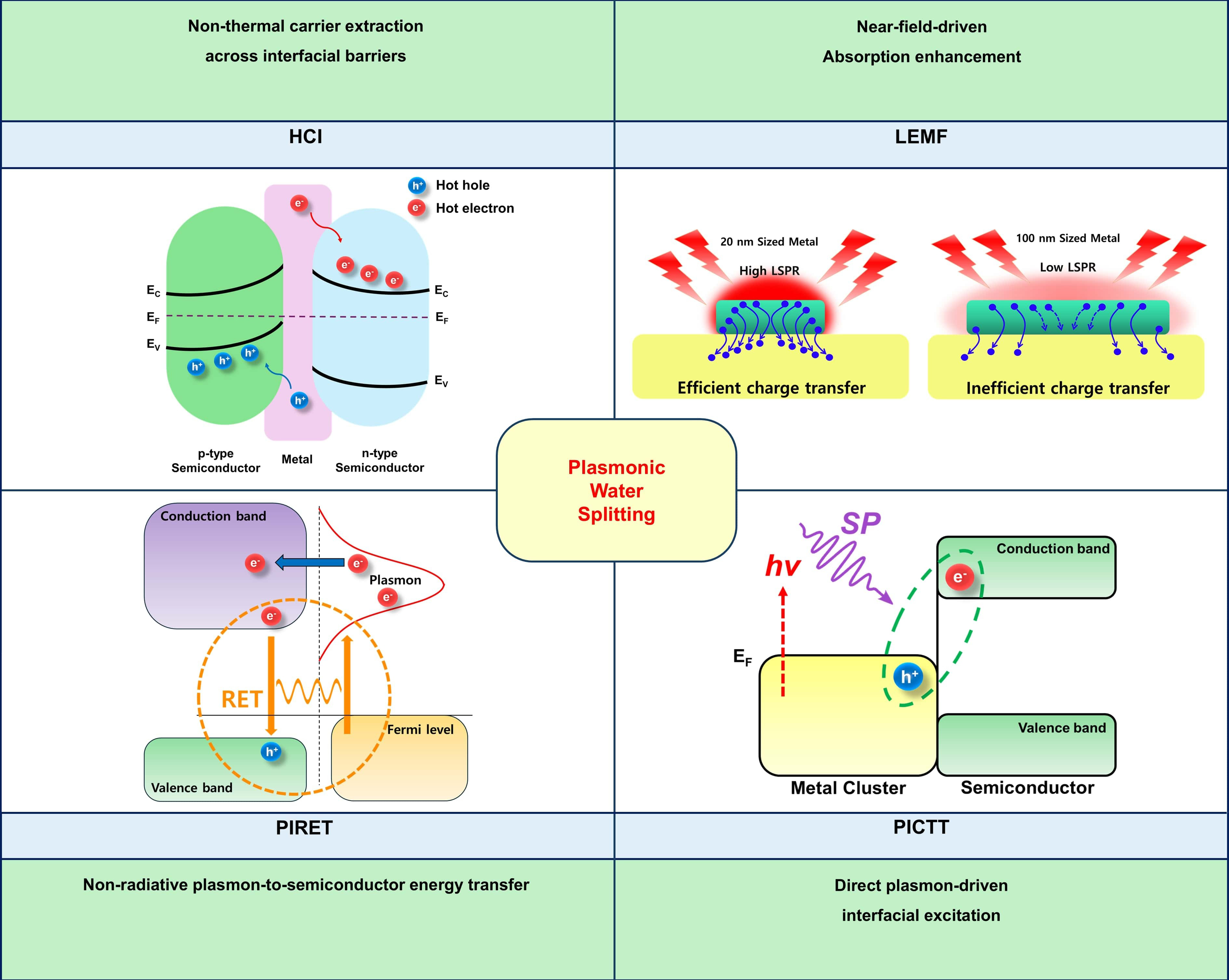
Figure 4. Schematic illustration of plasmonic mechanisms in photoelectrochemical water splitting. The upper left panel illustrates HCI, where non-thermal electrons and holes generated by plasmon decay traverse interfacial energy barriers[87]. Copyright 2025, reproduced with permission. Published by American Chemical Society. The upper right panel depicts LEMF, in which near-field concentration around plasmonic nanostructures amplifies optical absorption and charge generation in the adjacent semiconductor[144]. Copyright 2021, reproduced with permission. Published by American Chemical Society. The lower left panel shows PIRET, a non-radiative process that transfers plasmon energy to semiconductor excitations without direct carrier injection[123]. Copyright 2012, reproduced with permission. Published by American Chemical Society. The lower right panel represents PICTT, where plasmon excitation directly drives electronic transitions across the metal-semiconductor interface[88]. Copyright 2019, reproduced with permission. Published by American Chemical Society. HCI: Hot carrier injection; PIRET: plasmon-induced resonant energy transfer; LEMF: localized electromagnetic field enhancement; PICTT: plasmon-induced metal-to-semiconductor interfacial charge-transfer transition; LSPR: localized surface plasmon resonance; SP: surface plasmon; EC: conduction band edge; EF: Fermi Leve; EV: valance band edge.


