


fig6
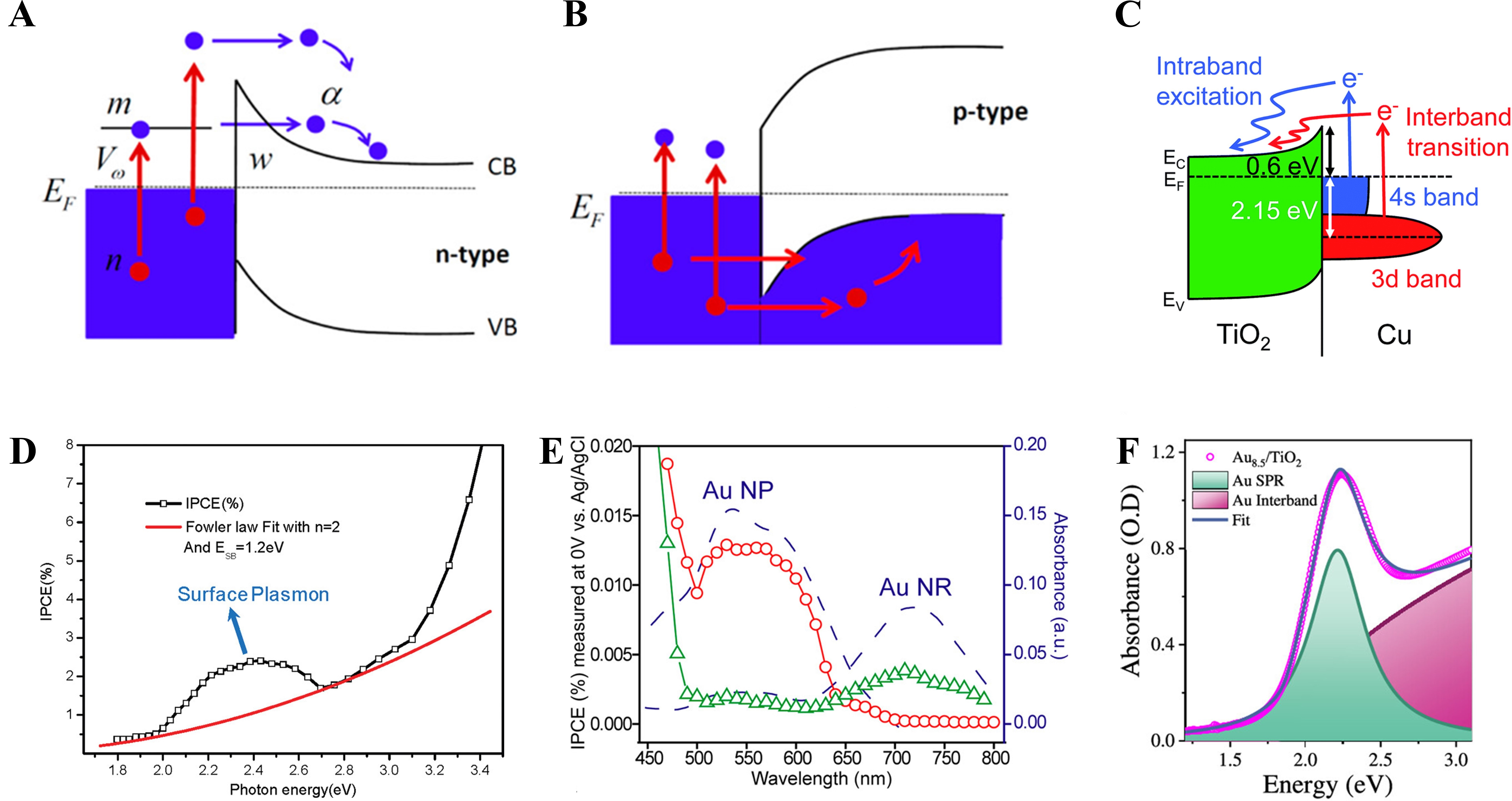
Figure 6. Mechanisms of Plasmon-Induced HCI and Resulting IPCE Enhancement in Metal-Semiconductor. (A) n-type semiconductor junction; (B) p-type semiconductor junction[97]. Copyright 2013, reproduced with permission. Published by the American Chemical Society; (C) Band alignment of Cu/TiO2, emphasizing band excitation processes[60]. Copyright 2019, published by the Royal Society of Chemistry; (D) IPCE-photon energy dependence with surface plasmon enhancement region and Fowler law fitting[105]. Copyright 2011, published by the American Chemical Society; (E) Wavelength-resolved IPCE and absorption spectra of Au nanoparticles and Au nanorods[106]. Copyright 2013 American Chemical Society; (F) Absorption spectrum decomposition of Au/TiO2 into LSPR and interband contributions[107]. Copyright 2025 American Chemical Society. CB: Conduction band; EC: conduction band edge; EF: Fermi Leve; EV: valance band edge; VB: valance band; IPCE: incident photon-to-current efficiency; NP: nano-particle; NR: nano-rod; LSPR: localized surface plasmon resonance.


