


Preparation and research progress of GaN-based avalanche photodetectors


Abstract
The demand for single-photon high-sensitivity ultraviolet (UV) detection is continuously increasing in cutting-edge fields such as UV astronomy, environmental monitoring, and space communications. In particular, gallium nitride (GaN) is an ideal material for UV detection due to its wide bandgap (3.4 eV), strong radiation immunity, and visible/solar-blind properties. In this respect, avalanche photodetectors (APDs) are very promising candidates for single-photon UV detection due to their high sensitivity, large gain, high detection efficiency, and room temperature operation. This review summarizes the GaN avalanche breakdown characteristics, including current surge, positive temperature coefficient of Vbr, and non-linear characterization. In addition, recent advances in various structural types of GaN APDs, such as p-i-n, separated absorption multiplication, optimized edge termination, and polarization-enhanced structures, are presented. In addition, the directions and challenges for the future development of GaN APDs are discussed. Although GaN-based APDs have significantly improved their UV single-photon detection performance through structural innovations, noise control, linearity optimization, and process simplification remain the core challenges. In the future, the integration with two-dimensional material heterojunction and new light trapping structure is expected to break through the existing bottleneck and promote its application in frontier fields such as deep space exploration and quantum communication.

Keywords
INTRODUCTION
In 1801, Johann Ritter first discovered ultraviolet (UV) light in solar radiation[1]. Moderate amounts of UV radiation are beneficial to human health, but excessive UV exposure may cause a variety of negative effects, including skin damage, reduced crop yields, and accelerated aging of buildings[2,3]. Therefore, monitoring of UV rays in the environment is essential. A photodetector converts an optical signal into an electrical signal, and its response spectral range depends on the bandgap of the semiconductor material. With the sharp increase in the demand for single-photon level high-sensitivity UV detection in cutting-edge fields such as UV astronomy, environmental monitoring, and space communications[4-6], there are stringent requirements for the sensitivity of UV detectors. At present, weak UV detection is mainly achieved through photomultiplier tubes[7-9]. However, there are some shortcomings, including high cost, short lifetime, fragility, low quantum efficiency, and high operating voltage[9]. Compared with photomultiplier tubes, avalanche photodetectors (APDs) have the advantages of high sensitivity, large gain, and high detection efficiency, thus being a strong candidate for single-photon UV detection. Moreover, it has the potential to overcome many limitations of photomultiplier tubes, bringing new opportunities to UV detection in cutting-edge fields like UV astronomy, environmental monitoring, and space communications.
Photodetectors can be roughly categorized into photodiodes (PDs) without internal multiplication and PDs with internal multiplication; the former include general PDs, p-i-n tubes, photoconductive detectors, and metal-semiconductor-metal (MSM) PDs, and significant progress has been made[10]; the latter encompass APDs and field-effect phototransistors (FEPTs). APD is a highly sensitive photodetector with internal amplification that uses the avalanche multiplication effect to significantly increase the intensity of the photoelectric signal, enabling it to detect extremely weak light features, even single photons. Figure 1A illustrates the collisional ionization process of electrons in p-i-n structures when light is illuminated on p-GaN. When the energy of a photon hitting the light-sensitive surface of the detector is greater than the bandgap of the material of the detector, i.e., when ħν > Eg, the photon is absorbed while an electron-hole pair is generated. In the depletion region, the photogenerated carriers (holes and electrons) are separated and accelerated by a powerful electric field (EF). Once they acquire sufficiently large kinetic energy, these carriers collide with the lattice atoms, causing ionization and generating secondary electron-hole pairs. These pairs are accelerated and continue to produce more electron-hole pairs, causing an electron multiplication avalanche. A typical gain (M)-voltage (V) curve of APD is depicted in Figure 1B. The APD can work in both linear and Geiger modes. When the bias voltage is higher than the Vbr, i.e., the APD is operating in Geiger mode, the avalanche gain is high, and weak signals and even single photons can be detected. Geiger APDs, also known as single-photon avalanche photodiodes (SPADs), are widely used in quantum communications[11-13], astronomical observations[14,15], and medical imaging[16-18].

Figure 1. (A) Collisional ionization of electrons in p-i-n structure; (B) a typical gain-voltage curve of an APD. p-i-n: Positive-intrinsic-negative; APD: avalanche photodetector.
Si-based APDs are the most common commercial representors of UV SPAD due to the process maturity, compatibility with complementary metal oxide semiconductor (CMOS) processes, and low noise[19-21]. Recently, Si-based APDs have demonstrated an UV responsivity of 6.79-14.51 A/W with wavelengths in the range of 300-400 nm at a reverse bias voltage of 20.02 V[21]. However, Si photosensors have inherent drawbacks, such as low UV efficiency and narrow bandgap (1.12 eV), resulting in an untunable spectral response from the near-UV to the near-IR range, which must be limited by optical filters[22]. In contrast, the gallium nitride (GaN) semiconductor material has a bandgap of 3.4 eV, exhibiting effective UV absorption[23,24]. It is also characterized by good thermal conductivity[25], high critical electric field strength[26], and high electron saturation drift rate[27], making it more suitable for UV detection in extreme environments[28]. GaN-based APDs have attracted much attention because of their visible blindness or solar blindness, strong radiation resistance, and other advantages. Therefore, analyzing and investigating GaN-based APDs is important to promote scientific progress in cutting-edge fields, especially in enhancing the performance of high-sensitivity UV optoelectronic devices.
This review focuses on GaN-based avalanche photodetectors for UV single-photon detection. First, the main performance parameters of GaN APDs and GaN avalanche breakdown characteristics are introduced [Figure 2]. Then, the research progress of GaN-based avalanche photodetectors is discussed from the structural point of view, including p-i-n APDs, separated absorption multiplication (SAM)-type APDs, optimized edge-terminations APDs, and polarization-enhanced APDs. Finally, two major directions for future GaN-based avalanche photodetectors, namely plasmon combination and integration of 2D materials, are proposed.

Figure 2. The avalanche breakdown characteristic, structure section, and some examples of avalanche photodetectors. Vbr: Breakdown voltage; GaN: gallium nitride; p-i-n: positive-intrinsic-negative; APD: avalanche photodetector; SAM: separated absorption multiplication.
THE MAIN PERFORMANCE PARAMETERS OF GaN APDs
Breakdown voltage
Breakdown voltage (Vbr) of APDs is the critical voltage value at which the avalanche breakdown phenomenon occurs in the device under reverse bias. At this point, the current increases dramatically and the gain tends to infinity, but in practice, there is a limited maximum gain due to material defects or structural limitations. In practice, APDs are usually operated at a voltage slightly lower than Vbr to avoid excessive noise and possible risk of breakdown while obtaining sufficient gain. Vbr can be mathematically written as follows:
where εc is the material critical electric field strength and Wd is the depletion layer width.
External quantum efficiency
External quantum efficiency (η) is the main performance index of APDs. It is defined as the ratio of the number of electron-hole pairs produced per second to the number of photons incident per second, thus reflecting the conversion efficiency between the input optical signal and the output electrical signal. η is related to the optical absorption coefficient (α0) and the thickness of the optical absorption layer (W), and it can be mathematically written as follows:
where Ilight is the current under light, q is the elementary charge, h is the Planck constant, ν is the optical frequency, and Popt is the optical power.
Dark current
The dark current (Idark) is the current in the absence of light irradiation and reflects the noise level of the UV detector. The dark current mainly comes from carrier generation-complex current in the depletion layer, minority carrier diffusion current, and surface leakage current. Compound and diffusion currents can be effectively suppressed by reducing the defect density of the material, and surface leakage currents can be reduced by passivating the surface, thus optimizing device performance.
Responsivity
Responsivity (R) is a physical quantity that describes the photovoltaic conversion capability of a device, defined as the ratio of the photocurrent generated by the external circuit to the incident optical power. R can be mathematically written as follows:
where Iph is the photocurrent.
Multiplication factor
The multiplication factor (Mn) is a key parameter characterizing the amplification capability of the device and is defined as the ratio of the photocurrent at the avalanche voltage to the photocurrent at the reference bias (Vgain=1). Mn can be mathematically written as follows:
CHARACTERISTICS OF GAN AVALANCHE BREAKDOWN
The current surges
When the voltage reaches the breakdown voltage of the device, the current rises sharply, and Figure 3A illustrates the current-voltage (I-V) curve. The dark current of GaN APDs stays low at reverse voltages of 0-Va, but rises exponentially with the increase in reverse bias voltage when the reverse voltage is greater than premature breakdown voltage (Va). This is due to the thinning of the p-i-n barrier under an applied electric field, as depicted in Figure 3B, which allows electrons or holes to pass through the “wall” that they would otherwise be unable to cross, promoting defect-assisted tunneling and interband tunneling. Tunneling is associated with material defects that create deep energy levels within the bandgap, and the increase in the density of these levels enhances the probability of tunneling[29]. When the reverse bias voltage exceeds the breakdown voltage (Vbr), the collisional ionization of electrons and holes occurs in the multiplication region. As a result, the dark current surges and collisional ionization begins to dominate the current, producing the avalanche gain. Notably, when the voltage continues to increase, the avalanche gain does not just increase, but decreases slightly[30]. This is because the photocurrent is saturated under the action of the electric field, while the dark current as being mainly related to various processes (trap-assisted tunneling, band-band tunneling, generation-recombination current, and surface leakage current[30,31]) will increase to a small extent with the increase in voltage, leading to a slight decrease in the gain. Therefore, it is necessary to reduce the material defect density to prevent premature breakdown[32].
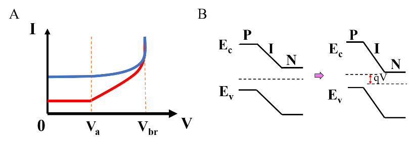
Figure 3. (A) I-V curves of GaN APDs under dark and light conditions; (B) energy band diagrams change after pressurization. I-V: Current-voltage; Vbr: breakdown voltage; GaN: gallium nitride; APD: avalanche photodetector.
Positive temperature coefficient of Vbr
The most significant feature of GaN APDs avalanche breakdown is the positive temperature coefficient of the Vbr[33,34], which is about 0.023 V/K. The temperature-dependent Vbr can be mathematically written as follows:
where α denotes the temperature coefficient.
At high temperatures, the carrier energy loss due to lattice scattering is greater than that at low temperatures, and the carriers require a larger bias voltage to obtain sufficient collisional ionization energy. Thus, the temperature dependence of the Vbr can be used to confirm whether the gain comes from the avalanche multiplication process. When the α of the Vbr is positive, it indicates that the gain of the APDs is caused by the avalanche collisional ionization rather than other mechanisms (e.g., Zener tunneling, defect-assisted tunneling, and premature breakdown), which is because of the leakage from the microplasma or the sidewalls of the mesa, which are all temperature-insensitive processes[35]. On the other hand, the photoconductor gain increases linearly with the bias voltage and can also be excluded from the internal gain mechanism[36]. Moreover, it was discovered that the value of α in AlGaN SAM APDs is almost twice as high as the value in AlGaN p-i-n APDs, achieving a level of up to 0.05 V/K[37,38]. This is because the avalanche process in SAM-APDs mainly originates from holes to initiate collisional ionization, while in p-i-n-type APDs, it originates from both holes and electrons to initiate collisional ionization. Meanwhile, the hole collisional ionization coefficient β is more temperature-dependent than the electron collisional ionization coefficient[39]. Jeong et al. investigated the breakdown voltage temperature coefficients with and without ion implantation and found that the average value in AlGaN APDs without ion implantation was -0.069 ± 0.009 V/K, while being -0.052 ± 0.005 V/K in devices with ion implantation. Therefore, the temperature coefficients of ion-implanted APDs are increased by ~ 25% relative to those of APDs without ion implantation. However, all these coefficients are negative, requiring an in-depth analysis of the underlying physical mechanisms[40].
Non-linear characterization
Linearity is one of the most important indicators of the performance of APDs, which directly affects the accuracy of the APD output signal. The non-linear phenomenon in GaN APDs is manifested as a decrease in internal gain with increasing optical input power[41], as shown in Figure 4A, which reduces the optical response. As soon as the internal current reaches saturation, numerous carriers accumulate at the depletion layer when high optical power is input, forming space charges [ Figure 4B and C]. These space charges generated by high optical power neutralize the charges in the depletion layer, which leads to a decrease in the electric field strength and the collisional ionization rate in the multiplication region [Figure 4D]. However, the actual APD structure will exhibit a lower linearity than the ideal structure, which requires the appropriate theoretical analysis for the in-depth exploration of more complex cases.

Figure 4. (A) Gain and bias curves at different optical input powers; energy band diagrams of GaN SAM APDs at (B) low and (C) high optical inputs; (D) electric field distributions in different regions of GaN SAM APDs at different optical input powers[41]. GaN: Gallium nitride; SAM: separated absorption multiplication; APD: avalanche photodetector.
ADVANCES IN GaN-BASED AVALANCHE PHOTODETECTORS
Recent advances in GaN APDs are discussed below in terms of different structural designs, including p-i-n-type APDs, SAM-type APDs, optimized edge termination APDs, and polarization-enhanced APDs.
P-i-n APDs
Since Osinsky et al. initially discovered the avalanche process in GaN-based p-i-n photodiodes in 1998[42], numerous research teams have profoundly investigated and explored the structure and physical mechanism of GaN-based APDs so as to improve their performance. Early GaN p-i-n APDs were based on GaN grown on sapphire, as shown in Figure 5A[43-45]. Nevertheless, the significant lattice mismatch between the GaN layer and the sapphire substrate resulted in high dark current density. With the commercialization of high-quality bulk GaN substrates, GaN p-i-n APDs grown on bulk GaN substrates have been rapidly developed

Figure 5. (A) Schematic structure of GaN p-i-n APDs grown on sapphire substrates; (B) schematic structure of GaN p-i-n APDs grown on bulk GaN substrates; (C) schematic structure of Al0.05Ga0.95N p-i-n APDs with step gradients; (D) schematic structure of back-illuminated p-i-n APDs on sapphire substrates; (E) schematic structure of front-illuminated n-i-p APDs on block GaN substrate; (F) schematic structure of GaN-based APDs with SAM structure; (G) schematic structure of front-illuminated GaN p-i-p-i-n APDs with a thin AlGaN window layer. GaN: Gallium nitride; p-i-n: positive-intrinsic-negative; APD: avalanche photodetector; SAM: separated absorption multiplication.
It was found that the collisional ionization coefficient of holes in GaN is much larger than that of electrons, whereas the noise contribution from the electron injection is higher; therefore, the lower excess noise factor and the higher gain can be achieved by using holes to initiate avalanches[59-62]. K is defined as the ratio of the hole ionization coefficient β to the electron ionization coefficient α, i.e., K = β/α. For the AlxGa1-xN material, the value of K is greater than 1 when x < 0.5, which means that the use of hole-induced collisional ionization is more effective and higher gain can be obtained; when x > 0.6, the value of K is less than 1, which indicates that collisional ionization using electrons to go is more effective. Therefore, to obtain the higher gain, the low-Al component AlGaN with a higher collisional ionization coefficient and lower dislocation density usually serves as the multiplier layer[63,64]. To effectively utilize holes and initiate the multiplication process in GaN APDs, it is necessary to transform n-GaN into the light-receiving surface, because the built-in electric field of the PN junction is pointing from N to P. When hitting n-GaN, the UV photon will be absorbed, and the resulting electron-hole pairs will be separated under the action of the built-in electric field, while the hole will be accelerated until the collisional ionization. As a result, the backside-illuminated GaN p-i-n APDs on UV-transmitting sapphire and the frontside-illuminated GaN n-i-p APDs on bulk GaN substrates have been proposed[59,65-67]. The schematics of the corresponding light-illuminated devices are displayed in Figure 5D and 5E, among which the structure on n-GaN utilizes holes to initiate multiplication. Ji et al. prepared GaN n-i-p APDs on freestanding GaN substrates with the photoresponsivity of 60 A/W, the greatest responsivity of any GaN APD yet documented. The gain was as high as 105 at 280 V reverse bias voltage with a dark current density of 1.5 × 10⁻⁵ A/cm2[67].
Notably, substrate choice has a significant impact on the performance and manufacturing cost of GaN APDs. Si substrates have the lowest cost, but have high lattice mismatch (~ 17%) and require a buffer layer to mitigate the lattice mismatch, leading to higher defect densities; sapphire substrates are moderately expensive and support backside irradiation, but have the same high lattice mismatch (~ 16%), leading to higher defect densities; SiC substrates have good thermal conductivity and small lattice mismatch (~ 3.5%), but are more expensive; high-quality lumped gallium nitride substrates can lower the defect density; however, they are extremely expensive due to the current challenges in manufacturing. GaN APDs grown on SiC/bulk-GaN substrates are suitable for high-end scenarios (deep space exploration, etc.), while GaN APDs grown on sapphire/Si substrates are suitable for civilian applications.
SAM APDs
The SAM structure can reduce the noise and improve the avalanche gain during collisional ionization[68]. This is due to the insertion of a charge layer between the absorber layer and the multiplication layer of the GaN APDs, which can greatly prevent electrons from entering the multiplication layer, thus realizing only hole-initiated multiplication. The noise sources affecting the detection sensitivity of the APD itself come from the photoelectric effect and avalanche gain process. Among them, the random ups and downs of the gain owing to the photogenerated carrier multiplication produce a noise level that exceeds the original level where only the bulk noise is amplified, which is called the excess noise. Since the excess noise strongly depends on the ratio of hole to electron dissociation rates K (or the ratio of electron to hole dissociation rates K’), the excess noise factor Fh (M0) at the moment of only the hole injection can be mathematically written as follows[69]:
where K’ = α/β, and M0 = < M0> denotes the average gain.
To obtain a low excess noise factor, K’ must be minimized. The SAM structure allows for nearly pure hole doubling with a very small K’, resulting in low noise and increased gain. The structure of the respective GaN SAM APD is depicted in Figure 5F[38,70]. The SAM structure reduces noise and boosts gain by isolating the absorption and multiplication regions through a charge layer, but the increased process complexity could lead to higher costs. However, its performance benefits in high gain-bandwidth product scenarios (e.g., 5G communications) can offset the additional cost and create a competitive differentiator. Since the surface of the material also absorbs the incident light, when the depletion layer does not reach the surface, the electrons and holes will not be able to separate and complex quickly enough to collect the electrons. η value is related to the ability to collect incident photons, so this is the key issue that leads to the low η of the device. To address the problem, Ji et al.[71] prepared a front-illuminated GaN p-i-p-i-n APD with a thin AlGaN window layer. The respective structure is depicted in Figure 5G. The p-Al0.05Ga0.95N layer can transmit the equivalent UV light due to its greater bandgap than GaN. This reduces incident light absorption at the material surface and improves the η and responsivity. The avalanche breakdown occurred at a reverse bias greater than 72.5 V, achieving a high avalanche gain higher than 8.0 × 10⁵[71].
Microplasma breakdown (MPB), a form of p-n junction reverse localized avalanche breakdown, has been recognized in past studies as a negative factor that degrades device performance. However, if MPB can be reproduced artificially, it will show great potential application value. Cao et al. observed a unique microplasma breakdown behavior in AlGaN-based p-i-n-i-n APDs, realizing an avalanche gain as high as 3 × 10⁶ and a light-to-dark current ratio of more than 107 at a breakdown voltage of 107 V[72]. According to the characteristics of MPB, it is expected that high photoelectric gain with low dark current background can be achieved via the localized avalanche breakdown in microplasma. In this respect, many methods have been proposed to optimize the edge termination and enhance the polarization based on the SAM structure so as to reduce the operating voltage of the photodetector device, increase the polarization strength, and reduce the leakage current, which will be discussed in detail later.
Optimized edge termination APDs
Properly designing the EF distribution is crucial to realizing robust avalanche breakdown and further reducing surface leakage current[73,74]. Devices with dense EF lines at the edges are prone to premature breakdown, causing an increase in dark current. Edge termination (ET) can terminate the electric field lines at the device edge, thereby reducing the localized peak electric field and preventing premature breakdown. Edge terminations include ion implantation[33,61,62,67,75-78], field plates[73], beveled mesa[79-81], deep vertical mesa[52,82], and mesa passivation[83,84], and the corresponding structures are schematically shown in Figure 6.

Figure 6. (A) Schematic structure of ion implantation ET; (B) schematic structure of field plates ET; (C) schematic structure of beveled mesa ET; (D) schematic structure of deep vertical mesa ET; (E) schematic structure of double mesa ET; (F) schematic structure of mesa passivation ET. ET: edge termination.
Mesa ET, including vertical mesa, double mesa, triple mesa, and beveled mesa structures, has become one of the most popular mesa ET strategies because of the ease of preparation of mesa ET. However, since the dry etching employed to form the device mesa during fabrication can lead to surface defects, increasing leakage current and causing premature device breakdown (microplasma breakdown), Zhang et al. previously prepared a GaN p-i-n APD on bulk GaN via “ledged” surface depletion technique to avoid the aforementioned issues[49]. Later, Nomoto et al. compared five different configurations of GaN PDs: no field-plate (NFP), spin-on-glass passivated with no field-plate (SOG-NFP), long field-plate (LFP), and beveled-mesa with and without field-plate[74]. GaN PDs with LFP structures were found to achieve higher breakdown voltages ranging from 1 kV to 3 kV than GaN PDs without LFP structures. Moreover, the breakdown voltage of GaN PDs with both LFP and beveled-mesa structures is further increased to 3.2 kV. Therefore, the use of a long field plate and beveled countertop can significantly improve the uniformity of device performance and increase the breakdown voltage. Later, Wang et al. produced a GaN APD with a beveled mesa surface of 12° to achieve uniform avalanche breakdown and reduced dark current[85]. However, the dark current mechanism has not been investigated in detail by Wang et al.[85] The angle of the mesa can be further reduced to explore the most suitable angle. Recently, Xu et al. prepared a GaN p-i-n APD grown on bulk GaN substrates with a 1.8° beveled countertop[80], and simulated GaN p-i-n APDs with beveled table angles of 85°, 45°, 5°, and 1.8° with TCAD, and found that the EF distribution is inhomogeneous when the mesa inclination angle is 85°. The peak of EF appears at the bottom of the sidewalls of the mesa, whereby the edge termination is located in the depletion region. With the drop in the inclined mesa angle, the crowding of the local field decreases and moves away from the edge of the device mesa. Therefore, this uniform electric field distribution enables the design and fabrication of the shallow stage edge termination, which effectively eliminates the premature breakdown of GaN-based UV APD devices and reduces the dark leakage current density.
However, achieving avalanche breakdown in GaN APDs through mesa isolation imposes high demands on the fabrication process. Additional designs, such as field plates, may also be required[73]. In addition, mesa etching may damage the surface[86], causing an increase in device leakage current. Therefore, it is necessary to investigate new ET methods. ET using hydrogen plasma (HP) is another easy-to-prepare ET method, where HP is employed to transform the GaN surface into highly resistive GaN[87-89]. Fu et al. proposed the use of hydrogen plasma for surface processing, which combines mesa-ET and HP (MHP-ET) to prevent premature breakdown[90]. GaN p-i-n APDs grown on bulk GaN substrates based on mesa-ET and MHP-ET were prepared and compared, and the respective device structures are depicted in Figure 7A. As can be seen from Figure 7B, destructive breakdown occurs at about 450 V for mesa-ET devices, while non-destructive avalanche breakdown occurs at about 470 V for MHP-ET devices. This is because MHP-EF mitigates the EF distribution on the device surface and reduces the EF value, thus avoiding premature damaging breakdown. In addition to treating the device surface with hydrogen plasma, Zheng et al. also proposed to use plasma containing CHF3, which is also helpful in reducing the dark current[91]. Besides the above methods, various approaches have been introduced to optimize the GaN APDs edge terminations. Cho et al. transformed the injection region into an insulating material by applying a series of N ion injection energies and dosages to achieve effective device isolation and floating guard ring (FGR) formation[92].

Figure 7. (A) Schematic structure of GaN p-i-n APDs grown on bulk GaN substrates based on Mesa-ET (left) and MHP-ET (right); (B) I-V characteristics of GaN p-i-n APDs grown on bulk GaN substrates based on Mesa-ET (left) and MHP-ET (right)[90]. GaN: gallium nitride; p-i-n: positive-intrinsic-negative; APD: avalanche photodetector; ET: edge termination; MHP-ET: I-V: current-voltage.
As for AlGaN APDs, the lack of natural substrates for AlGaN leads to a high defect density and high leakage currents[93]. To realize high-performance AlGaN APDs, You et al. improved the sidewall morphology and sufficiently suppressed the dark current through KOH surface treatment and SiO2 passivation, and finally achieved a gain of more than 2 × 10⁶ and a responsivity of 0.037 A/W without premature breakdown[83]. However, it was subsequently found that ion sputtering during the plasma enhancd chemical vapor deposition passivation process produces plasma damage concentrated in the sidewall[94,95]. Therefore, a two-step deposition method was used, with a low RF power of 20 W in the initial stage and an optimal radio frequency (RF) power of 50 W in the next stage, reducing the damage caused by passivation[84]. This enabled the optimization of vertical-mesa Al0.1Ga0.9N p-i-n APDs based on sapphire substrates by surface treatment and low-damage passivation methods to decrease surface leakage current and achieve robust avalanche breakdown. Meanwhile, because of the lack of suitable edge termination, the peak electric field remained concentrated at the periphery of the device, and high-performance Al0.1Ga0.9N p-i-n APDs were produced via a negative beveled edge termination technique[79]. By optimizing the photoresist reflow and inductively coupled plasma (ICP) etching processes, an ultra-low slope angle of 2 degrees was achieved. The device has a stable breakdown voltage of around 115.9 V, a low dark current density below 5 × 10⁻⁴ A/cm2, and a high avalanche gain of more than 7 × 10⁶. In addition, the beveled edge termination improves the surface loss to UV absorption and ensures a high η of 29.74% at zero bias. Recently, Cao et al. also prepared Al0.lGa0.9N APDs with a 2-degree ultra-low-slope angle[96]. The devices were found to have temperature-dependent low-frequency noise characteristics.
Many other methods that can optimize the edge termination of AlGaN APDs have been proposed as well. Jeong et al. prepared an Al0.6Ga0.4N p-i-n APDs on bulk AlN and compared the performance of APDs with and without ion implantation[40]. It was found that the dark current density of the device using the ion implantation method was reduced from 1 × 10⁻⁸ A/cm2 to 1 × 10⁻⁹ A/cm2, the optical gain increased from 2.43 × 10⁴ to 5.2 × 10⁵, and the device performance was improved to be able to operate at higher current densities without damaging the device [40].
Polarization-enhanced APDs
To detect weak signals or even single photons, APDs need to operate in Geiger mode, i.e., GaN APDs need to operate at voltages greater than 100 V. However, higher operating voltages can cause the electric field to accumulate too much on the surface, leading to premature damage[97]. So, to improve the device’s performance, the breakdown voltage should be minimized. It is known from Equation 1 that the breakdown voltage is related to εc and Wd, and the polarization effect can effectively reduce Wd and provide part of the electric field to maintain εc, thus reducing the breakdown voltage. The specific mechanism is as follows: in group III nitride (e.g., GaN/AlGaN) heterojunctions, spontaneous polarization and piezoelectric polarization are superimposed to form a strong built-in electric field. The polarization field acts synergistically with the applied reverse bias to concentrate the high electric field region near the narrow heterojunction interface (e.g., the AlGaN/GaN interface) instead of uniformly distributing it throughout the depletion layer as in conventional APDs. The polarization field compresses the E-field energy of the applied bias voltage into a smaller spatial area, significantly increasing the local E-field strength and thus triggering avalanche breakdown at lower applied voltages. Therefore, many attempts have been made to improve the polarization strength, e.g., via adjusting the GaN APDs structure design, optimizing the doping concentration in the composition gradient layer, and introducing an AlGaN interlayer into the APDs[30,32,64,98-100]. Meanwhile, even though GaN APDs with the AlGaN layer demonstrate a higher avalanche gain, their operating voltage also increases. In addition, the lattice mismatch between AlGaN and GaN is a non-negligible problem with the increase of the Al content.
To date, a great variety of methods have been proposed to improve the polarization strength by increasing the doping concentration of p-GaN. However, Mg as the dopant is subjected to the higher primary activation energy and its p-type doping efficiency is relatively low. When the doping concentration in p-GaN increases, it affects the performance of the device[101]. Wang et al. simulated and analyzed an alternative doping system using a p-In0.05Ga0.95N layer to replace the p-GaN system in a GaN-based p-i-n APD, and the corresponding structure is displayed in Figure 8A[32]. Due to the lower activation energy of magnesium, the p-InGaN layer has a higher hole concentration compared to the p-GaN layer and can enhance the polarization effect at the interface, which reduces the avalanche breakdown voltage. By comparing the electric field distributions of conventional GaN APDs and GaN APDs with p-In0.05Ga0.95N [Figure 8B], it can be found that GaN APDs with p-In0.05Ga0.95N require less working voltage of 101 V to reach the breakdown electric field (3.2 MV/cm) in the multiplication region, while the avalanche Vbr drop can be significantly reduced (by more than 26 V). Introducing new materials to enhance the internal polarization strength is an effective approach that has recently received a great deal of attention. ScGaN is a well-established nitride ferroelectric material with excellent properties[102-104]. Recently, Wang et al. proposed an AlGaN APD with a highly polarized Sc0.05Ga0.95N layer between the absorber and multiplier layers (the respective structure is displayed in Figure 8C)[98]. ScGaN introduces induced polarization between layers, leading to an increase in the interlayer EF, while the internal EF is as high as 2.8 MV/cm, which greatly accelerates the carrier transport. Additionally, the avalanche gain in such a structure (7.2 × 10⁴) is 60% higher than that in the conventional P-i-p-i-n GaN APDs, and the breakdown voltage is reduced to 72 V[98].

Figure 8. (A) Schematic structure of the new p-i-n type GaN-based APDs with p-In0.05Ga0.95N layer replacing the p-GaN layer. (B) Electric field distributions in GaN APDs (left) and GaN APDs with p-In0.05Ga0.95N (right). (C) The SAM structure of the conventional GaN APDs (left) and the SAM structures of the designed ScGaN APDs (right). p-i-n: Positive-intrinsic-negative; GaN: gallium nitride; APD: avalanche photodetector; SAM: separated absorption multiplication.
To enhance the polarization strength in AlGaN APDs, Shao et al. prepared an AlGaN APD consisting of an AlGaN layer with high/low Al content[64]. The conduction band barrier formed by the contact between the Al0.2Ga0.8N layer and the Al0.45Ga0.55N layer can block the passage of electrons, thus reducing the noise of the device. It was found that the breakdown of APDs was much steeper than that of conventional uniform layer-structured APDs, which was attributed to the exponential increase in hole collision ionization coefficients with the decrease in Al content in AlGaN alloys[105]. At the same time, Cai et al. produced an AlGaN SAM APD with the Al content gradient and realized a M of more than 1 × 10⁵ at 92 V. This is attributed to the fact that the polarization can accelerate the holes, as well as the high collisional ionization coefficients of the holes in Al0.2Ga0.8N, which has a low Al content[30]. As shown in Figure 9, the potential barrier generated by the piezoelectric polarization in the conduction band hinders the electron transport into the multiplication region, which decreases the excessive noise and promotes avalanches by pure holes.

Figure 9. Simulated EF distribution (left) and energy band structure (right)[30].PCC: Polarization charge concentration; APD: avalanche photodetector; EF: electric field.
To further regulate the polarized electric field between the double layers, Guo et al. inserted an n-type layer between the doubling regions of the high/low Al content heterostructure [Figure 10A], resulting in a heterostructured AlGaN SAM APDs with a double layer[99]. As shown in Figure 10B, due to the polarization effect, the designed APD has a higher EF for the low aluminum content layer and a lower EF for the high aluminum content layer of the designed APD. This decreases the EF in the absorption region and increases the EF in the multiplication region, which is more favorable for the avalanche process of the SAM APD, where the Vbr decreases from 116.3 V to 96.9 V[99].

Figure 10. (A) Schematic structure of high/low Al content AlGaN SAM sun-blind UV APDs containing the n-type layer; (B) electric field distribution in high/low Al content AlGaN SAM APDs[99]. GaN: Gallium nitride; SAM: separated absorption multiplication; UV: ultraviolet; APD: avalanche photodetector.
OTHER APDS
At present, avalanche photodetectors made of 2D materials with outstanding properties like low surface scattering[106], high atomic layer mobility[107], and tunable bandgap[108] have set off a new research boom. Table 1 summarizes the structures and properties of GaN-based APDs from various reports. Despite the breakthrough in GaN APDs performance[109-112], the current avalanche photodetectors based on the traditional GaN semiconductor material have limitations such as laborious and time-consuming fabrication process, high cost, low responsivity, low quantum efficiency, and high breakdown voltage. In contrast, 2D material avalanche devices exhibit unique physical advantages and process compatibility, which provide a new idea for solving the breakdown voltage-quantum efficiency trade-off dilemma of conventional group III nitride APDs, and also create interface engineering possibilities for the development of mixed-dimensional (2D/3D) heterogeneous integrated devices.
Summary of reported GaN avalanche photodiodes
| Authors | Structures | Substrate | Front/Back illuminated | Electron/Hole initiated | Vbr (V) | η (% before avalanche breakdown) | Idark (A/cm2 at 95% Vbr) | Rmax (A/W) | Gmax |
| AlGaN | GaN | Front | Electron | 100 | 16 | 1 × 10⁻⁴ | 0.8 | ||
| AlGaN | AlN | Front | Electron | 140 | NA | 1 × 10⁻⁵ | 0.7145 | ||
| AlGaN | AlN/ Sapphire | Back | Hole | 92 | NA | 1 × 10⁻⁶ | 0.04 | ||
| AlGaN | AlN/ Sapphire | Back | Hole | 107 | NA | NA | NA | ||
| AlGaN | Sapphire | Back | Hole | 66.5 | NA | 0.04 | 0.15 | ||
| AlGaN | Sapphire | Back | Hole | 90 | NA | 3.5 × 10⁻³ | 2 | ||
| AlGaN | Sapphire | Back | Hole | 80 | NA | 0.8 | NA | ||
| AlGaN | Sapphire | Back | Hole | 96.9 | NA | NA | NA | ||
| AlGaN | Sapphire | Front | Electron | 115.9 | 29.74 | 5 × 10⁻⁴ | 0.8228 | ||
| AlGaN | Sapphire | Front | Electron | 90 | NA | 4.4 × 10⁻⁵ | NA | ||
| Xu et al.[80] | GaN | GaN | Front | Electron | 107 | 74 | 3.4 × 10⁻⁵ | 0.212 | |
| GaN | GaN | Front | Electron | 92.3 | NA | 2 × 10⁻⁴ | 0.15 | ||
| GaN | GaN | Front | Electron | 95.4 | NA | 1 × 10⁻² | 0.14 | ||
| GaN | GaN | Front | Electron | 84 | NA | 1 × 10⁻² | 0.041 | ||
| Ji et al.[67] | GaN | GaN | Front | Hole | 278 | 80 | 1.5 × 10⁻⁵ | 60 | 105 |
| GaN | Sapphire | Back | Hole | 90 | 57 | 0.044 | 0.163 | ||
| GaN | Sapphire | Front | Electron | < 120 | 80.1 | 1.27 × 10⁻⁴ | 0.23 | NA | |
| Verghese et al.[111] | GaN | Sapphire | Front | Electron | 92 | 25-40 | 795 | NA | 300 |
| GaN | SiC | Front | Electron | 160 | NA | 2 × 10⁻⁸ | 4.2 | 105 |
Recently, Gao et al. fabricated a SAM APD based on an Au/WSe2/Ge heterostructure[113]. The respective structure is displayed in Figure 11A. The dark current of the SAM APD is greatly reduced from 1 × 10⁻⁹ A to 2 × 10-11 A. Figure 11B illustrates the I-V curves under different wavelengths of illumination, revealing a clear avalanche multiplication effect. The SAM structures integrated with 2D layered and bulk materials have aroused heated discussion and have a promising development prospect[114-116]. Avalanches arising in 2D materials can be broadly categorized into Schottky-type[113] and van der Waals-type[117-121]. Schottky-type avalanches are typical of the aforementioned Au/WSe2/Ge heterojunction, which is utilized to produce a multiplication effect. In turn, van der Waals-type avalanches can be classified into heterojunction[117,118,120] and homojunction[119,121] 2D material avalanches. In 2019, Gao et al. observed an avalanche breakdown process in an InSe/BP heterostructure with a gain of up to 105 and a dark current of about 100 pA at a voltage of 4.8 V[117]. In 2022, Son et al. fabricated a high-efficiency avalanche photodiode with a WSe2/MoS2 heterostructure based on the two-photon absorption, attaining a gain of about 1300, a responsivity of 88 μA/W, and a dark current of about 100 pA[118]. At the same time, Xia et al. prepared a MoS2 homojunction photodetector and found that various van der Waals materials shifted from n-type doping to p-type due to the change in the number of layers[119]. In 2023, Meng et al. prepared WSe2/WS2 P-N heterostructure devices and observed the avalanche process with a responsivity of 135 A/W[120]. In 2024, Wang et al. reported a low-threshold avalanche effect in the WSe2 stepped structure, where the threshold energy at room temperature was close to the basic limit[121]. Therefore, the selection of appropriate 2D materials and their integration with bulk materials within the GaN SAM APDs will be a promising direction in the future.

Figure 11. (A) Schematic structure of SAM APD based on Au/WSe2/Ge[113]. (B) I-V curves for different wavelengths of illumination[113]. (C) Schematic view (left) and cross-sectional view of the APDs (right)[122]. SAM: separated absorption multiplication; APD: avalanche photodetector; I-V: current-voltage.
In addition to APDs integrated with 2D materials, APDs combined with plasmon have also set off a new research boom. Meanwhile, GaN-based APDs currently suffer from various drawbacks, such as low responsivity and low quantum efficiency, whereby the efficient reflection and absorption of UV light on the GaN surface is a key issue. Recently, Chen et al. designed an APD with a photon-trapping structure, which can increase the QE and reduce the thickness of the absorbing layer of APDs[122]. The corresponding device structure is depicted in Figure 11C. This APD comprises an ultrathin absorber with a sub-micron metal grating array, which is an innovative photon-trapping structure ever demonstrated by researchers. As for GaN films, their high refractive index will partly reflect the incident light, thus affecting the absorption. Therefore, Al plasma with stronger excitation intensity and controllable excitation wavelength is more suitable for GaN. Butun et al. fabricated a GaN PD with Al plasma with a responsivity of 1.7 mA/W, which is eight times that of the plasma-free device[123]. Ahmadivand et al. produced a GaN PD with an array of Al oligomers with a responsivity greater than 21 A/W[124]. Meanwhile, the η of the APD was 8,116%, one hundred times that of the plasma-free device. Dubey et al. prepared a GaN PD with periodic Al nanopore arrays with impressive features (responsivity of 670 A/W, detection rate of 1.48×10¹⁵ Jones, and response time of 51/197 ms)[125]. In addition to these, there are many studies combining plasmon with GaN[126-128]. Therefore, combining plasmons with gallium nitride avalanche photodetectors is a promising direction in the future, which merits further investigations.
SUMMARY AND OUTLOOK
The demand for single-photon level high-sensitivity UV detection in cutting-edge fields such as UV astronomy, environmental monitoring, and space communications continues to skyrocket. APDs are strong candidates for single-photon UV detection due to their high sensitivity, large gain, high detection efficiency, and room-temperature operation. Possessing a direct bandgap of 3.4 eV, GaN materials exhibit a high UV light absorption. Therefore, GaN-based APDs have attracted much attention thanks to visible or solar blindness and strong radiation immunity. This review presents the avalanche breakdown characteristics of GaN, as well as recent advances in p-i-n-type, SAM-type, optimized edge-terminated, and polarization-enhanced structures of GaN APDs. To reduce the surface leakage current, researchers have proposed many solutions, including ion implantation, field plate, slant-cut mesa, deep vertical mesa, and mesa passivation, and the results are remarkable. Moreover, the working voltage is reduced by adjusting GaN APD structure, optimizing the doping concentration of p-type or n-type materials, designing component gradient layers, and introducing AlGaN intermediate layers in the APDs.
However, there are still some bottlenecks to be addressed. In particular, the avalanche multiplication inevitably generates noise, which affects the performance of the detector. In this respect, the SAM structure has been proposed as a solution to reduce the noise. Meanwhile, the sources of the noise and the factors affecting the noise need to be further considered. Moreover, the low linearity of GaN APDs still limits the range of applications. Other challenges are associated with high dark current density, greater than 1 × 10⁻⁶ A/cm2, which call for further exploration of the relevant influencing factors. At the same time, there is low polarization strength, which leads to high breakdown voltage, greater than 66 V. Currently, the fabrication of avalanche photodetectors based on the traditional semiconductor material GaN is a complex and time-consuming process, with substrate costs (e.g., bulk GaN substrates) and Metal-organic Chemical Vapor Depositio equipment costs impeding large-scale production, and ET and polarization enhancement potentially requiring an additional step that raises fabrication costs by at least 10%. In addition, encapsulation technology can limit the use of GaN APDs in real-world production (conventional encapsulation materials tend to absorb UV light and require the development of deep UV transmission windows while maintaining hermeticity). Therefore, it is promising to investigate new structures and incorporate new materials (0D, 1D, 2D materials). In addition to optimized edge termination and enhanced polarization effects, there are two other possible directions for GaN-based avalanche photodetectors: combination with plasma and integration with 2D materials. Combining with plasma can improve the η and response speed, and integrating with 2D materials can lower the avalanche voltage threshold and thus reduce the power consumption.
DECLARATIONS
Authors’ contributions
Made substantial contributions to the conception and design of the study and performed data analysis and interpretation: Lei, Q.
Performed data acquisition, as well as providing administrative, technical, and material support: Li, L.; Lu, W.; Tao, J; Ling, R.
Participation in methodological development, manuscript revision, and critical content review: Zhang, L.; Chen, X.; Wu, S.; Li, S. (Shuwei Li)
Coordinated the entire research process, guided the direction of the writing, and were responsible for finalizing and submitting the manuscript: Li, S. (Shuti Li); Gao, F.
Availability of data and materials
Not applicable.
Financial support and sponsorship
This work was supported by the National Natural Science Foundation of China (Grant Nos. 62375090, 62374062 and 52002135), the National Natural Science Foundation of Guangdong Province of China (Grant Nos. 2023B1515120071, 2022A1515011281, 2021A1515012381 and 2024A1515010409), the Science and Technology Program of Guangdong Province of China (Grant Nos. 2023A0505050131, 2022A0505050066, and 2024A1515011081), the Characteristic Innovation Project of Universities in Guangdong Province (Grant No. 2023KTSCX028), and the Science and Technology Program of Guangzhou, China (Grant Nos. 2024A04J6456 and 202201011803).
Conflicts of interest
All authors declared that there are no conflicts of interest.
Ethical approval and consent to participate
Not applicable.
Consent for publication
Not applicable.
Copyright
© The Author(s) 2025.
REFERENCES
2. Tang, X.; Yang, T.; Yu, D.; Xiong, H.; Zhang, S. Current insights and future perspectives of ultraviolet radiation (UV) exposure: Friends and foes to the skin and beyond the skin. Environ. Int. 2024, 185, 108535.
3. Caldwell, M.; Björn, L.; Bornman, J.; et al. Effects of increased solar ultraviolet radiation on terrestrial ecosystems. J. Photoch. Photobio. B. 1998, 46, 40-52.
4. Maccarone, M. C.; La, R. G.; Catalano, O.; et al. UVscope and its application aboard the ASTRI-Horn telescope. Exp. Astron. 2021, 51, 529-50.
5. Su, L.; Zhou, D.; Lu, H.; Zhang, R.; Zheng, Y. Recent progress of SiC UV single photon counting avalanche photodiodes. J. Semicond. 2019, 40, 121802.
6. Smith, J. P.; Bailey, J. I.; Cuda, A.; Zobrist, N.; Mazin, B. A. MKIDGen3: Energy-resolving, single-photon-counting microwave kinetic inductance detector readout on a radio frequency system-on-chip. Rev. Sci. Instrum. 2024, 95, 114705.
7. Boukhicha, M.; Tsang, T. Y.; Giacomini, G.; Dabiran, A. M.; Cultrera, L. UV hybrid photon detector based on GaN photocathodes and Si low gain avalanche diode. J. Inst. 2024, 19, P07020.
8. Adams, J. H.; Allard, D.; Alldredge, P.; et al. The EUSO-SPB2 fluorescence telescope for the detection of ultra-high energy cosmic rays. Astropart. Phys. 2025, 165, 103046.
10. Su, L.; Zhang, Y.; Xie, J. An all-inorganic CsPbBr3/GaN hetero-structure for a near UV to green band photodetector. J. Mater. Chem. C. 2022, 10, 1349-56.
11. Liu, J.; Jiang, W.; Kumar, S.; Deen, M. J. Time-controlled SPAD receivers in optical wireless communication system. IEEE. Photonics. J. 2023, 15, 1-13.
12. Ribisch, C.; Hofbauer, M.; Kohneh, P. S. S.; et al. Multi-channel gating chip in 0.18 µm high-voltage CMOS for quantum applications. Sensors. (Basel). 2023, 23, 9644.
13. Chen, H.; Chen, X.; Lu, J.; et al. Toward long-distance underwater wireless optical communication based on a high-sensitivity single photon avalanche diode. IEEE. Photonics. J. 2020, 12, 1-10.
14. Hippke, M. Interstellar communication: short pulse duration limits of optical SETI. J. Astrophys. Astron. 2018, 39, 9565.
16. Antolovic, I. M.; Burri, S.; Bruschini, C.; Hoebe, R.; Charbon, E. Nonuniformity analysis of a 65-kpixel CMOS SPAD imager. IEEE. Trans. Electron. Devices. 2016, 63, 57-64.
17. Zhang, Y.; He, Z.; Tong, X.; Garrett, D. C.; Cao, R.; Wang, L. V. Quantum imaging of biological organisms through spatial and polarization entanglement. Sci. Adv. 2024, 10, eadk1495.
18. Van, D. T.; Lapauw, T.; Janssen, S.; et al. 64 × 64 pixel current-assisted photonic sampler image sensor and camera system for real-time fluorescence lifetime imaging. IEEE. Sensors. J. 2024, 24, 23729-37.
19. Liu, Q.; Xu, L.; Jin, Y.; et al. Ultraviolet response in coplanar silicon avalanche photodiodes with CMOS compatibility. Sensors. (Basel). 2022, 22, 3873.
20. Alirezaei, I. S.; Andre, N.; Flandre, D. Enhanced ultraviolet avalanche photodiode with 640-nm-thin silicon body based on SOI technology. IEEE. Trans. Electron. Devices. 2020, 67, 4641-4.
21. Guo, G.; Chen, W.; Zheng, K.; et al. Research on the structure design of silicon avalanche photodiode with near-ultraviolet high responsivity. Photonics 2024, 11, 1.
22. Jimenéz-Vivanco, M. R.; García, G.; Carrillo, J.; et al. Porous Si-SiO2 UV microcavities to modulate the responsivity of a broadband photodetector. Nanomaterials. (Basel). 2020, 10, 222.
23. Li, G.; Zhu, M.; Guo, Z.; et al. Recent advances in III-V nitrides: properties, applications and perspectives. J. Mater. Chem. C. 2024, 12, 12150-78.
24. Chen, K.; Wang, X.; Zou, C.; et al. Two-in-one: end-emitting blue LED and self-powered UV photodetector based on single trapezoidal PIN GaN microwire for ambient light UV monitoring and feedback. Small. Methods. 2023, 7, e2300138.
25. Morkoç, H.; Strite, S.; Gao, G. B.; Lin, M. E.; Sverdlov, B.; Burns, M. Large-band-gap SiC, III-V nitride, and II-VI ZnSe-based semiconductor device technologies. J. Appl. Phys. 1994, 76, 1363-98.
26. Östling, M. High power devices in wide bandgap semiconductors. Sci. China. Inf. Sci. 2011, 54, 1087-93.
27. Chen, X.; Wang, Y.; Jian, J.; Gu, L.; Zhang, Z. Effect of strain on space charge layer in GaN nanowires investigated by in-situ off-axis electron holography. Prog. Nat. Sci:. Mater. Int. 2017, 27, 186-91.
28. Hassan, A.; Savaria, Y.; Sawan, M. GaN Integration technology, an ideal candidate for high-temperature applications: a review. IEEE. Access. 2018, 6, 78790-802.
29. Kozodoy, P.; Keller, S.; Denbaars, S.; Mishra, U. MOVPE growth and characterization of Mg-doped GaN. J. Cryst. Growth. 1998, 195, 265-9.
30. Cai, Q.; Luo, W.; Yuan, R.; et al. Back-illuminated AlGaN heterostructure solar-blind avalanche photodiodes with one-dimensional photonic crystal filter. Opt. Express. 2020, 28, 6027-35.
31. Sun, Z.; Yang, J.; Zhao, D.; et al. Investigation of the leakage mechanism in solar-blind AlGaN p-i-n photodetector at high reverse bias. J. Appl. Phys. 2024, 136, 175701.
32. Wang, H.; You, H.; Pan, D.; et al. Polarization enhanced GaN avalanche photodiodes with p-type In0.05Ga0.95N layer. IEEE. Photonics. J. 2020, 12, 1-6.
33. Kizilyalli, I. C.; Edwards, A. P.; Nie, H.; Disney, D.; Bour, D. High voltage vertical GaN p-n diodes with avalanche capability. IEEE. Trans. Electron. Devices. 2013, 60, 3067-70.
34. Liu, J.; Xiao, M.; Zhang, R.; et al. 1.2-kV vertical GaN fin-JFETs: high-temperature characteristics and avalanche capability. IEEE. Trans. Electron. Devices. 2021, 68, 2025-32.
35. Dyakonova, N.; Dickens, A.; Shur, M. S.; Gaska, R.; Yang, J. W. Temperature dependence of impact ionization in AlGaN-GaN heterostructure field effect transistors. Appl. Phys. Lett. 1998, 72, 2562-4.
36. Tut, T.; Gokkavas, M.; Butun, B.; Butun, S.; Ulker, E.; Ozbay, E. Experimental evaluation of impact ionization coefficients in
37. Sun, L.; Chen, J.; Li, J.; Jiang, H. AlGaN solar-blind avalanche photodiodes with high multiplication gain. Appl. Phys. Lett. 2010, 97, 191103.
38. Huang, Y.; Chen, D. J.; Lu, H.; et al. Back-illuminated separate absorption and multiplication AlGaN solar-blind avalanche photodiodes. Appl. Phys. Lett. 2012, 101, 253516.
39. Massey, D.; David, J.; Rees, G. Temperature dependence of impact ionization in submicrometer silicon devices. IEEE. Trans. Electron. Devices. 2006, 53, 2328-34.
40. Jeong, H.; Cho, M.; Xu, Z.; et al. Ion-implanted Al0.6Ga0.4N deep-ultraviolet avalanche photodiodes. Appl. Phys. Lett. 2023, 123, 121107.
41. Gan, H.; Yu, J.; Wang, X. Enhancing linearity of light response in avalanche photodiodes by suppressing electrode size effect. Sensors. (Basel). 2024, 24, 3366.
42. Osinsky, A.; Shur, M.; Gaska, R.; Chen, Q. Avalanche breakdown and breakdown luminescence in p-π-n GaN diodes. Electron. Lett. 1998, 34, 691-2.
43. Carrano, J. C.; Lambert, D. J. H.; Eiting, C. J.; et al. GaN avalanche photodiodes. Appl. Phys. Lett. 2000, 76, 924-6.
44. Butun, B.; Tut, T.; Ulker, E.; Yelboga, T.; Ozbay, E. High-performance visible-blind GaN-based p-i-n photodetectors. Appl. Phys. Lett. 2008, 92, 033507.
45. Gautam, L.; Lee, J.; Richards, M.; Razeghi, M. Solar-blind deep UV avalanche photodetectors using reduced area epitaxy. IEEE. J. Quantum. Electron. 2023, 59, 1-4.
46. Limb, J. B.; Yoo, D.; Ryou, J. H.; et al. GaN ultraviolet avalanche photodiodes with optical gain greater than 1000 grown on GaN substrates by metal-organic chemical vapor deposition. Appl. Phys. Lett. 2006, 89, 011112.
47. Shyh-chiang, S.; Yun, Z.; Dongwon, Y.; et al. Performance of deep ultraviolet GaN avalanche photodiodes grown by MOCVD. IEEE. Photon. Technol. Lett. 2007, 19, 1744-6.
48. Yoo, D.; Limb, J.; Ryou, J.; et al. AlxGa1-xN ultraviolet avalanche photodiodes grown on GaN substrates. IEEE. Photon. Technol. Lett. 2007, 19, 1313-5.
49. Zhang, Y.; Shen, S.; Kim, H. J.; et al. Low-noise GaN ultraviolet p-i-n photodiodes on GaN substrates. Appl. Phys. Lett. 2009, 94, 221109.
50. Kim, J.; Ji, M.; Detchprohm, T.; et al. Comparison of AlGaN p-i-n ultraviolet avalanche photodiodes grown on free-standing GaN and sapphire substrates. Appl. Phys. Express. 2015, 8, 122202.
51. Li, J.; Gao, J.; Yan, X.; et al. GaN p-i-n ultraviolet photodetectors grown on homogenous GaN bulk substrates. Solid-State. Electronics. 2022, 197, 108419.
52. Fukushima, H.; Usami, S.; Ogura, M.; et al. Deeply and vertically etched butte structure of vertical GaN p-n diode with avalanche capability. Jpn. J. Appl. Phys. 2019, 58, SCCD25.
53. Vashaei, Z.; Cicek, E.; Bayram, C.; Mcclintock, R.; Razeghi, M. GaN avalanche photodiodes grown on m-plane freestanding GaN substrate. Appl. Phys. Lett. 2010, 96, 201908.
54. Gautam, L.; Lee, J.; Brown, G.; Razeghi, M. Low dark current deep UV AlGaN photodetectors on AlN substrate. IEEE. J. Quantum. Electron. 2022, 58, 1-5.
55. Cicek, E.; Vashaei, Z.; Mcclintock, R.; Bayram, C.; Razeghi, M. Geiger-mode operation of ultraviolet avalanche photodiodes grown on sapphire and free-standing GaN substrates. Appl. Phys. Lett. 2010, 96, 261107.
56. Wei, Y.; Xu, W.; Qu, H.; et al. GaN-based low-energy X-ray single photon detector with photon energy resolution and fast response. IEEE. Photon. Technol. Lett. 2024, 36, 123-6.
57. Chen, Y.; Zhang, Z.; Jiang, H.; Li, Z.; Miao, G.; Song, H. The optimized growth of AlN templates for back-illuminated AlGaN-based solar-blind ultraviolet photodetectors by MOCVD. J. Mater. Chem. C. 2018, 6, 4936-42.
58. Kim, J.; Ji, M.; Detchprohm, T.; et al. AlxGa1-xN Ultraviolet avalanche photodiodes with avalanche gain greater than 105. IEEE. Photon. Technol. Lett. 2015, 27, 642-5.
59. Mcclintock, R.; Pau, J. L.; Minder, K.; Bayram, C.; Kung, P.; Razeghi, M. Hole-initiated multiplication in back-illuminated GaN avalanche photodiodes. Appl. Phys. Lett. 2007, 90, 141112.
60. Maeda, T.; Narita, T.; Yamada, S.; et al. Impact ionization coefficients and critical electric field in GaN. J. Appl. Phys. 2021, 129, 185702.
61. Cao, L.; Wang, J.; Harden, G.; et al. Experimental characterization of impact ionization coefficients for electrons and holes in GaN grown on bulk GaN substrates. Appl. Phys. Lett. 2018, 112, 262103.
62. Ji, D.; Ercan, B.; Chowdhury, S. Experimental determination of impact ionization coefficients of electrons and holes in gallium nitride using homojunction structures. Appl. Phys. Lett. 2019, 115, 073503.
63. Jeong, H.; Cho, M.; Xu, Z.; et al. Breakdown characteristics of deep-ultraviolet Al0.6Ga0.4N p-i-n avalanche photodiodes. J. Appl. Phys. 2022, 131, 103102.
64. Shao, Z. G.; Yang, X. F.; You, H. F.; et al. Ionization-enhanced AlGaN heterostructure avalanche photodiodes. IEEE. Electron. Device. Lett. 2017, 38, 485-8.
65. Bayram, C.; Pau, J. L.; Mcclintock, R.; Razeghi, M.; Ulmer, M. P.; Silversmith, D. High quantum efficiency back-illuminated GaN avalanche photodiodes. Appl. Phys. Lett. 2008, 93, 211107.
66. Minder, K.; Pau, J. L.; Mcclintock, R.; et al. Scaling in back-illuminated GaN avalanche photodiodes. Appl. Phys. Lett. 2007, 91, 073513.
67. Ji, D.; Ercan, B.; Benson, G.; Newaz, A. K. M.; Chowdhury, S. 60 A/W high voltage GaN avalanche photodiode demonstrating robust avalanche and high gain up to 525 K. Appl. Phys. Lett. 2020, 116, 211102.
68. Campbell, J.; Dentai, A.; Holden, W.; Kasper, B. High-performance avalanche photodiode with separate absorption ‘grading’ and multiplication regions. Electron. Lett. (UK). 1983, 19, 818-20.
69. Mcintyre, R. Multiplication noise in uniform avalanche diodes. IEEE. Trans. Electron. Devices. 1966, ED-13, 164-8.
70. Zhang, Z.; Sun, L.; Chen, M.; Qiu, X.; Li, B.; Jiang, H. Separate absorption and multiplication AlGaN solar-blind avalanche photodiodes with high-low-doped and heterostructured charge layer. J. Elec. Materi. 2020, 49, 2343-8.
71. Ji, M.; Kim, J.; Detchprohm, T.; Zhu, Y.; Shen, S.; Dupuis, R. D. p-i-p-i-n separate absorption and multiplication ultraviolet avalanche photodiodes. IEEE. Photon. Technol. Lett. 2018, 30, 181-4.
72. Cao, J.; Cai, Q.; You, H.; et al. Observation of photoelectric-induced microplasma avalanche breakdown in AlGaN ultraviolet photodiode with separate absorption and multiplication structure. Appl. Phys. Lett. 2023, 123, 121109.
73. Ohta, H.; Asai, N.; Horikiri, F.; Narita, Y.; Yoshida, T.; Mishima, T. 4.9 kV breakdown voltage vertical GaN p-n junction diodes with high avalanche capability. Jpn. J. Appl. Phys. 2019, 58, SCCD03.
74. Nomoto, K.; Hu, Z.; Song, B.; et al. GaN-on-GaN p-n power diodes with 3.48 kV and 0.95 mΩ-cm2: a record high figure-of-merit of 12.8 GW/cm2. In 2015 IEEE international electron devices meeting, Proceedings of the 2015 IEEE international electron devices meeting (IEDM), Washington, DC, USA, December 7-9, 2015; IEEE Publisher: Piscataway, New Jersey, USA, 2015; pp 9.7.1-9.7.4.
75. Liu, J.; Xiao, M.; Zhang, R.; et al. Trap-mediated avalanche in large-area 1.2 kV vertical GaN p-n diodes. IEEE. Electron. Device. Lett. 2020, 41, 1328-31.
76. Matys, M.; Ishida, T.; Nam, K. P.; et al. Design and demonstration of nearly-ideal edge termination for GaN p-n junction using Mg-implanted field limiting rings. Appl. Phys. Express. 2021, 14, 074002.
77. Matys, M.; Ishida, T.; Nam, K. P.; et al. Mg-implanted bevel edge termination structure for GaN power device applications. Appl. Phys. Lett. 2021, 118, 093502.
78. Duan, Y.; Xie, A.; Fay, P.; et al. 1.7-kV vertical GaN p-n diodes with step-graded ion-implanted edge termination. In 2023 Device Research Conference (DRC), Proceedings of the 2023 Device Research Conference (DRC), Santa Barbara, CA, USA, June 25-28, 2023; IEEE Publisher: Piscataway, New Jersey, USA, 2023; pp 1-2.
79. You, H.; Wang, H.; Luo, W.; et al. High-performance Al0.1Ga0.9N p-i-n ultraviolet avalanche photodiodes with ultra-shallow bevel edge terminations. IEEE. Electron. Device. Lett. 2024, 45, 869-72.
80. Xu, Z.; Detchprohm, T.; Shen, S.; Nepomuk, O. A.; Dupuis, R. D. Low leakage and high gain GaN p-i-n avalanche photodiode with shallow bevel mesa edge termination and recessed window. IEEE. Trans. Electron. Devices. 2024, 71, 3761-8.
81. Shoji, T.; Narita, T.; Nagasato, Y.; et al. Analysis of intrinsic reverse leakage current resulting from band-to-band tunneling in dislocation-free GaN p-n junctions. Appl. Phys. Express. 2021, 14, 114001.
82. Maeda, T.; Narita, T.; Yamada, S.; et al. Impact ionization coefficients in GaN measured by above-and sub-Eg illuminations for p-/n+ junction. In 2019 IEEE international electron devices meeting, Proceedings of the 2019 IEEE international electron devices meeting (IEDM), San Francisco, CA, USA, December 7-11, 2019; IEEE Publisher: Piscataway, New Jersey, USA, 2019; pp 4.2.1-4.2.4.
83. You, H.; Wang, H.; Luo, W.; et al. Al0.1Ga0.9N p-i-n ultraviolet avalanche photodiodes with avalanche gain over 106. IEEE. Electron. Device. Lett. 2022, 43, 1479-82.
84. You, H.; Wang, H.; Luo, W.; et al. Al0.1Ga0.9N p-i-n ultraviolet avalanche photodiodes with suppressed surface leakage current and uniform avalanche breakdown. Opt. Express. 2023, 31, 37516-22.
85. Wang, W. Uniform and high gain GaN p-i-n ultraviolet APDs enabled by beveled-mesa edge termination. IEEE. Photon. Technol. Lett. 2020, 32, 1357-60.
86. Yuhao, Z.; Min, S.; Hiu-yung, W.; et al. Origin and control of OFF-state leakage current in GaN-on-Si vertical diodes. IEEE. Trans. Electron. Devices. 2015, 62, 2155-61.
87. Fu, H.; Fu, K.; Huang, X.; et al. High performance vertical GaN-on-GaN p-n power diodes with hydrogen-plasma-based edge termination. IEEE. Electron. Device. Lett. 2018, 39, 1018-21.
88. Fu, H.; Fu, K.; Liu, H.; et al. Implantation-and etching-free high voltage vertical GaN p-n diodes terminated by plasma-hydrogenated p-GaN: revealing the role of thermal annealing. Appl. Phys. Express. 2019, 12, 051015.
89. Fu, H.; Fu, K.; Alugubelli, S. R.; et al. High voltage vertical GaN p-n diodes with hydrogen-plasma based guard rings. IEEE. Electron. Device. Lett. 2020, 41, 127-30.
90. Fu, K.; He, Z.; Yang, C.; Zhou, J.; Fu, H.; Zhao, Y. GaN-on-GaN p-i-n diodes with avalanche capability enabled by eliminating surface leakage with hydrogen plasma treatment. Appl. Phys. Lett. 2022, 121, 092103.
91. Zheng, B.; Chen, P.; Yu, C.; et al. Suppression of current leakage along mesa surfaces in GaN-based p-i-n diodes. IEEE. Electron. Device. Lett. 2015, 36, 932-4.
92. Cho, M.; Xu, Z.; Bakhtiary-noodeh, M.; et al. 1.2-kV vertical GaN PIN rectifier with Ion-implanted floating guard rings. IEEE. Trans. Electron. Devices. 2023, 70, 4578-83.
93. Wang, W.; Zhang, H.; Li, Q.; Kang, J. Surface smoothing with BCl3 plasma post-treatment to improve the performance of GaN avalanche photodiodes. Jpn. J. Appl. Phys. 2019, 58, 106505.
94. Sheen, M.; Ko, Y.; Kim, D. U.; et al. Highly efficient blue InGaN nanoscale light-emitting diodes. Nature 2022, 608, 56-61.
95. Han, S.; Yang, S.; Sheng, K. High-voltage and High-ION/IOFF vertical GaN-on-GaN schottky barrier diode with nitridation-based termination. IEEE. Electron. Device. Lett. 2018, 39, 572-5.
96. Cao, J.; Wang, H.; You, H.; et al. Temperature dependent low-frequency noise characteristics of AlGaN avalanche photodiodes with ultra-shallow bevel edge termination. J. Alloys. Compd. 2025, 1010, 177934.
97. Bulmer, J.; Suvarna, P.; Leathersich, J.; et al. Visible-blind APD heterostructure design with superior field confinement and low operating voltage. IEEE. Photon. Technol. Lett. 2016, 28, 39-42.
98. Wang, J.; Liang, Y.; Hou, Q.; et al. Polarization enhanced GaN separate absorption and multiplication ultraviolet avalanche photodiodeswith an ScGaN interlayer. Opt. Lett. 2024, 49, 6713-6.
99. Guo, J.; Xie, F.; Gu, Y.; et al. Improved performance of AlGaN solar-blind avalanche photodiodes with dual multiplication layers. Opt. Quant. Electron. 2023, 55, 4400.
100. Sun, Z.; Yang, J.; Zhao, D.; et al. The effect of nanopipes and an inserted n-AlGaN interlayer on GaN avalanche photodiodes performance. Physica. Status. Solidi. (a). 2024, 221, 2300490.
101. Yu, C.; Chu, C. F.; Tsai, J. Y.; Lin, C. F.; Wang, S. C. Electrical and optical properties of beryllium-implanted Mg-doped GaN. J. Appl. Phys. 2002, 92, 1881-7.
102. Wang, D.; Wang, P.; He, M.; et al. Fully epitaxial, monolithic ScAlN/AlGaN/GaN ferroelectric HEMT. Appl. Phys. Lett. 2023, 122, 090601.
103. Moram, M. A.; Zhang, S. ScGaN and ScAlN: emerging nitride materials. J. Mater. Chem. A. 2014, 2, 6042-50.
104. Hirata, K.; Ikemoto, Y.; Uehara, M.; Yamada, H.; Anggraini, S. A.; Akiyama, M. Effect of phase transition on the piezoelectric properties of scandium-alloyed gallium nitride. J. Appl. Phys. 2024, 135, 164101.
105. Bellotti, E.; Bertazzi, F. A numerical study of carrier impact ionization in AlxGa1-xN. J. Appl. Phys. 2012, 111, 103711.
106. Cai, Z.; Liu, L.; Zhou, P. The development of transfer technologies for advanced 2D circuits integration. Inf. Funct. Mater. 2024, 1, 304-22.
107. Yang, X.; Wang, C. J.; Cheng, S.; Yang, X. G.; Zang, J. H.; Shan, C. X. An ultraviolet-visible distinguishable broadband photodetector based on the positive and negative photoconductance effects of a graphene/ZnO quantum dot heterostructure. Microstructures 2022, 3, 6.
108. Zhang, C.; Zhao, G.; Zhang, D.; Wang, S.; Sun, W. Two-dimensional germanium for photocatalysis. Inf. Funct. Mater. 2024, 1, 108-23.
109. Cai, Q.; Luo, W. K.; Li, Q.; et al. AlGaN ultraviolet Avalanche photodiodes based on a triple-mesa structure. Appl. Phys. Lett. 2018, 113, 123503.
110. Gautam, L.; Jaud, A. G.; Lee, J.; Brown, G. J.; Razeghi, M. Geiger-mode operation of AlGaN avalanche photodiodes at 255 nm. IEEE. J. Quantum. Electron. 2021, 57, 1-6.
111. Verghese, S.; Mcintosh, K.; Molnar, R.; et al. GaN avalanche photodiodes operating in linear-gain mode and Geiger mode. IEEE. Trans. Electron. Devices. , 48, 502-11.
112. Zhou, Q.; Mcintosh, D. C.; Lu, Z.; et al. GaN/SiC avalanche photodiodes. Appl. Phys. Lett. 2011, 99, 131110.
113. Gao, L.; Zhang, N.; You, J.; et al. Broadband and ultra-high-sensitivity separate absorption-multiplication avalanche phototransistor based on a Au-WSe2-Ge heterostructure. ACS. Photonics. 2023, 10, 4349-56.
114. Chen, K.; Li, Z.; Liu, Q.; et al. Graphene/GaN ultraviolet photodetector performance regulated by a HfO2 insulating layer. Appl. Phys. Lett. 2024, 124, 052103.
115. Liu, Q.; Song, W.; Wang, X.; et al. Fowler-Nordheim tunneling mechanism for performance improvement in graphene 2D/GaN 3D heterojunction ultraviolet photodetector. Carbon 2023, 201, 1061-7.
116. Zhao, Z.; Zou, C.; Zhou, E.; et al. Interface engineering by inserting Al2O3 tunneling layer to enhance the performance of graphene/GaAs heterojunction photodetector. Surf. Interfaces. 2023, 39, 102909.
117. Gao, A.; Lai, J.; Wang, Y.; et al. Observation of ballistic avalanche phenomena in nanoscale vertical InSe/BP heterostructures. Nat. Nanotechnol. 2019, 14, 217-22.
118. Son, B.; Wang, Y.; Luo, M.; et al. Efficient avalanche photodiodes with a WSe2/MoS2 heterostructure via two-photon absorption. Nano. Lett. 2022, 22, 9516-22.
119. Xia, H.; Luo, M.; Wang, W.; et al. Pristine PN junction toward atomic layer devices. Light. Sci. Appl. 2022, 11, 170.
120. Meng, L.; Zhang, N.; Yang, M.; et al. Low-voltage and high-gain WSe2 avalanche phototransistor with an out-of-plane WSe2/WS2 heterojunction. Nano. Res. 2023, 16, 3422-8.
121. Wang, H.; Xia, H.; Liu, Y.; et al. Room-temperature low-threshold avalanche effect in stepwise van-der-Waals homojunction photodiodes. Nat. Commun. 2024, 15, 3639.
122. Chen, D.; March, S. D.; Jones, A. H.; et al. Photon-trapping-enhanced avalanche photodiodes for mid-infrared applications. Nat. Photon. 2023, 17, 594-600.
123. Butun, S.; Cinel, N. A.; Ozbay, E. Nanoantenna coupled UV subwavelength photodetectors based on GaN. Opt. Express. 2012, 20, 2649-56.
124. Ahmadivand, A.; Sinha, R.; Vabbina, P. K.; Karabiyik, M.; Kaya, S.; Pala, N. Hot electron generation by aluminum oligomers in plasmonic ultraviolet photodetectors. Opt. Express. 2016, 24, 13665-78.
125. Dubey, A.; Mishra, R.; Hsieh, Y. H.; et al. Aluminum plasmonics enriched ultraviolet GaN photodetector with ultrahigh responsivity, detectivity, and broad bandwidth. Adv. Sci. (Weinh). 2020, 7, 2002274.
126. Xu, T.; Sha, S.; Tang, K.; et al. On-chip integrated plasmon-induced high-performance self-powered Pt/GaN ultraviolet photodetector. Chip 2025, 4, 100118.
127. An, Y.; Chu, X.; Huang, Y.; et al. Au plasmon enhanced high performance β-Ga2O3 solar-blind photo-detector. Prog. Nat. Sci:. Mater. Int. 2016, 26, 65-8.
Cite This Article

How to Cite
Download Citation
Export Citation File:
Type of Import
Tips on Downloading Citation
Citation Manager File Format
Type of Import
Direct Import: When the Direct Import option is selected (the default state), a dialogue box will give you the option to Save or Open the downloaded citation data. Choosing Open will either launch your citation manager or give you a choice of applications with which to use the metadata. The Save option saves the file locally for later use.
Indirect Import: When the Indirect Import option is selected, the metadata is displayed and may be copied and pasted as needed.
About This Article
Copyright


Comments
Comments must be written in English. Spam, offensive content, impersonation, and private information will not be permitted. If any comment is reported and identified as inappropriate content by OAE staff, the comment will be removed without notice. If you have any queries or need any help, please contact us at [email protected].