


Exploring the underlying mechanisms of ferroelectric behavior in metal-doped aluminum nitride: an in-depth review
 0
0 Abstract
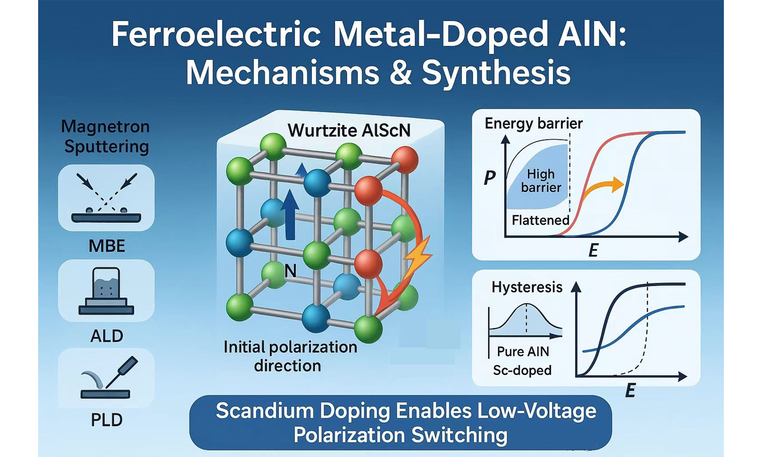
This review explores the intricate relationship between metal doping and the polarization-switching dynamics of wurtzite-phase aluminum nitride (AlN) thin films. We examine how the dopant type, concentration, and resulting crystal structure affect the ferroelectric characteristics of AlN. Particular emphasis is placed on scandium-doped AlN (AlScN), a leading candidate for next-generation ferroelectric applications. We investigate the fundamental mechanisms underlying polarization switching, emphasizing the roles of local chemical interactions, structural modifications, and domain wall dynamics. In addition, we present a comparative analysis of key synthesis techniques - including magnetron sputtering, molecular beam epitaxy, atomic layer deposition, and pulsed laser deposition - highlighting their respective advantages and limitations in fabricating high-quality ferroelectric films. By elucidating the core principles governing ferroelectricity in doped AlN, this review provides valuable insights for the design and optimization of advanced ferroelectric devices aimed at improving performance and energy efficiency.
Keywords
INTRODUCTION
Ferroelectric materials, characterized by electrically switchable spontaneous polarization, are integral to the advancement of modern technologies such as non-volatile memories, energy-efficient electronics, sensors, and neuromorphic computing systems. However, conventional perovskite ferroelectrics (e.g., PbZrxTi1-xO3) face significant challenges, including limited compatibility with complementary metal-oxide-semiconductor (CMOS) processes, environmental concerns due to lead content, and degradation at elevated temperatures. These limitations have spurred the search for alternative ferroelectrics that offer strong performance, scalable fabrication, and seamless integration with existing semiconductor platforms.
Among emerging alternatives, aluminum nitride (AlN), a III-nitride semiconductor with a wide bandgap (~6.2 eV), has garnered attention due to its exceptional properties, including high thermal conductivity, excellent chemical stability, notable piezoelectric and pyroelectric responses, and compatibility with silicon-based technologies. AlN crystallizes in the wurtzite structure, a non-centrosymmetric lattice that generates strong spontaneous polarization (~130 μC/cm2) along the [0001] c-axis. However, achieving ferroelectric switching (polarization reversal under an external electric field) typically requires electric fields exceeding its dielectric breakdown strength, rendering such switching impractical under normal conditions. Notably, ferroelectric-like switching has been observed under specific conditions, particularly in ultrathin AlN films, and theoretical studies continue to explore potential switching mechanisms. The feasibility of intrinsic ferroelectricity in pure AlN remains under investigation and appears to depend on factors such as film thickness, strain state, and defect concentration[1-4].
A major breakthrough occurred with the discovery that doping AlN with certain metals can stabilize a ferroelectric phase, significantly reducing the coercive field required for switching while maintaining - or even enhancing - the polarization magnitude. Scandium (Sc), in particular, has proven revolutionary. Alloying AlN with Sc to form Al1-xScxN lowers the coercive field (to < 5 MV/cm) and retains a high remanent polarization (> 100 μC/cm2), enabling robust switching at voltages compatible with CMOS technologies[5-8]. These properties positioned Al1-xScxN as a leading candidate for next-generation non-volatile memory (NVM) devices, energy harvesting systems, neuromorphic computing, and tunable RF components[9-12]. Beyond scandium, researchers have explored doping AlN with various other metallic elements, including Y, Mg, Ti, Cr, Zr, Nb, Hf, Ta, and W, as well as non-metallic elements such as boron (B)[13-18]. Each dopant uniquely influences the structural, electronic, and ferroelectric properties of AIN, offering a rich design space for materials engineering.
For example, boron doping can induce polarity inversion in AlN, while magnesium codoping has been shown to enhance piezoelectric coefficients. However, to date, its effect on ferroelectric behavior has not been reported[19,20]. These findings highlight the critical interplay between dopant chemistry, lattice distortion, and electronic structure in tailoring ferroelectric responses.
This review provides a comprehensive analysis of the mechanisms underpinning ferroelectric behavior in metal-doped AlN systems, with a focus on Sc-alloyed variants. We analyze the roles of dopant type, concentration, and synthesis methods in determining polarization dynamics and critically assess both experimental findings and theoretical predictions. By synthesizing recent advances, we aim to provide a roadmap for optimizing doped AlN-based ferroelectrics to meet the demands of future electronic applications.
Ferroelectric switching challenge in pure AlN: challenges and breakthroughs
Although bulk AlN possesses spontaneous polarization, it is not conventionally considered ferroelectric because of the extremely high energy barrier required for polarization reversal via atomic displacements. Theoretical calculations predict coercive fields exceeding 10 MV/cm, often surpassing AIN's dielectric breakdown strength[21]. Consequently, researchers have explored the potential ferroelectricity of undoped AlN. Yasuoka et al.[1] reported a polarization-electrical field (P-E) curve for AlN; however, the results were inconclusive, as dielectric breakdown occurred before ferroelectric switching could be verified. In contrast, Lin et al.[2] demonstrated ferroelectric behavior in ultrathin AlN films (8-10 nm) prepared via atomic layer epitaxy. They successfully induced ferroelectricity in a single-crystalline epitaxial AlN film of 8-10 nm thickness. This effect was attributed to a unique top-top configuration - two capacitors in series (Pt-AlN-GaN-AlN-Pt) - and the presence of a two-dimensional electron gas (2DEG) at the AlN/GaN interface. The 2DEG formation is driven by out-of-plane compressive and in-plane tensile strain in the [0001]-oriented AlN epilayer. However, this strain-induced mechanism becomes ineffective for thicker films (> 10nm), where the lattice mismatch at the AlN/GaN heterojunction is insufficient to sustain ferroelectricity. Hasegawa et al.[3] further demonstrated the possibility of full polarization reversal in pure, undoped AlN at room temperature. By adjusting the deposition temperature from 450 to 250 °C, they achieved complete polarization switching. At 450 °C, local polarization switching and dielectric breakdown occurred before full switching. In contrast, films deposited at 250 °C exhibited significantly higher breakdown fields, enabling full polarization reversal with a remanent polarization of 150 μC/cm2 and a coercive field of 8.3 MV/cm. The difference in behavior was attributed to variations in interface quality caused by lattice mismatch. Films deposited at higher temperatures exhibited greater mismatch and trap formation, resulting in lower leakage currents but increased susceptibility to rapid breakdown under high voltage.
Recent breakthroughs in heterostructure engineering have identified alternative strategies for enabling polarization switching in pure AlN without requiring ultrathin films or heavy doping. Skidmore et al.[4] showed that interfacial coupling between ferroelectric layers (e.g., Al1-xScxN, Al1-xBxN) and adjacent non-ferroelectric AlN layers enables full polarization reversal via proximity effects. This phenomenon is driven by elastic and electric fields generated by propagating domain walls in the ferroelectric layer, which transiently destabilize the AlN lattice and reduce the switching barrier[22,23] [Figure 1]. Proximity-induced ferroelectricity enables polarization switching in micron-thick AlN films (e.g., 500 nm AlN adjacent to
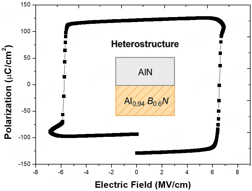
Figure 1. Polarization hysteresis loops for a 200 nm AlN|AlBN bilayer stack[24].
Therefore, achieving polarization reversal in standard AlN films is typically impractical. Drury et al.[25] investigated polarization switching in Al0.7Sc0.3N under varying temperatures and found a strong correlation between the coercive field (Ec) and thermal conditions, with Ec decreasing linearly as temperature increases. Their study confirmed stable saturation polarization across the tested temperature range (e.g., up to 400 °C). The polarization-electric field (P-E) loops exhibited a post-saturation negative slope, indicating a reduction in capacitance. This behavior is consistent with the increased current density observed in current-electric field (J-E) sweeps at higher temperatures, which demonstrated an exponential relationship between current density and electric field. Notably, Pr values for Al0.7Sc0.3N showed exceptional thermal stability, while Ec decreased linearly with increasing temperature. This trend is attributed to thermally assisted reductions in the activation energy barrier for polarization reversal. Moreover, the study acknowledged that external factors such as domain nucleation and growth - both influenced by defects and preferred crystallographic orientation - also affect Ec, particularly in conventional ferroelectric capacitors. While this trend is commonly attributed to thermally assisted domain nucleation and domain wall motion, such an explanation oversimplifies the complex interplay of mechanisms governing polarization switching. A more comprehensive analysis must account for additional factors such as strain relaxation, defect dynamics, and phase boundary interactions, which collectively modulate the switching behavior.
Strain relaxation effects
In epitaxial AlScN films grown on lattice-mismatched substrates (e.g., sapphire or silicon), thermal expansion mismatch induces residual biaxial stress. At elevated temperatures, partial strain relaxation alters the lattice parameters and internal stress state. For example, compressive strain relaxation reduces the energy barrier for polarization rotation by lowering lattice distortion energy. Substrate-induced tensile strain (commonly found in sputtered films) amplifies basal plane expansion at higher temperatures, further softening the wurtzite lattice and promoting polarization reversal through strain-polarization coupling[26-28]. This effect is particularly pronounced in films with high Sc content (x > 0.3), where structural flattening (i.e., a reduced c/a ratio) decreases steric hindrance to dipole reorientation.
Defect dynamics
Oxygen-related defects, such as substitutional oxygen impurities (ON) and associated aluminum vacancies (VAl) introduced during sputtering[29], act as charge traps and domain wall pinning centers. At elevated temperatures, increased defect mobility enables the redistribution of these impurities, reducing their inhibitory effects on domain wall motion. In parallel, nitrogen vacancies (VN), which have a higher formation energy in AlScN than in AlN, become thermally activated, forming shallow trap states that screen depolarization fields. This defect-mediated screening lowers the effective Ec by compensating for fixed polarization charges at grain boundaries and interfaces[30]. Additionally, the enhanced conductivity at high temperatures - evidenced by exponential J-E behavior - suggests that defect-assisted leakage currents partially short-circuit the depolarization field, further reducing the switching barrier.
Phase boundary interactions
In mixed-phase regions, thermal energy promotes atomic rearrangement at the interfaces between wurtzite and cubic phases. These interfaces act as nucleation sites for polarization reversal, where the coexistence of polar (wurtzite) and non-polar (cubic) phases creates localized strain gradients. These gradients stabilize intermediate switching states and effectively lower the activation energy for polarization rotation[30]. Furthermore, conductive pathways formed at phase boundaries screen long-range depolarization fields, mimicking the role of mobile charge carriers in classical ferroelectrics. This behavior is analogous to domain wall conductivity observed in oxide ferroelectrics, where metallic-like conduction along domain walls reduces the switching energy[31].
These mechanisms are not mutually exclusive but rather operate synergistically. For example, strain relaxation enhances defect mobility by reducing lattice rigidity, while phase boundary interactions facilitate defect segregation at interfacial regions. This multifaceted interaction helps explain why the reduction in Ec becomes more pronounced and nonlinear at higher Sc concentrations (x > 0.3), where structural softening and defect density simultaneously peak.
This understanding opens new avenues for optimizing deposition parameters to achieve higher polarization values and lower coercive fields in undoped AlN. Two main strategies can be considered to address the challenge of reducing Ec. The first involves engineering well-established wurtzite materials such as AlN and ZnO through alloying and strain application[32,33]. The second focuses on the investigation and synthesis of novel wurtzite-type materials that inherently possess lower coercive fields[34,35]. A key objective is to elucidate the underlying polarization switching mechanisms and clarify the structure-property relationships that influence Ec. Ultimately, it is essential to identify structural deviations from the conventional wurtzite configuration that facilitate the transition from positive to negative polarization.
Doping strategies to induce ferroelectricity
Polarization switching refers to the ability of a ferroelectric material to reverse the direction of its spontaneous electric polarization under an applied electric field. This property is critical for numerous electronic applications, including non-volatile memories and sensors[36]. However, the polarization-switching behavior of wurtzite AlN thin films remains poorly defined. Incorporating specific metal cations at the Al sites within the AlN lattice has been shown to effectively reduce the energy barrier for polarization switching.
Boron doping exemplifies how local chemical disorder can stabilize metastable states that are crucial for switching. Studies on Al0.93B0.07N thin films have demonstrated remnant polarization values exceeding
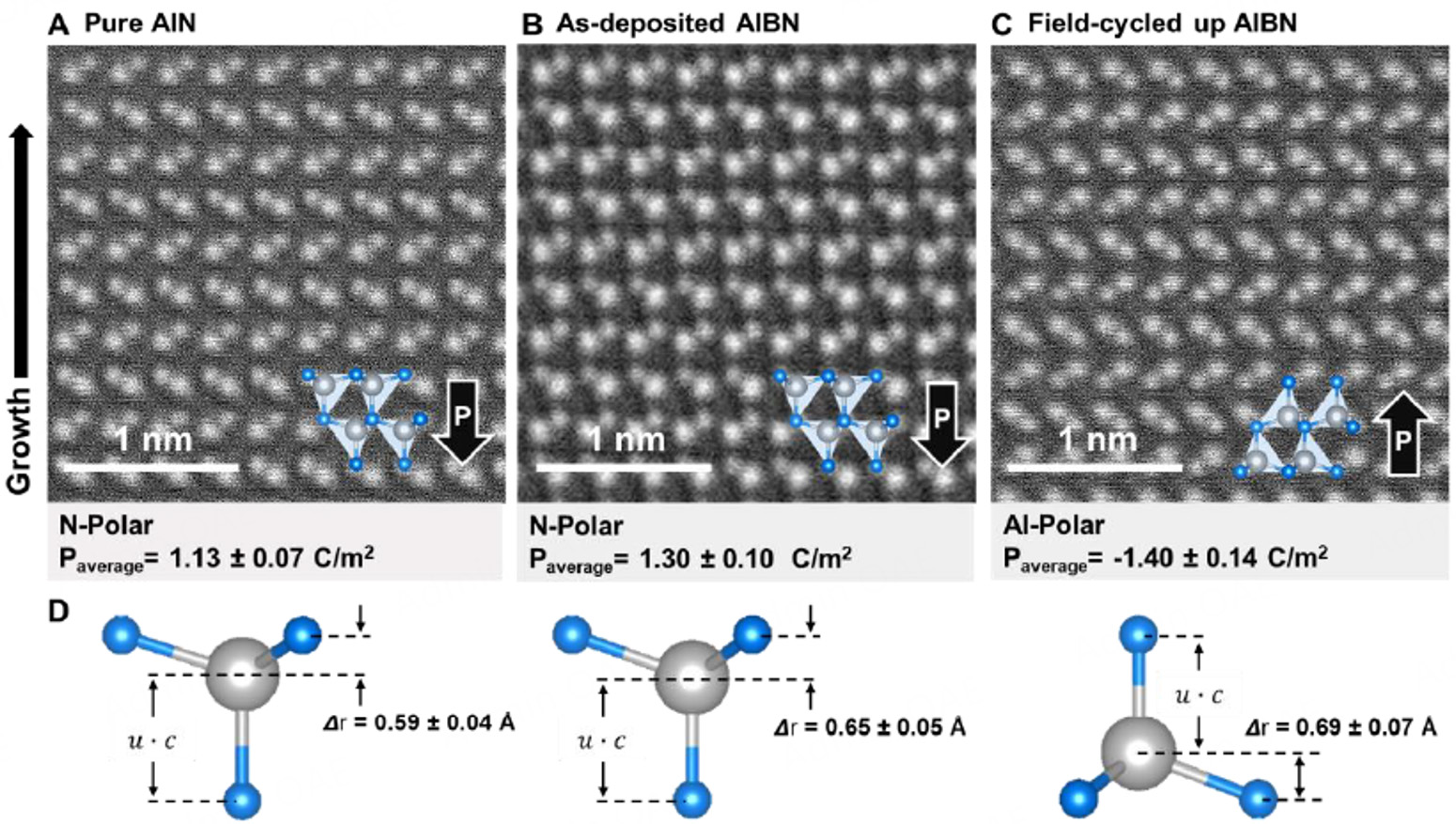
Figure 2. (A-C) dDPC images for pure AlN, as-deposited Al0.94B0.06N, and field-cycled Al0.94B0.06N. (D) Schematic of structural modifications following boron incorporation and field cycling[23].
In addition to chemical doping strategies, structural optimization through interlayer (IL) engineering in AlScN ferroelectric diodes has emerged as a promising approach. By incorporating a 0-5 nm AlOx IL into a metal/ferroelectric/insulator/metal (MFIM) architecture, ON/OFF ratios exceeding 3,000 and rectification ratios above 5,000 were achieved in 10 nm Al0.72Sc0.28N devices[5]. The IL suppresses direct tunneling currents in the high-resistance state while enhancing polarization-driven electrostatic modulation, which is critical for high-density crossbar arrays. This structural optimization mirrors the advantages of defect engineering observed in B-doped systems, effectively addressing leakage issues in scaled geometries. The approach modifies both the crystal structure and electronic interactions, enabling polarization reversal under more accessible electric fields.
However, doping-free approaches that leverage interfacial proximity effects are now emerging as complementary strategies. Traditional methods to induce ferroelectricity in wurtzites, such as Sc or B substitution in AlN[5], introduce scattering centers that degrade thermal and electronic properties. Proximity-induced ferroelectricity circumvents these trade-offs, preserving the pristine characteristics of unmodified AlN and ZnO, which are vital for high-frequency optoelectronics and power devices. This concept builds upon the polar discontinuity model proposed by Stutzmann et al.[22] for GaN/AlN junctions, extending it to demonstrate dynamic reconfigurability rather than relying solely on static polarization engineering. For example, hybrid nitride-oxide stacks (e.g., AlBN/ZnO) exhibit a reduced coercive field
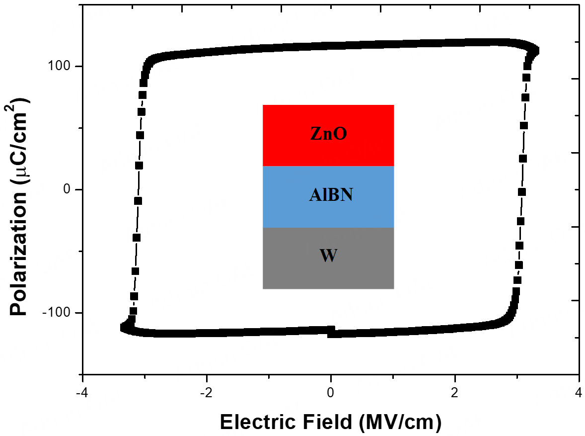
Figure 3. Polarization hysteresis loops for a heterojunction capacitor comprising 250 nm ZnO/200 nm Al0.94B0.06N/100 nm W[24].
The type and concentration of a dopant can influence the polarity of a film, the magnitude of its polarization, and its switching behavior. For example, doping wurtzite AlN with Si can invert the film’s polarity from Al-polar to N-polar. Ge doping can also reverse the polarity, although the resulting switching behavior differs. In contrast, Mg doping increases the magnitude of polarization without altering the film’s polarity. Various switching mechanisms have been proposed for wurtzite AlN thin films, including domain wall motion, charge injection, and defect-assisted switching. Different dopants can affect these mechanisms in distinct ways. For example, Si doping promotes the formation of domain walls, thereby enhancing switching behavior. Ge doping, on the other hand, facilitates charge injection, which also contributes to improved switching performance. Aluminum scandium nitride (Al1-xScxN) is a ternary compound with a wurtzite crystal structure similar to that of AlN. However, as the ionic radius of Sc is larger than that of Al, Sc incorporation causes lattice distortion in the Al1-xScxN wurtzite structure. This distortion significantly impacts the compound’s properties, particularly its optical and ferroelectric characteristics.
Metal dopants can be classified into two performance tiers based on their ability to optimize key ferroelectric parameters: Pr and Ec. Sc-doped AlN, the focal point of this analysis, falls into the high-performance tier due to its exceptional ability to achieve Pr ≥ 100 µC/cm2 and reduce Ec to ≤ 5 MV/cm at moderate doping levels (x~0.3). This performance surpasses that of alternative rare earth dopants, such as yttrium (Y), lanthanum (La), and certain transition metals (e.g., Mg, Zn). For instance, Al1-xYxN can reach
In comparison, dopants such as Mg and Zn are categorized in the standard performance tier. Although well-established and widely used, these dopants generally fail to meet the performance requirements for applications demanding high efficiency and low power consumption. The selection of a dopant involves a complex trade-off among several factors, including cost, process compatibility, and device performance. While Sc-doped AlN offers superior efficiency, its higher cost and potential fabrication challenges may limit widespread adoption. Nevertheless, recent research has demonstrated methods to reduce the switching voltage in Al1-xScxN films by modifying the material structure or experimental setup. Strategies include adjusting the testing temperature[42], increasing the Sc content[1], enhancing crystallinity[43,44], and employing alternative substrates[6] - all of which have shown effectiveness in lowering the required switching voltage while maintaining high polarization values. As these technologies mature, the cost of Al1-xScxN is expected to decline, making it more viable for commercial applications.
Al1-xScxN exhibits superior properties compared to traditional aluminum nitride (AlN), including an enhanced piezoelectric coefficient and improved electromechanical coupling, owing to the substitution of Al with Sc[45]. This material overcomes the ferroelectric limitations of AlN thin films while maintaining excellent high-temperature stability, CMOS compatibility, and mechanical robustness[46]. Like AlN, Al1-xScxN has a wurtzite crystal structure, with atoms arranged in a hexagonal pattern[47]. Wurtzite-structured doped III-nitrides offer significant advantages, such as scalability, compatibility with existing manufacturing procedures, and strong ferroelectric performance. These materials are well-suited for large-scale applications, such as displays and memory devices, and can be fabricated using established III-V semiconductor processing techniques[48-51]. Moreover, their strong ferroelectric properties make them ideal candidates for high-performance electronic applications. However, the exact origin of ferroelectric behavior in Al1-xScxN wurtzite structures remains incompletely understood. It is believed to be influenced by several factors, including the local chemical environment, extended structural characteristics, and the presence of intrinsic defects.
In addition to the ferroelectric response in doped III-N wurtzite structures being of interest to researchers for three main reasons, several other factors contribute to their growing appeal. One notable advantage is their tunable properties[52], which can be modulated by adjusting the type and concentration of dopants as well as the growth conditions. This tunability makes them highly versatile for tailoring specific ferroelectric characteristics. Furthermore, doped III-N wurtzite materials can be integrated with other III-V semiconductors and silicon[13], making them promising candidates for heterogeneous integration - an essential technology for future electronic devices. Among these materials, Al1-xScxN, which possesses a distinct wurtzite structure, exhibits limitations for certain applications. In particular, its piezoelectric coefficient is relatively low compared to alternative materials, which restricts its applicability. Nevertheless, the thin-film piezoelectric device market is rapidly expanding. According to the Business Research Company, this market was valued at approximately $3,860.5 million and is projected to reach
Pi = dijkσjk + εijEj, where the piezoelectric coefficient dijk depends on the material’s Born effective charge (Z*), elastic compliance, and polarization susceptibility. Sc3+ substitution elongates the cation-anion bond length (e.g., Sc-N vs. Al-N), increasing bond polarizability and enhancing Z*, which reflects the dynamic contribution to polarization per unit atomic displacement. Additionally, lattice distortion alters the electronic structure, further impacting Z*. The resulting dipole moment (μ = Z*·δr), where δr is the relative ion displacement under strain, increases due to both a higher Z* and a larger δr, the latter resulting from softer bonds in the strained lattice. Together, these factors significantly enhance the intrinsic piezoelectric response under applied stress. Moreover, the enhancement of piezoelectricity in ABN compounds also depends on the type of B-site element. The highest piezoelectric constants are observed in systems where Al is the B-site element, followed by Ga and In. This trend is attributed to the stronger covalent bonding in Al-N compared to the more ionic nature of Ga-N or In-N. Strong covalent bonds in Al-N enable structural integrity under strain while allowing reversible ionic displacement. In contrast, Ga-N and In-N bonds reduce lattice rigidity and increase inharmonic phonon scattering, thereby dissipating piezoelectric energy. However, achieving high concentrations of A-site dopants (e.g., in Al1-xScxN with x > 0.5) is constrained by phase instability. At elevated Sc content, the metastable wurtzite phase tends to transition to a non-piezoelectric cubic phase. It has been predicted that a higher piezoelectric effect can be achieved at higher Sc ratios if the wurtzite phase can be stabilized against this transformation. This stabilization may be facilitated by introducing a third dopant element, which could reduce coherency strain and suppress cation migration, thereby extending the compositional range conducive to high piezoelectricity. This highlights the need to balance ionic size mismatch, bond strength, and phase stability to optimize electromechanical coupling in nitride-based piezoelectrics. In this context, the use of a seed layer offers a viable strategy. According to Höglund et al.[54], (cubic)-Al1-xScxN solid solutions deposed using ScN seed layers can be synthesized with AlN molar fractions up to ~60%. The transition from a mixed-phase (wurtzite + cubic) to a purely cubic phase occurs at around x ≈ 0.5, depending on the specific seed layer and growth conditions.
Furthermore, the large-scale fabrication of doped AlN remains challenging and must be addressed to enable commercial viability. These challenges have limited the development of AlN - particularly doped wurtzite films such as Al1-xScxN - for use in piezoelectric, ferroelectric, and FeRAM applications. Notably, although sputter deposition is commonly employed for AlN films in these applications due to its compatibility with CMOS processes, residual oxygen or water vapor in vacuum chambers can introduce oxygen-related defects (e.g., Al vacancies and O substitution), which disrupt crystallinity and increase leakage currents, ultimately compromising device reliability[29]. Temperature-dependent I-V analysis confirms that Poole-Frenkel emission (J ∝ e-1/T) dominates the low-resistance state, while thermionic emission (J ∝ T2e-1/T) governs the high-resistance state at low biases[5]. These phenomena necessitate ultra-high vacuum (UHV) conditions
Al-Sc-N system: the leading candidate
Incorporating specific metal cations into Al sites within the AlN lattice has proven effective in lowering the energy barrier for polarization switching, thereby inducing or stabilizing ferroelectricity. This strategy modifies the crystal structure and electronic interactions, enabling polarization reversal under accessible electric fields. Among the dopants explored, Sc has garnered the most attention due to its dual role in disrupting local chemical bonding and inducing global structural distortions. Other dopants have also been investigated, leading to a broad family of ferroelectric wurtzite nitrides.
AlN is a III-V compound semiconductor, composed of aluminum from group III and nitrogen from group V of the periodic table. This composition imparts AlN with a wide range of functional properties, especially in optoelectronic applications[56]. AlN typically crystallizes in the wurtzite phase, where each Al atom is tetrahedrally coordinated to four nitrogen atoms through covalent bonds [Figure 4].
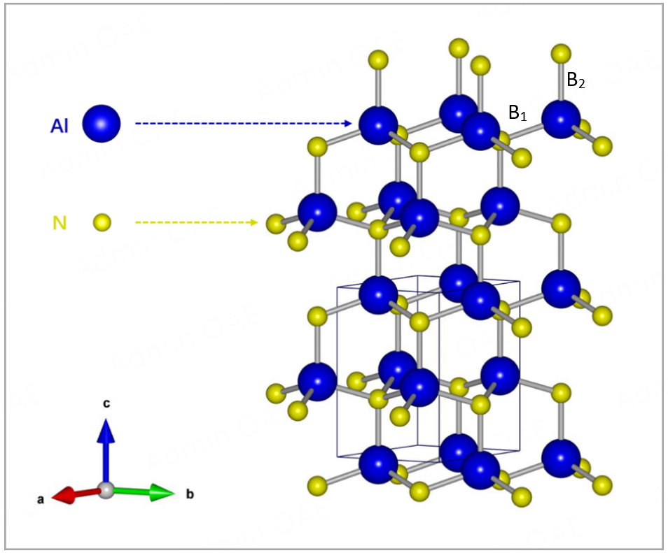
Figure 4. Crystalline structure of AlN in the wurtzite phase.
In the AlN wurtzite structure, the bond along the c-axis (0001 direction), referred to as B2, is slightly longer (1.90 Å) than the three equivalent B1 bonds (each 1.89 Å). This subtle asymmetry highlights the non-centrosymmetric nature of the AlN unit cell, a key factor underlying its piezoelectric behavior. Even in the absence of external electrical or mechanical stimuli, AlN films exhibit a spontaneous polarization in their charge distribution. The wurtzite phase represents the thermodynamically stable configuration of AlN. Due to the polarity along the [0001] and [000-1] directions, surface terminations can be either Al-polar or N-polar. In Al-polar surfaces, aluminum atoms are positioned at the top of the diatomic layer, while in N-polar surfaces, nitrogen atoms occupy the apex. For Al-polar configurations, the c-axis aligns with the internal electric field extending from the substrate to the surface, resulting in a polarization direction opposite to the field. This leads to positive polarization-induced fixed charges at the substrate interface and negative charges at the surface. In contrast, this relationship is reversed for N-polar surfaces.
AlN exhibits a spontaneous polarization of approximately 0.08 C/m2[57], confirming its pyroelectric nature. Its specialized crystalline structure offers excellent thermal and chemical stability, high thermal conductivity (~320 W/m•K), and a melting point of around 2,800 K, which exceeds that of zinc-blende AlN
Structure evolution and phase transition in Al1-xScxN
The substitution of aluminum atoms in AlN with scandium was first intensively studied by a Japanese team. They demonstrated that Al1-xScxN films (0.1-1.1 μm thickness, x = 0.43) exhibit a significantly enhanced piezoelectric coefficient, with d33 increasing from 5.5 pC/N for pure AlN to 27.6 pC/N for Al1-xScxN - a fivefold improvement[60]. Structural analysis indicates that Sc has limited solubility in AlN, resulting in three distinct phases depending on Sc concentration:
• Wurtzite phase for x < x1
• Mixed phase (wurtzite + cubic) for x1 < x < x2
• Cubic phase for x > x2
The bandgap evolution in AlScN as a function of Sc content can indicate possible structural transitions. Deng et al.[61] demonstrated that the optical absorption spectra of Al1-xScxN films, grown on sapphire (0001) substrates via reactive magnetron co-sputtering, exhibited a nearly linear decrease in bandgap energy for
Dual mechanisms of ferroelectric enhancement
Doping AlN with Sc (or alloying it with ScN) significantly enhances its ferroelectric response through two distinct mechanisms:
- Local chemical bonding effects: The larger ionic radius of Sc3+ (0.88 vs. 0.54 Å for Al3+) disrupts the covalent sp3 bonding network of AlN, causing bond frustration. Sc prefers octahedral coordination (via sd3 hybridization) over tetrahedral, introducing localized strain fields that lower the Peierls-Nabarro barrier for domain wall motion.
- Global structural flattening: Increasing Sc content reduces the c/a ratio of the wurtzite lattice, promoting a flatter structure and enabling polarization rotation via a proposed metastable hexagonal (H) phase.
Höglund et al.[27] investigated Al1-xScxN films through structural characterization and first-principles calculations for x values from 0 to 0.78. Their results indicated the formation of a disordered single-crystal solid solution in the wurtzite phase (w-Al1-xScxN), with a solubility limit of ScN in AlN at 22%. For x < 0.22, the c-parameter remains nearly constant, while the a-lattice parameter increases linearly due to the larger Sc ionic radius. Specifically, the a-parameter increases from 3.11 to 3.21 Å as x increases from 0 to 0.22, while the c-parameter shows minimal change. As Sc content increases between 23% and 50%, nanocrystalline mixtures of ScN and AlN form, and at higher concentrations, a cubic Al1-xScxN phase becomes dominant. Notably, in the composition range 0.4 < x < 0.55, the wurtzite, cubic, and hexagonal phases can coexist. Increasing Sc content also leads to a decline in crystal quality due to higher defect intensities and local deformations. Nonetheless, the films maintain a disordered single-crystal solid solution structure, with randomly distributed Al and Sc atoms - typical of ternary alloys - and this randomness is believed to enhance the piezoelectric performance of Al1-xScxN.
The effect of Sc concentration on the piezoelectric properties of Al1-xScxN provides insights into the origins of ferroelectric behavior. Using first-principles calculations, Tholander et al.[65] and Tasnádi et al.[45] found that the enhanced piezoelectric response is intrinsically linked to local coordination competition in different environments, driven by the metastable layered hexagonal phase of ScN. Polarization changes primarily result from lattice distortions surrounding Sc sites, underscoring the importance of local atomic environments. At x = 0.5, the observed peak in piezoelectric constants is attributed to strong competition between Al and Sc atoms for bonding with nitrogen, particularly between the h-ScN and α-AlN phases. Sc’s preference for hexahedral coordination introduces structural frustration, amplifying the material’s response to strain. Thus, the hexagonal structure of ScN plays a crucial role in enhancing piezoelectricity, confirming that intrinsic alloy effects are the primary drivers of the observed improvements in Al1-xScxN.
Umeda et al.[66] performed first-principles calculations and experiments to study the structural and piezoelectric properties of Al1-xScxN alloys. They observed that increasing the Sc concentration led to a reduction in the c/a lattice ratio, which corresponds to an increase in the hexagonal structure parameter. This parameter reflects the ratio between the bond length along the c-axis and the c-lattice constant, effectively characterizing the interplanar distance between metal and nitrogen atoms. Experimentally, for Sc concentrations up to 0.5, they reported a linear increase in the c-lattice constant up to a Sc ratio of 0.2, followed by a rapid decrease up to 0.4. This structural flattening (i.e., reduction in the c/a ratio) was found to correlate with enhanced piezorelectric coefficients d33 and d31, which was attributed to increased mobility of Al atoms along the c-axis[66]. Electron probe microanalysis revealed that scandium substitution reduces the spatial occupancy of Al atoms, causing lattice distortion during the phase transition process[67]. This transition from a hexagonal to a cubic structure induces a 14-fold increase in the piezoelectric coefficient. However, when the scandium concentration exceeds x = 0.3, the cubic structure becomes energetically more favorable, leading to a sharp decline in piezoelectric response. They suggest that the maximum piezoelectric response occurs in a mixture of polar wurtzite AlN and non-polar cubic ScN (if the wurtzite structure is maintained). This is plausible because the polar wurtzite structure exhibits piezoelectricity, while the cubic structure does not. The authors believe that combining these two structures could yield material benefits from both the piezoelectric properties of wurtzite and the structural stability of the cubic phase. However, this remains a theoretical concept, as no experimental studies have yet succeeded in creating such a material. Further research is required to determine whether this can be achieved.
The phase transition from wurtzite to cubic rocksalt also reveals discrepancies between Density Functional Theory (DFT) predictions and experimental observations. DFT calculations, such as those by Talley et al.[68] (x = 0.64) and Furuta et al.[69] (x = 0.67), predict a sharp compositional threshold for the phase transition under equilibrium conditions. In contrast, experiments consistently reveal mixed-phase coexistence (wurtzite and cubic) during the transition, influenced by scandium concentration, deposition parameters, substrate properties, and kinetic effects. These discrepancies arise from inherent differences between idealized theoretical models (which assume equilibrium and defect-free systems) and real-world synthesis methods such as magnetron sputtering, where rapid growth rates and limited adatom mobility prevent complete atomic rearrangement and stabilize metastable mixed phases.
Additionally, defects (e.g., vacancies, dislocations) and substrate-induced strain fields can act as nucleation sites for cubic domains or disrupt long-range ordering, thereby promoting phase coexistence. Experimental systems also face thermodynamic limitations: while DFT predicts phase separation into AlN and ScN due to the positive mixing enthalpy, kinetic freezing during deposition traps Sc in a metastable solid solution. Substrate interactions add further complexity. For example, epitaxial strain from sapphire (0001) can stabilize cubic phases at lower x or alter lattice parameters, resulting in deviations from bulk predictions. Moreover, configurational entropy at deposition temperatures (absent from 0 K DFT models) contributes to the stabilization of disordered alloys. Post-deposition annealing studies highlight the role of kinetics: prolonged thermal treatment reduces mixed-phase regions, bringing experimental outcomes closer to DFT predictions. Thus, the discrepancies between theory and experiment reflect a complex interplay of thermodynamic driving forces, kinetic limitations, defect dynamics, and strain engineering, factors that are critical for optimizing the functional properties of AlScN in next-generation electronic devices. DFT’s reliance on periodic boundary conditions and simplified supercell approximations limits its ability to capture nanoscale heterogeneity and localized strain gradients observed in experimentally observed mixed-phase systems. Höglund et al. conducted ab initio calculations to assess the mixing enthalpy of wurtzite AlN, rocksalt ScN, and layered hexagonal ScN[27]. Their results indicate that AlScN transitions from a hexagonal to a cubic rocksalt structure at x ≈ 0.56. However, the positive mixing enthalpy suggests thermodynamic instability, favoring phase separation into pure AlN and ScN. Despite this, kinetic limitations (e.g., low diffusion rates during growth) and defect-stabilization mechanisms allow the metastable phase to persist. For example, Sc-rich clusters or interfacial strain at grain boundaries can locally stabilize cubic regions even below the theoretical transition threshold. These factors, combined with deposition-specific parameters (e.g., nitrogen partial pressure, substrate bias), create a complex energy landscape where phase evolution is pathway-dependent rather than purely composition-driven. Understanding these dynamics is essential for device fabrication, as the coexistence of wurtzite and cubic phases in the 0.4 < x < 0.55 range offers unique electromechanical properties - requiring precise process control to optimize phase purity and performance.
The disparity between DFT and experimental observations in Al1-xScxN phase transitions stems from the combined effects of kinetic limitations, defect dynamics, strain, and entropy - factors often omitted in theoretical models. A holistic understanding requires the integration of ab initio insights with mesoscale phenomena (e.g., defect distributions, strain relaxation) and process-dependent kinetics. Advances in computational methods, such as machine-learning force fields and phase-field modeling, could bridge this gap by simulating larger-scale, defect-laden systems under non-equilibrium conditions. Experimentally, in situ characterization during growth (e.g., XRD, TEM), paired with controlled annealing studies, will further elucidate the kinetic pathways governing phase evolution, enabling the precise tuning of AlScN’s functional properties.
Ferroelectric behavior and polarization switching
The first demonstration of ferroelectricity in the III-V semiconductor AlN doped with Sc was reported by Fichtner et al.[46], providing evidence that the observed P-E hysteresis loops result from true ferroelectric behavior. Specifically, the wurtzite crystal structure is conserved during the application of a switching field, and polarization switching occurs at the unit-cell level in Al1-xScxN. This switching process involves the cooperative displacement of Al3+/Sc3+ cations relative to the N3- sublattice within a softened double-well potential energy landscape. While undoped AlN requires a coercive field higher than its breakdown strength to reverse polarization, increasing the Sc content significantly lowers this barrier. For instance, the coercive field decreases from 5 MV/cm in Al0.73Sc0.27N (x = 0.27) to below 2 MV/cm in Al0.57Sc0.43N (x = 0.43), while maintaining a remanent polarization exceeding 100 μC/cm2[46]. Lu et al.[70] further investigated the field-dependent switching dynamics in 20-nm-thick Al0.72Sc0.28N capacitors, revealing a transition from nucleation-limited switching (NLS) at low electric fields (< 1.5 Ec) to Kolmogorov-Avrami-Ishibashi (KAI)-like kinetics at higher fields (> 1.5 Ec). Similar frequency-dependent polarization dynamics are observed in B-doped AlN (Al0.93B0.07N), where the time under an applied field (cycles/frequency) governs the wake-up behavior[37]. This phenomenon is driven by an unusually high activation field (α ~ 126 MV cm-1), two orders of magnitude larger than that of perovskite ferroelectrics such as Pb(Zr,Ti)O3. As a result, switching times can be reduced by 5-6 orders of magnitude with only moderate field increases (1.2-2 Ec)[37,71]. These ultrafast switching kinetics, attributed to Sc-induced lattice softening and defect-mediated nucleation, underscore the potential of AlScN for high-speed, non-volatile memory applications.
Studies on epitaxial AlScN/GaN heterostructures further highlight the interplay between interfacial stability and polarization dynamics. Wang et al. demonstrated that Al0.82Sc0.18N undergoes rapid surface oxidation upon air exposure[72], forming a disordered oxide layer rich in Sc-O and Al-O bonds.
This oxidation introduces a secondary valence band edge at ~6 eV in XPS measurements, complicating the accurate determination of intrinsic band alignment. However, when samples are maintained under vacuum, the intrinsic type-II band alignment of Al0.82Sc0.18N/GaN is preserved, revealing a valence band offset of
The reduction in switching barriers is theorized to involve metastable hexagonal phase intermediates that emerge during polarization rotation. Although direct experimental evidence for this phase in pure AlN remains lacking - due to its high formation energy - recent atomic-scale studies on Al0.94B0.06N thin films using differential phase contrast scanning transmission electron microscopy (DPC-STEM) have confirmed the presence of such intermediate states. These studies reveal a transient nonpolar geometry during the switching process [Figure 5][23].
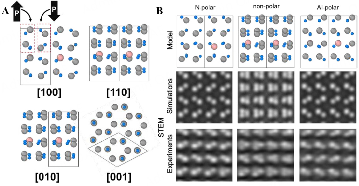
Figure 5. Nudged-elastic-band simulation of polarization reversal pathways. (A) Structural model of the nonpolar transient state calculated for Al15/16B1/16N, viewed along different projections. (B) Atomic models, STEM image simulations, and experimental images of the N-polar, nonpolar and Al-polar states[23].
In Al-B-N systems, polarization reversal proceeds through a sequential antipolar phase that reduces the switching barrier by 60% compared to pure AlN. First-principles simulations corroborate this mechanism, showing that alloying elements such as B or Sc introduce bond frustration and stabilize transient states, thereby enabling domain wall nucleation and propagation under lower electric fields[38].
Further direct evidence of this mechanism comes from piezoresponse force microscopy (PFM) imaging by Lu et al.[70], who observed domain nucleation rates as high as 1014 m-2 and domain wall velocities ranging from 10-4 m/s (4.5 MV/cm) to 1 m/s (6.5 MV/cm). These observations align with DFT predictions of transient nonpolar states during switching[73]. Partial polarization reversal generates polydomain states with inclined 180° domain walls, which Lu et al.[70] demonstrated to enhance steady-state conductance by up to two orders of magnitude compared to monodomain configurations [Figure 6].
Figure 6. I-V measurements of steady-state conductance in 20-nm-thick Al0.72Sc0.28N capacitors during various switching stages. (A) PFM images of the domain structures at each switching stage with a fixed poling voltage of 13 V. (B) Corresponding I-V characteristics. (C and D) Estimated polarization switching fractions (percentage of domains in the upward state) (C), and corresponding leakage currents at 4 V (D) for each switching stage[70].
This phenomenon, attributed to conductive domain walls acting as nanoscale current pathways, mirrors STEM observations in Al0.74Sc0.26N[6] and aligns with theoretical models of conductivity induced by polarization discontinuities. Atomic-scale evidence of polarization reversal mechanisms in wurtzites was provided by Schönweger et al.[6], who used aberration-correction STEM to visualize inclined 180° inversion domain boundaries (IDBs) within single-nanometer grains of Al0.74Sc0.26N [Figure 7].
Figure 7. ABF-STEM micrograph showing the Pt/Al0.74Sc0.26N/Pt/GaN capacitor stack in cross-section. (A) The inset shows superimposed EDS maps of Pt, Al, and Ga. (B) Atomic structure sketches of M- and N-polar states. (C) Inverted ABF-STEM micrograph sketches of an inclined inversion domain boundary separating M-polar (upper right) and N-polar (lower left) regions, with overlaid (Al,Sc)-N dumbbell schematics indicating polarization direction. (D) Intensity profiles of polarization direction within individual (Al,Sc)-N dumbbells, with arrows indicating profile direction and color-coded polarity: M-polarity = pink, N-polarity = blue[6].
These IDBs exhibit horizontal polarization discontinuities, challenging classical vertical domain wall models. The presence of sub-grain domains supports analog-like switching via domain wall motion, a feature essential for neuromorphic computing. Notably, partial polarization reversal within grains enables multi-state operation - a phenomenon previously theorized but not yet observed in wurtzite systems.
However, ferroelectricity is stable only within a limited Sc concentration range (x < ~0.5). Beyond this threshold, excessive Sc incorporation destabilizes the wurtzite structure, leading to phase segregation or a transition to non-ferroelectric cubic phases, thereby suppressing switchable polarization. The coercive field can also be modulated by increasing tensile strain, for instance by adjusting the Ar partial pressure in the sputter gas. Tensile strain amplifies basal plane expansion, reducing switching barriers through strain-polarization coupling. These findings establish Al1-xScxN as a tunable ferroelectric system - provided the Sc content remains below its phase-stability limit (~x = 0.5) - paving the way for novel III-N-based ferroelectric devices.
One key challenge for advancing and enabling mass production of efficient devices is understanding the origin of ferroelectricity in the wurtzite structure. Two main perspectives are considered: (1) local chemical effects involving structural instabilities; and (2) extended structural effects such as lattice flattening. However, the origin remains incompletely understood. The main hypotheses include:
• Local chemical effects: Ferroelectric behavior arises from atomic-level instabilities caused by defects (e.g., vacancies or interstitials) or substitutional disorder. Sc doping introduces bond frustration between tetrahedral Al3+ and octahedral Sc3+ coordination, disrupting the sp3 covalent network and lowering polarization stability.
• Structural modification: Ferroelectricity may also be linked to the arrangement of atomic layers, particularly under high defect concentrations or external stress. Global lattice flattening (reduced c/a ratio) enables polarization rotation via a metastable hexagonal (H) phase. However, DFT calculations show that this contributes < 15% to the overall switching energy reduction, with local bond ionicity playing a more dominant role.
A synergistic mechanism is likely: local Sc-N ionic bonding reduces the intrinsic energy barrier for polarization rotation, while structural flattening (reduced c/a ratio) stabilizes intermediate states, enhancing ferroelectric switching (e.g., through the H-phase). Isolating local and global structural effects remains difficult, as traditional tools like X-ray diffraction (XRD) and PFM provide only averaged material properties. Advanced 4D-STEM now enables mapping of polarization vectors at atomic resolution, revealing domain wall pinning at Sc-rich clusters. Another challenge lies in the strong sensitivity of wurtzite ferroelectricity to composition and growth conditions, complicating reproducibility and hindering comprehensive understanding. Despite this, significant progress has been made through advanced tools such as scanning transmission electron microscopy (STEM) and atom probe tomography, which enable detailed characterization of local structures. For instance, 4D-STEM can resolve transient H-phase domains during switching by tracking lattice parameter evolution at nanosecond timescales. A deeper understanding of these mechanisms will facilitate the design of new materials with optimized ferroelectric properties, supporting the development of next-generation devices.
Impact of scandium concentration on lattice parameters
The evolution of lattice parameters in Al1-xScxN thin films reflects a complex interplay between Sc-induced strain and phase stability. Satoh et al.[74] studied structural deformation and phase transitions in Al1-xScxN as Sc content varied from 0 % (AlN) to 100% (ScN). The wurtzite phase remains stable up to x = 0.3. Between
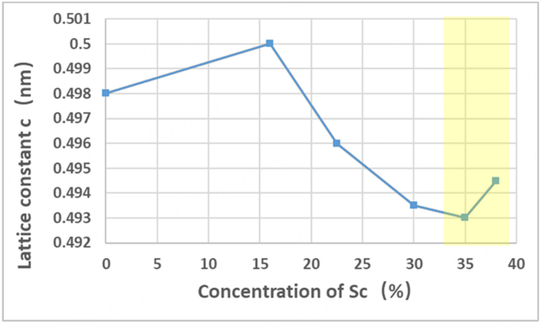
Figure 8. Dependence of the c-axis lattice constant on Sc concentration in Al1-xScxN. The two-phase coexistence region is highlighted in yellow. Adapted from Ref.[74].
Lu et al. further linked these structural changes to switching dynamics[70], showing that reduced c/a ratios at x = 0.28 decrease steric hindrance for polarization rotation, enabling domain wall velocities > 1 m/s under fields > 6 MV/cm. This interplay between lattice flattening and Sc-N bonding underpins Sc’s dual role in enhancing both piezoelectric and ferroelectric properties.
This analysis highlights the substrate's significant role in the evolution of lattice parameters. Both studies, anchored in experimental data, reveal similar trends; however, Satoh et al. specifically observed a notable decrease in the c-axis lattice parameter with increasing Sc content when the films were deposited on sapphire substrates[74]. This effect is attributed to sapphire-induced biaxial tensile strain, which promotes basal plane expansion and amplifies the lattice-distorting influence of Sc. These findings underscore the importance of substrate effects on lattice dynamics. The observed changes likely result from localized interactions between Sc and Al atoms in the lattice. In the mixed-phase region, the Sc concentration is higher in the cubic phase than in the wurtzite phase, leading to a relief of c-axis distortion in residual wurtzite domains once the Sc ratio exceeds 0.35. This phase segregation occurs because of Sc3+’s preference for octahedral coordination, driving its incorporation into the cubic phase. At lower Sc content (x = 0 to 0.16), substitution into Al sites introduces lattice strain and distortion, causing expansion along the <110> direction and increasing both a and c lattice constants. Initially, this trend follows Vegard’s law, but above
Substrate and strain effects
Substrate-induced strain, interfacial interactions, and growth templating critically influence lattice parameters and phase stability in thin films. Substrate engineering is key to stabilizing metastable wurtzite phases, minimizing defects, and optimizing ferroelectric performance. For instance, Zheng et al.[7] employed c-axis sapphire substrates with epitaxial <111>Al bottom electrodes to grow highly oriented Al0.72Sc0.28N films. The high thermal boundary conductance of Al/sapphire suppressed hillock formation during 350 °C deposition, yielding smooth, defect-free Al layers[77]. Cross-sectional TEM confirmed sharp Al/AlScN interfaces, crucial for minimizing leakage currents in sub-10 nm films. In contrast, Si-based substrates suffer from lattice mismatch and interfacial oxide formation, degrading ferroelectric performance[70]. Strain effects differ by substrate: silicon induces compressive strain that stabilizes the wurtzite phase up to x = 0.35, while sapphire substrates impose biaxial tensile strain, amplifying basal plane expansion[74,75]. Zheng et al. demonstrated that Al template-induced in-plane compressive strain on sapphire yields out-of-plane tensile strain in AlScN, increasing the c-axis lattice parameter from 5.01 Å (27 nm film) to 5.07 Å (5.4 nm film)[7]. Strain engineering also mitigates premature capacitor breakdown, a common issue in polycrystalline films on Pt or Si.
Seed layers and buffer materials further expand the scope of substrate engineering strategies. Saha et al.[28] reported a phase transition from the wurtzite to a mixed phase at Sc concentration of 0.28, and demonstrated the stabilization of cubic AlScN (0.62 ≤ x ≤ 0.82) using a TiN buffer layer on MgO. The TiN lattice (≈ 4.24 Å) acts as a template for cubic AlScN, reducing interfacial energy. This stabilization is critical, as it enables the growth of Al1-xScxN films with a wurtzite structure even at high scandium concentrations. Momida et al.[40] found that their DFT results aligned well with experimental c-axis trends up to Sc = 0.2, but diverged at higher concentrations (x > 0.5), where DFT underestimates bond frustration in the solid solution. Seed layers also critically influence phase integrity. Höglund et al.[54] showed that ScN seed layers promote cubic symmetry up to 60% Sc, while AlN seed layers preserve the wurtzite phase up to Sc = 0.48. These interactions may influence the piezoelectric response more significantly than lattice changes alone. In addition to phase stabilization, seed layers enable control over film polarity. Growth mechanisms further affect polarity: Milyutin et al.[78] achieved Al-polarity in sputter-deposited AlN using MOCVD seed layers, which favor layer-by-layer growth (75% Al termination) over stochastic sputtering. Similarly, Zheng et al.[7] demonstrated that epitaxial Al electrodes act as effective growth templates, minimizing defects and interfacial charge traps - crucial for reliable performance in sub-10 nm ferroelectric devices.
A landmark study by Yasuoka et al.[79] established a connection between substrate-induced strain and crystal anisotropy. By depositing Al0.8Sc0.2N films on fused silica, Si, Al2O3, and MgO substrates with varying thermal expansion coefficients αsub, they systematically modulated in-plane tensile or compressive strains during cooling from 400 °C. X-ray diffraction analysis revealed that increasing αsub reduced the anisotropy parameter u (calculated as u = α2/3c2 + 1/4), which quantifies structural distortion in the wurtzite lattice. Ferroelectric hysteresis measurements showed that coercive field increased with αsub, while the remanent polarization decreased linearly with u. For instance, films on fused silica (αsub = 0.54 × 10⁻⁶ °C) exhibited
Phase transitions and structural evolution
Research indicates that polarization switching may occur via an intermediate H-phase transition - a theorized metastable hexagonal phase positioned between the M-polar and N-polar states, as illustrated in Figure 9. This pathway has been predicted computationally (e.g., through Berry phase simulations by Dreyer et al.[73]), but direct experimental observation remains elusive. Detecting such a transient state would require non-equilibrium techniques such as ultrafast cryogenic TEM to capture short-lived configurations or strain engineering with piezoelectric substrates to stabilize the hexagonal structure. In the proposed H-phase, Al atoms occupy positions within the plane of N atoms, forming an artificial configuration, as noted by Dreyer et al.[73]. The H-phase is hypothesized to act as a nonpolar transition state (u ≈ 0.45), where N3- planes lead the (Al,Sc)3+ planes by ~0.5 Å, and the associated activation energy is only 0.3 eV/unit cell at
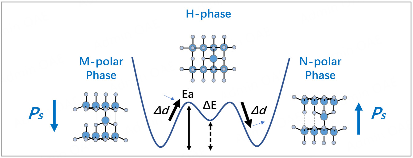
Figure 9. Schematic energy landscape of AlN during the polarization switching via the H-phase transition[30].
Importantly, the H-phase transition has not been experimentally demonstrated in AlN. Thermodynamic analyses indicate a significant energy barrier to achieving this phase under equilibrium conditions. To validate this hypothesis, non-equilibrium deposition methods such as molecular beam epitaxy or pulsed laser deposition under high strain could potentially stabilize the H-phase. In situ techniques - such as TEM under applied electric fields or synchrotron X-ray diffraction during polarization switching - could directly capture transient hexagonal intermediates. Additionally, ultrafast spectroscopy (e.g., pump-probe XRD) might be employed to detect short-lived H-phase states during switching. Findings by Zhang et al.[52] report a marked reduction in the c/a ratio within the Sc concentration range of 0.5 to 0.625, corresponding to an increase in the u parameter. At x = 0.5625, the c/a ratio stabilizes near 1.35, while u approaches 0.45. Within this compositional window, the hexagonal phase exhibits enhanced thermodynamic stability compared to rocksalt structures. This stability is attributed to partial ionic screening, where Sc 3d electrons hybridize with N 2p orbitals, lowering the system's energy. However, as the composition increases beyond x ≥ 0.625 - approaching h-BN-like characteristics with u ≈ 0.5 - the energetic preference shifts back toward the rocksalt phase. While the polar-to-nonpolar phase transition in this regime remains speculative, theoretical predictions suggest that h-BN-like ScN could exhibit ferroelectricity under (0001)-oriented strain. Nonetheless, two key challenges hinder the synthesis of metastable h-BN ScN. First, its formation energy (~0.32 eV per formula unit) is significantly higher than that of the stable rocksalt phase. Second, its realization would require considerable in-plane strain (3%-7%), adding strain energy costs of approximately 0.08-0.21 eV per formula unit. This combination renders the h-BN phase unstable and difficult to achieve in practice. Consequently, for Sc concentrations above x = 0.625, the energetically preferred structure reverts to the rocksalt phase, underscoring the complex relationship between composition and phase stability in Sc-based nitrides.
In (AlN)n/(ScN)m superlattices (SLs), increasing the ScN fraction (x) to 0.5 results in anisotropic lattice expansion: the lattice constants aSL and cSL increase by 5.8% and 5.5% respectively, due to interface strain[30]. In contrast, the solid solution (SS) displays a less consistent trend - cSS shows no monotonic change with x, while aSS increases more significantly, by 7.6% at x = 0.5. The nearly constant c/a ratio in the SL, compared to its decrease in the SS, suggests that strain gradients in the SL may help stabilize the H-phase. Experimental validation using cross-sectional TEM combined with atomic-scale EELS/EDS mapping could resolve local strain fields and hexagonal motifs.
Reconciling structural flattening and Sc-N bonding perspectives
The ferroelectric switching barrier (Ea) shows a significant reduction with increasing x. Specifically, Ea decreases by 66% for SL, while only by 5% for SS, compared to AlN at x = 0.5. This stark contrast suggests that interface-driven strain gradients in SLs, rather than bulk compositional changes in SS, are critical for H-phase stabilization. Therefore, the reduction in Ea cannot be solely attributed to atomic structure flattening. The coordination instability associated with ScN in the wurtzite structure must also be factored in, as it indicates localized structural instability. In contrast, the rocksalt phase of ScN represents a more stable configuration due to its octahedral bonding, while wurtzite ScN remains inherently unstable. This instability is critical in narrowing the energy gap between the wurtzite and hexagonal phases, thereby lowering the switching barrier, since polarization switching proceeds via the H-phase transition. This study emphasizes a crucial reduction in activation energy (Ea) linked to structural instability in both SL and SS systems. Analysis of the energy difference (ΔE) between the wurtzite and hexagonal phases of Al1-xMxN reveals a dependence on the dopant M, which becomes particularly pronounced at higher concentrations. These findings underscore the importance of selecting a dopant with an inherently unstable wurtzite structure, as this effectively lowers both ΔE and Ea in Wurtzite-(Al, M)N systems. Moreover, for M = Sc, spontaneous polarization decreases markedly with increasing x.
Yazawa et al. provide a key perspective, emphasizing the role of Sc-N chemical bond dynamics over simplistic structural flattening arguments (i.e., changes in the c/a ratio)[81]. Their electron localization function (ELF) analysis demonstrates that Sc doping reduces charge localization at Al-N bonds, facilitating easier dipole reorientation. This behavior results from a transition from covalent Al-N bonding - dominated by directional sp3 hybridization - to more ionic, non-directional Sc-N interactions involving sd3 hybridization. The increased bond ionicity at higher Sc concentrations lowers the Peierls-Nabarro barrier for domain wall motion, facilitating polarization reversal. DFT calculations further reveal that Sc substitution contracts in-plane Al-N bonds by 0.05 Å while elongating out-of-plane bonds by 0.12 Å. This distortion creates local h-BN-like motifs that act as nucleation sites for polarization reversal. Yazawa’s work shows that even at low Sc concentrations (observed across a range of compositions, 0 < x < 0.35, and thicknesses of 140-260 nm), the local chemical environment - particularly the ionic character of Sc-N bonds - dictates the energy landscape for switching, independent of global lattice parameter trends. Combinatorial thin films of Al1-xScxN demonstrate a significant reduction in both the coercive field and spontaneous polarization as Sc content increases. This trend mirrors that observed in homogeneous films, where variations in the c/a ratio correlate with changes in the Sc ratio. A pure wurtzite phase is retained for Sc concentrations below 0.35, while a mixed phase emerges beyond this threshold. This transition from a pure wurtzite to a mixed phase aligns with the findings of Satoh et al.[74]. However, the variation in lattice parameters observed here indicates a more invariant c/a ratio with composition than previously reported. These changes in lattice parameters - and the Sc concentrations at which phase transitions occur - are influenced by factors such as the choice of seed layers and underlying metal layers. Such effects can be attributed to stochastic interactions within the Al-Sc subsystem of the broader Al-Sc-N system. Ultimately, the system’s dynamics are governed by interactions between the dopant and host atoms. Notably, changes in the Al-Sc system with increasing Sc concentrations show parallel trends in alloy lattice parameters, particularly the c lattice parameter [Table 1 and Figure 10], consistent with the observations of Satoh et al.[74] and Petrich et al.[75]
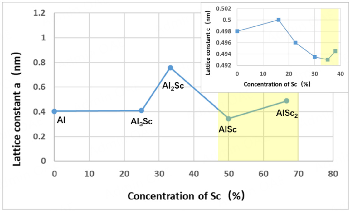
Figure 10. Sc concentration dependence of the lattice constant a in the Sc-Al Structure. A similar variation in parameter a is observed, consistent with trends in the c lattice parameter of the Al1-xScxN structure.
Al-Sc lattice parameter data
While earlier studies by Akiyama et al.[60] and others attributed polarization switching primarily to macroscopic structural flattening (i.e., a reduction in the c/a ratio), Yazawa’s findings complicate this narrative by highlighting the dominant role of local chemical interactions. However, these perspectives are not mutually exclusive. Structural flattening provides a macroscopic framework for understanding phase stability and lattice distortion, which creates favorable conditions for switching. In parallel, Yazawa’s work underscores that the ionic nature of Sc-N bonds governs the microscopic energy barriers for domain wall motion. This distinction is approximately reflected in their relevance across different Sc concentrations:
• At low Sc concentration (x < 0.2): Local chemical effects dominate. Isolated Sc atoms disrupt the covalent Al-N network, introducing bond frustration and localized ionic regions that lower the energy barrier for switching.
• At intermediate concentrations (0.2 < x < 0.4): Both mechanisms coexist. Structural flattening (c/a reduction) softens the lattice globally, while Sc-N ionic bonds reduce local switching barriers.
• At high concentration (x > 0.4): Phase segregation and cubic phase nucleation destabilize ferroelectricity, rendering both mechanisms less effective.
Thus, Yazawa’s work does not contradict earlier structural models but rather complements them by revealing atomic-scale drivers of switching that act alongside macroscopic lattice effects. This dual-scale understanding is essential for optimizing the ferroelectric performance of AlScN, as it suggests that both compositional tuning (to enhance bond ionicity) and strain engineering (to control the c/a ratio) are necessary for effective device design.
The origin of ferroelectric behavior in wurtzite structures likely stems from a combination of local chemical and structural effects. Atomic-scale studies of the Al-B-N system highlight the role of transient non-polar configurations in mediating polarization reversal[23]. DFT calculations show that boron doping flattens the energy landscape, enabling the wurtzite lattice to access a metastable antipolar state during switching [Figure 11].
Figure 11. Nudged-elastic-band simulation of polarization reversal pathways for AlN and Al15/16B1/16N. The insets show structural models at specific simulation stages[23].
This intermediate state, characterized by alternating N-polar and Al-polar motifs, resembles inversion domain boundaries observed in non-ferroelectric III-nitrides[87,88]. Real-time DPC-STEM imaging further supports this mechanism, revealing that switching initiates at localized nucleation sites and propagates via domain wall motion. These findings bridge local chemical effects (bond distortion) with global structural dynamics (domain propagation), offering a unified model for ferroelectricity in wurtzite materials. This duality underscores the importance of optimizing doping strategies to balance ionic character (to lower intrinsic energy barriers) and structural flexibility (to accommodate transient states), as exemplified by emerging Al1-x(Sc,B)xN quaternary alloys.
Studies by Skidmore et al.[4] on heterostructures further highlight the role of interfacial strain and electric fields in facilitating switching. DFT calculations indicate that biaxial tensile strain reduces the polarization reversal barrier in AlN by ~ 15%, consistent with prior work on strain-mediated polymorph stabilization in wurtzite structures[23]. Their proposed model suggests that charged domain walls in the ferroelectric layer generate unscreened electric fields (> 100 MV/cm) and elastic distortions at the interface, which transiently destabilize the non-ferroelectric lattice into a metastable, switchable state [Figure 12][22,23].
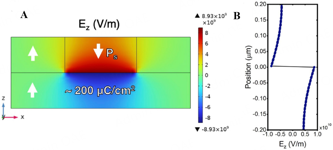
Figure 12. (A) COMSOL simulation of electric field distribution along the z-direction in a ferroelectric slab with a head-to-head domain wall perpendicular to the polar axis, assuming a remanent polarization of 100 μC/cm2. The field concentrates at the wall. (B) Line scan at the center of the domain wall shows a peak electric field of 100 MV/cm, assuming full polarization is maintained to the wall edge[4].
These results align with observations in AlN/AlScN heterostructures, where interfacial domain propagation enables collective switching without chemical substitution[22]. This mechanism is reminiscent of behavior in perovskite heterostructures, where interfacial electric fields modulate polarization[89], but differs by leveraging the low permittivity of nitrides to sustain high field concentrations without dielectric breakdown.
Polarization switching mechanisms
The polarization switching mechanism in Al1-xScxN involves a nuanced interplay between structural evolution and local chemical bonding. While earlier studies attributed the reduced switching barrier primarily to structural flattening (i.e., a reduction in the c/a ratio), recent analyses reveal that the nature of Sc-N chemical bonds plays an equally critical role. This dual influence - structural and electronic - creates a multi-scale mechanism, wherein macroscopic lattice distortions enable polarization reversal, while localized ionic bonding at Sc sites governs the energy landscape of the switching process. Direct evidence of this synergy is provided by in situ STEM imaging of Al0.94B0.06N, where polarization reversal is mediated by a transient non-polar state [Figure 5A].
Ye et al.[30], using ab initio calculations, propose that local structural instabilities induced by Sc doping dominate over bulk lattice flattening in reducing the switching barrier. Their findings align with experimental observations showing that the reduction in coercive field correlates more strongly with Sc-N bond ionicity than with trends in the c/a ratio. For instance, at x = 0.25 Sc, the c/a ratio remains nearly unchanged, yet Ec decreases by ~40%, suggesting that bond-level effects drive the switching dynamics even before significant structural flattening occurs. The transient non-polar state observed in Al-B-N systems mirrors the hypothesized H-phase pathway in Al-Sc-N, suggesting a potentially universal switching mechanism in wurtzite ferroelectrics [Figure 5B]. Further support comes from Keisuke Yazawa’s ELF analysis, which demonstrates that Sc substitution disrupts the sp3 hybridization of Al-N bonds and replaces them with non-directional ionic Sc-N interactions[81]. These weaker directional constraints reduce the energy required for bond reorientation during polarization reversal, even in the absence of pronounced lattice flattening. This transition from covalent to ionic bonding reduces the Peierls-Nabarro barrier for domain wall motion, facilitating polarization reversal. However, structural flattening remains relevant at higher Sc concentrations (x > 0.3), where Sc-induced lattice expansion lowers the energy barrier between polarization states. DFT calculations reveal significant differences in Al-N and Sc-N bond lengths, attributed to the disparity in ionic radii between Al and Sc, as well as the unfavorable tetrahedral coordination of Sc3+. Even at low concentrations, Sc substitution exerts localized effects on Al-N bond lengths - contracting basal-plane bonds while elongating out-of-plane bonds. These changes are consistent with a local structure approaching the 6/mmm hBN-like symmetry, indicative of a non-polar intermediate state during switching in the wurtzite ferroelectric system[46,34]. Accordingly, Sc doping produces two simultaneous effects: (1) local ionic bonding reduces the covalent stiffness of the lattice, facilitating easier bond rotation; and (2) extended lattice distortion - manifested as an increased u parameter and basal plane expansion - stabilizes intermediate states such as the hypothetical H-phase.
These processes are synergistic rather than contradictory. At low concentrations (x < 0.2), ionic bonding dominates the switching mechanism, as evidenced by ELF maps showing isotropic charge distributions around Sc atoms even in minimally distorted lattices[81]. At higher concentrations (x > 0.3), structural flattening further amplifies the effect by reducing steric hindrance to polarization rotation. This explains the nonlinear acceleration of Ec reduction with increasing Sc content: bond ionicity establishes the foundational mechanism, while lattice distortion further lowers the activation energy.
The role of the H-phase transition exemplifies this synergy. While structural flattening (c/a ~ 1.35) theoretically stabilizes the H-phase, successful switching through this pathway depends critically on the Sc-N bond’s ability to accommodate metastable hexagonal coordination - a property absent in pure AlN due to its rigid covalent network. DFT studies confirm that Sc-doped systems exhibit smaller energy differences
Thickness-dependent ferroelectric properties
Thickness scaling is critical for integrating Al1-xScxN into CMOS-compatible devices. Recent breakthroughs in sputter-deposited Al0.72Sc0.28N films have demonstrated robust ferroelectricity at thickness as low as
Divergent thickness-dependent Ec trends have emerged across different growth methods and interfacial conditions. The coercive field and remnant polarization of Al1-xScxN exhibit thickness-dependent behavior that is strongly influenced by interfacial chemistry and strain states. Wang et al.[91] systematically investigated the thickness scaling of MBE-grown Al0.7Sc0.3N films on Mo (011), revealing anomalous Ec behavior in ultrathin layers (5-100 nm). Although classical models predict Ec ∝ d-2/3, Ec increased disproportionately in the 5 nm film due to two main factors:
• Surface oxidation: A 1 nm native oxide layer formed post-growth introduced trapped charges that pinned polarization.
• Compressive strain: Epitaxial mismatch with the Mo substrate induced in-plane compressive strain, distorting the wurtzite lattice and raising the energy barrier for switching.
Notably, the oxide layer modulated the interfacial energy barrier, enabling robust ON/OFF ratios (> 103) and retention even with a reduced remnant polarization (Pr ~ 23 µC/cm2) in 5 nm films.
This behavior stands in stark contrast to that observed by Schönweger et al.[6], where the native oxide on Si acted as a charge reservoir, enabling low-voltage switching and resulting in a reduced Ea in sub-5 nm
Key mechanistic distinctions
Wang et al.[91] (oxide/ferroelectric interface): Trapped charges at the oxide interface amplified polarization pinning, overriding the expected thickness-dependent decrease in Ec.
• Schönweger et al.[6] (ferroelectric/Si interface): The native oxide layer compensated depolarization fields, allowing Ec to scale inversely with thickness.
• Zheng et al.[7] (sputtered films): Tensile strain due to lattice mismatch was the dominant factor affecting switching behavior with decreasing thickness.
Furthermore, Schönweger et al.[6] reported a thickness-dependent increase in relative permittivity (εr), rising from ~ 14 in 100 nm to ~ 18 in sub-5 nm films. This was attributed to domain wall proliferation during electrical cycling. The study underscored the critical role of substrate-induced strain in modulating ferroelectric properties - specifically, the thermal tensile strain on Si substrates (εthermal ≈ 0.09%) vs. the compressive strain observed on sapphire - reinforcing mechanisms previously documented in strained AlScN films[73].
Local coordination and chemical bonding analysis
A significant study by Cohen et al. elucidates the local configurational environment of dopant elements (Sc or Y) in AlN films[14]. In the interaction between nitrogen and aluminum, the 2s and 2p orbitals of N hybridize with the 3s and 3p orbitals of Al, resulting in sp3 hybridization and establishing a tetrahedral coordination typical of the hexagonal wurtzite structure. In contrast, Sc interacts with N through its 3d and 4s orbitals, facilitating octahedral coordination characteristic of the cubic rocksalt structure. The 3d electrons of Sc participate in sd3 hybridization with the 2p orbitals of N, lowering the energy of octahedral sites relative to tetrahedral ones. When aluminum nitride is alloyed with scandium nitride, a strong competition arises between their distinct bonding geometries: tetrahedral Al-N bonds favor sp3 hybridization, while octahedral Sc-N bonds involve sd-sp interactions. These contrasting coordination preferences between the tetrahedral AlN phase and the octahedral ScN phase are pivotal to the structural characteristics of Al1-xScxN alloys. Experimental studies investigating varying Sc content (specifically at
Metal-doped AlN
As previously discussed, the ferroelectric properties of the material are influenced by local structural interactions, specifically the atomic interactions governed by the ratio of the doping metal. This enhancement in switchability has significant implications for non-volatile memory technologies. In this section, we examine the effects of metal doping on AlN and other wurtzite-structured materials in the context of polarization switching.
Polarization switching is based on the potential for polarity inversion - a critical feature that can determine the switching mechanism. Understanding the polarization inversion process is therefore essential for revealing the underlying phenomena. Anggraini et al.[15] demonstrated that doping AlN with Si and MgSi facilitates a transition from Al-polar to N-polar configurations. Thin films typically exhibit Al-polar characteristics at low doping concentrations (less than 1%), with no significant change in the piezoelectric coefficient d33. However, as the doping concentration increases to 1-15 at%, a negative d33 value emerges, indicating a predominance of N-polar orientation. For Si concentrations above 15 at%, a gradual decline in d33 is observed. Undoped AlN typically consists of nanoparticles ranging from 15 to 35 nm in size and predominantly shows Al-polar characteristics. In contrast, the particle size of Si0.11Al0.89N increases to
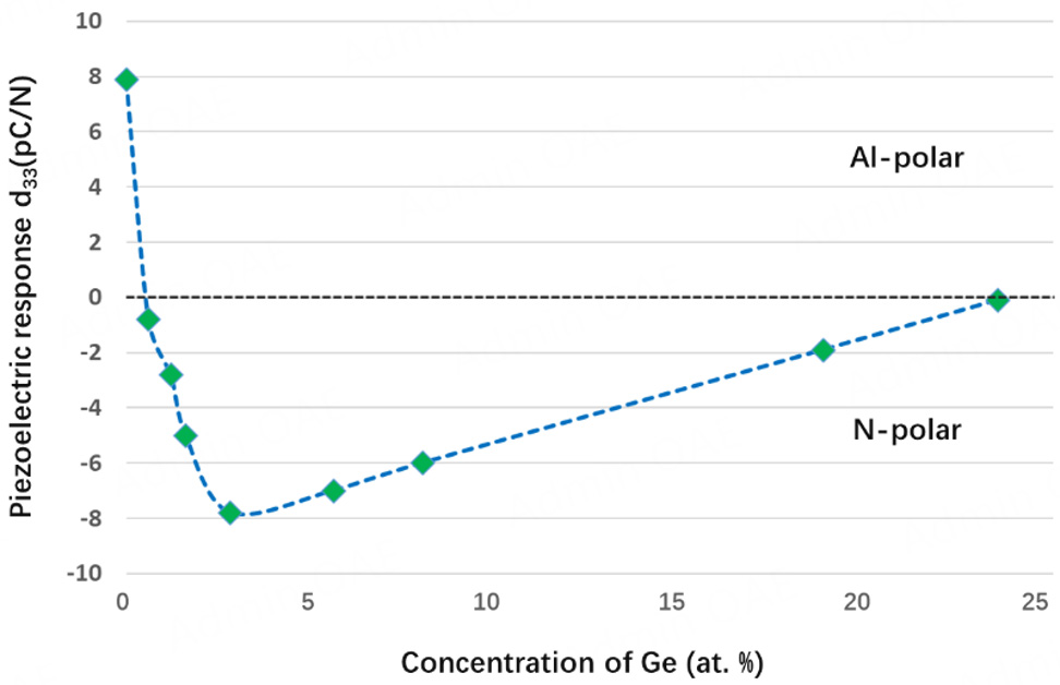
Figure 13. Dependence of the piezoelectric coefficient d33 on Ge concentration in GexAl1-xN thin films. (Reproduced from Ref.[95]).
For instance, the d33 values are approximately -1 and -5.4 pC/N for 0.8 at% Ge and 1 at% Si, respectively. The most pronounced negative d33 value, -6.3 pC/N for Si, corresponds to a transition from approximately +6.8 pC/N (N-polar polarization) observed at two different doping levels: 0.03 and 0.11. Si and Ge exhibit similar oxidation states (+1, +2, +3, +4), as well as comparable electronegativities and atomic radii, which likely accounts for their analogous effects in facilitating polarity inversion. This correlation reinforces the link between ferroelectric behavior and the choice of dopant element, as well as its influence on local atomic interactions. Notably, the asymmetry between the maximum negative and positive d33 values may be attributed to differences in electronegativity. The role of aluminum vacancies in polarity inversion can be interpreted through the formation of a defect complex, denoted as [VAl + nSiAl], which may induce a transition in Si coordination from tetrahedral to octahedral geometry, resulting in the formation of IDBs. Additionally, codoping AlN with Mg and Si shows that when the Mg/Si ratio exceeds 1, d33 adopts a positive value, indicating a predominantly Al-polar thin film. Conversely, when the ratio is below 1, d33 becomes negative, corresponding to a primarily N-polar structure. The observed positive d33 value of 6 pC/N can be attributed to the oxidation states of Mg (+1, +2), which help compensate for the Al vacancies introduced by Si doping. At a Mg/Si ratio of 1, the d33 values are similar to those of undoped AlN films. The influence of codoping on local interactions is further evident from changes in particle size in Mg/Si codoped AlN films. For example, at a Mg/Si ratio of 0,4, particle sizes range from 40 to 80 nm, indicating a predominantly N-polar orientation. In contrast, a ratio greater than 1 results in a different morphology, with particle sizes ranging from 40 to 120 nm. Crystal structure analysis reveals a slight lattice contraction with increasing Si concentration, consistent with N-polar characteristics, while higher Mg concentrations lead to lattice expansion, reflecting Al-polar behavior. According to Anggraini and Takaaki Mizuno, elements with chemical characteristics similar to Si or Ge can induce ferroelectric behavior when doped into AlN, although variations in effect may arise due to differences in electronegativity and atomic radius. Zhu et al.[38] demonstrated a polarization wake-up process for ferroelectric switching in epitaxial Al0.93B0.07N films grown on W-coated c-axis-oriented Al2O3 (sapphire) substrates. Doping AlN with 7 at% B stabilizes the as-deposited film in an N-polar state, as evidenced by rapid KOH etching of N-polar surfaces, which leaves behind residual grains and exposes the underlying tungsten substrate. Initial polarization cycling at
The crystalline asymmetry of the wurtzite structure, characterized by its polar surfaces (e.g., AlN(0001) and AlN(000-1)), plays a critical role in both polarization dynamics and thermal dissipation. Thermal analysis reveals that B-doped AlN maintains a high thermal conductivity (~ 12 W/m K), comparable to undoped AlN and superior to Sc-doped AlN (< 9 W/m k[96]), where increased lattice distortion enhances phonon scattering. However, localized heating at polar interfaces during electrical cycling induces transient temperature spikes (~11 K), which accelerate nitrogen vacancy (VN) migration toward domain walls and polar surfaces[37]. Over time, VN aggregation at these interfaces degrades polarization retention and increases leakage currents, as confirmed by impedance spectroscopy, which shows a tenfold increase in conductivity in fatigued films. This leakage is further exacerbated by oxygen impurities (ON) at the electrode interfaces, which artificially elevate the apparent polarization prior to dielectric breakdown. The choice of electrode material significantly affects endurance: Pt top electrodes withstand ~ 104 cycles, whereas tungsten electrodes extend device lifetimes to ~ 105 cycles due to lower resistivity and reduced Joule heating. Finite element simulations confirm that electric field crowding at electrode edges accelerates dielectric breakdown; however, this can be mitigated through field plate designs (e.g., SU-8 dielectrics with Pt guard rings), which homogenize the electric field distribution and extend endurance up to ~ 106 cycles. The interplay between polarization-induced field stress and thermal dissipation highlights the need for strategic substrate selection (e.g., sapphire for thermal stability) and interfacial engineering to suppress defect migration.
In boron-doped AlN, the polarization reversal process is ultimately nucleation-limited. As-deposited films crystallize in a polar phase with a uniform -Pr orientation and minimal domain wall density, which explains the initially low hysteresis. During early cycling, stable nuclei of oppositely polarized domains form once the applied electric field exceeds the critical threshold (E > Ec), while subsequent cycles promote domain wall motion and domain retraction. Complete volume switching requires achieving a critical density of nucleation sites, as domain wall propagation is spatially constrained during each cycle. This mechanistic framework underscores the importance of defect engineering and thermal management in optimizing wurtzite ferroelectrics for high-endurance applications such as non-volatile memory and piezoelectric sensors.
Tagantsev critiques the characterization of spontaneous polarization as a bulk property[97]. Posternak et al.[98] highlighted the challenges of evaluating spontaneous polarization in BeO under periodic boundary conditions. Martin further argued against deriving such polarization properties from unit cell calculations, citing intercellular charge transfer interactions and the influence of surface states[99]. In contrast,
Doping AlN with Sc has been shown to induce ferroelectric behavior, with both the response and quality of the hysteresis loop being dependent on the Sc content. Therefore, a comparative analysis of Sc doping effects in AlN vs. other related films is critical. Uehara et al.[104] demonstrated ferroelectric behavior in
For Sc concentrations of 0.41 and 0.44, remanent polarization saturation remained consistent across all measurement temperatures but varied with electric field strength. Notably, for x = 0.41 at 473 k and
In the context of polarization switching, several key factors govern the effects of metal doping in AlN and related wurtzite structures:
• Type of metal dopant: Different dopants have markedly different effects on ferroelectric properties. For example, Sc-doped AlN shows enhanced remanent polarization and reduced coercive fields compared to AlN doped with Mg or Zn.
• Dopant concentration: Increasing dopant concentration typically enhances remanent polarization and reduces coercive fields; however, excessive doping can negatively impact ferroelectric behavior.
• Crystal structure: The underlying crystal structure is critical. Sc doping maintains the wurtzite structure favorable for ferroelectricity, while Mg doping tends to result in a zinc blende structure, which is less conducive.
Additional nuances include:
• The effects of metal doping on polarization switching vary among different wurtzite structures.
• Dopant concentration continues to play a key role in determining ferroelectric properties.
• Material defects introduced by doping also influence ferroelectric behavior.
Notably, doping AIN with metals such as Mg, Zn, and Y has shown positive effects on polarization switching. Generally, dopants with a larger ionic radius than Al reduce the coercive field. Conversely, Ga doping tends to increase Ec due to the additional positive charge, which hinders polarization switching. Table 2 summarizes the relationship between atomic radius and electronegativity of the dopant and substituted atoms. A lower electronegativity generally correlates with a larger ionic radius, while a higher electronegativity results in a smaller radius. Understanding this correlation may aid in optimizing ferroelectric performance in wurtzite structures.
Relationship between the atomic radius and electronegativity of dopant and substituted elements
| Element | Electronegativity | Atomic radius (pm) | Covalent radius (pm) | Van der Waals radius (pm) |
| Al | 1.61 | 143 | 121 ± 4 | 184 |
| Sc | 1.36 | 162 | 170 ± 7 | 211 |
| Zn | 1.65 | 134 | 122 ± 4 | 139 |
| Mg | 1.31 | 160 | 141 ± 7 | 173 |
| Ga | 1.81 | 135 | 122 ± 3 | 187 |
| Sc | 1.36 | 162 | 170 ± 7 | 211 |
| Al | 1.61 | 143 | 121 ± 4 | 184 |
| B | 2.04 | 90 | 84 ± 3 | 192 |
The study by Momida et al.[40] further supports this trend, demonstrating notable enhancements in the piezoelectric constants of ABN through the substitution of Al, Ga, and In with Sc, Y, and La - elements characterized by larger atomic radii and lower electronegativity[40].
Exploring the relationship between electronegativity and atomic radius offers promising directions for engineering dopants to improve the polarization-switching characteristics of wurtzite structures. In particular, dopants with lower electronegativity and larger atomic radii have been shown to effectively reduce the coercive field. Ongoing research underscores the importance of this correlation in precisely tuning the ferroelectric properties of wurtzite materials.
Although factors such as material defects and temperature also influence the ferroelectric behavior of doped AlN and related wurtzite structures, the type and concentration of the metal dopant, along with the intrinsic crystal structure, are the most critical determinants. Table 3 summarizes the effects of various metal dopants on the ferroelectric properties of AIN. Notably, Sc-doped AlN exhibits the highest remanent polarization and the lowest coercive field, whereas Zn-doped AlN shows the opposite trend, with the lowest remanent polarization and the highest coercive field.
Effects of different metal dopants on the ferroelectric properties of AlN
| Metal dopant | Remanent polarization (μC/cm2) | Coercive field (MV/cm) |
| Sc | 110 | 1.5 |
| Mg | 85 | 4.5 |
| Zn | 60 | 9 |
ALD OF DOPED ALN: A PROMISING FUTURE
Al1-xScxN alloys have emerged as key materials for advanced ferroelectric and piezoelectric applications due to their exceptional electric breakdown strength (ranging from 2 to 5 MV/cm), which enables the use of thinner ferroelectric layers in memory devices without compromising the memory window. However, integrating these materials into low-voltage systems remains challenging, despite their improved polarization stability and retention at elevated temperatures. Key hurdles include achieving phase purity, minimizing oxygen contamination (due to the high oxygen affinity of Al and Sc, which necessitates a high-vacuum environment during AlScN growth), and maintaining high crystal quality while ensuring industrial scalability. Although deposition techniques such as sputtering, MOCVD, MBE, and PLD have contributed to the advancement of AlScN growth, each method has inherent limitations in terms of defect density, film uniformity, or scalability. In this context, Atomic Layer Deposition (ALD) offers a transformative approach, providing atomic-level precision, CMOS compatibility, and conformal coating capabilities - features that are critical for next-generation devices.
Sputtering: scalability vs. microstructural defects
Sputter deposition is a widely used method for producing Al1-xScxN films with strong c-axis orientation, employing either Al/Sc alloy targets or dual-metal co-sputtering. While alloy targets improve deposition rates and composition uniformity, co-sputtering allows for tunable Sc concentration, albeit often at the expense of film homogeneity. In a pioneering study, Akiyama et al.[60] demonstrated the epitaxial growth of AlScN via reactive RF dual magnetron sputtering on Si (001) substrates. Subsequent research has confirmed the successful growth of c-axis-oriented (0001) AlScN films using reactive magnetron co-sputtering on both silicon and sapphire substrates. However, sputtered films often contain trace amounts of oxygen and suffer from difficulties in achieving a uniform in-plane orientation. This typically results in columnar growth with high threading dislocation densities at grain boundaries, complicating efforts to obtain high crystal quality. These challenges increase the likelihood of defects such as abnormally oriented grains, stemming from the alloy's multiple phases. Controlling the Sc content via alloy targets involves complex metallurgical processes, which can drive up production costs. Co-sputtering offers a more economical alternative, allowing Sc concentration to be tuned by adjusting the power of individual targets. However, this approach may compromise film uniformity and crystallinity. To meet the demands of low-power memory applications and ensure CMOS compatibility, the deposited films must support low-voltage operation and enable low-temperature growth on Si substrates.
Despite these challenges, Liu et al.[48] reaffirmed the feasibility of sputtering for BEOL-compatible AlScN[48]. Their process, conducted in a PVD system without vacuum interruption, achieved excellent reproducibility, with thickness variation within ±1 nm, at CMOS-compatible temperatures (< 350 °C). Furthermore, the use of KOH wet etching for patterning Al electrodes aligns well with standard industrial workflows. These findings highlight sputtering’s continued relevance for scalable, low-cost production of ultra-thin ferroelectric films, complementing ALD’s advantages in conformal coating.
MOCVD: high growth rates vs. precursor limitations
MOCVD has become the method of choice for the large-area, uniform growth of nitride semiconductors, primarily due to its high growth rates (up to several microns per hour) compared to MBE. However, a key challenge facing MOCVD is the limited availability of effective scandium precursors with sufficiently high vapor pressure - a limitation rooted in scandium's classification as a group III-B transition metal. Historically, the low vapor pressure of available precursors has restricted Sc incorporation to doping-level concentrations only[61,106]. Recent developments have introduced scandium precursors with high vapor pressures, representing a significant advancement in this domain. Notably, the Cp3Sc precursor has been utilized in studies that systematically vary parameters such as growth temperature, growth mode, III/V ratio, and reactor pressure to optimize growth conditions[107-109]. Despite these improvements, growth rates using Cp3Sc remain low (~0.006 nm/s), resulting in prolonged thermal exposure and increased interfacial diffusion.
Molecular beam epitaxy (MBE) enables the growth of single-crystalline Al1-xScxN under ultra-high vacuum (approximately 10-10 torr). Early research relied on sputter deposition methods, which typically produced polycrystalline films with textured surfaces[110]. However, recent advancements in MBE have enabled the fabrication of ferroelectric AlScN and GaScN thin films with single-crystalline quality[91,111-114]. These high-quality films have facilitated device miniaturization down to ~5 nm and supported the development of various ferroelectric devices, including ScAlN/GaN heterostructure memories, ScAlN/GaN HEMTs, and ScAlN-based self-powered photodetectors[111,115]. The MBE process involves directing atomic or molecular beams from solid sources of group III elements (Al, Ga, In, Sc) onto a heated substrate. Crucible temperature controls the vapor pressure of each element. In this molecular regime, the evaporated atoms experience minimal collisions before reaching the substrate. A significant breakthrough was reported in 2017 when researchers successfully grew single-crystal AlScN on GaN using radio-frequency plasma-assisted MBE. Their findings showed that metal-rich growth conditions influence phase purity by promoting the formation of intermetallic compounds. Nitrogen is introduced via radical-generating sources or through thermal cracking of ammonia (NH3) on the substrate. Sufficient nitrogen flow is critical for achieving smooth III-nitride films. MBE growth of AlScN typically requires substrate temperatures above 500 °C. In addition to GaN, AlScN epitaxy can be achieved on substrates such as AlN, SiC, Al2O3, and Mo via MBE, MOCVD, or PLD. MBE offers the advantage of producing ultra-thin epitaxial films with high uniformity and the ability to engineer multilayer structures with precisely controlled doping or compositional variations[116]. Nevertheless, MBE suffers from low throughput (~0.1-1 nm/s) and high equipment costs, limiting its viability for industrial-scale applications and confining its use largely to research settings.
By maintaining a substrate temperature of 700 °C and precisely controlling the Sc/Al flux ratio,
PLD: stoichiometric control vs. throughput limitations
PLD offers distinct advantages, particularly its precise stoichiometric transfer from target to substrate, which is essential for stabilizing the metastable wurtzite phase - especially at high Sc concentrations. Recent studies[117] have demonstrated the successful growth of high-quality, single-crystalline ferroelectric Al1-xScxN films using PLD, achieving Sc concentrations up to x = 0.3 while maintaining minimal oxygen contamination (≤ 0.1 at%) and excellent structural integrity. Advanced characterization techniques, including XRD and aberration-corrected STEM, confirmed a domain-matching epitaxial relationship with sapphire substrates, resulting in sharp interfaces and reduced lattice mismatch. These PLD-grown films exhibit impressive properties: a spontaneous polarization of 140 µC/cm2, a fivefold increase in the piezoelectric coefficient (d33 ≈ 10 pm/V) compared to undoped AlN, and ultralow leakage currents
Despite these advantages, conventional PLD faces limitations that hinder industrial scalability, including low deposition rates (~ 0.1 nm/s) and difficulties in achieving uniform coverage over large areas. To overcome these barriers, future research must prioritize three key areas: (1) defect control using in-situ metrology and machine learning-driven process optimization; (2) enhancement of phase stability through predictive doping strategies; and (3) functional device demonstrations (e.g., ferroelectric FinFETs, ultra-wideband RF filters) to validate performance in real-world environments. Addressing these challenges could enable PLD-grown AlScN to realize its full potential in applications such as neuromorphic computing, 6G communications, and high-temperature MEMS, firmly establishing its role in next-generation semiconductor technologies.
AlScN microstructure: strongly dependent on deposition conditions
Yang et al.[119] investigated the effect of substrate temperature on the microstructural characteristics of
Overall, these studies underscore that the microstructure of Al1-xScxN films is highly sensitive to deposition parameters, suggesting that their intrinsic properties are tightly linked to the quality of their crystalline structure.
ALD: bridging precision and scalability
The rise of organic flexible substrate electronics has driven the need for low-temperature processing techniques. Concurrently, ongoing trends in device miniaturization and the demand for precise control over film thickness, deposition parameters, and defect density have positioned ALD as a key enabling technology for next-generation semiconductor devices. Van der Wel et al.[122] introduced an innovative approach to area-selective ALD of AlN films. This technique enables AlN to be deposited exclusively on designated regions of a patterned substrate, which is critical for electronic applications requiring selective material placement. The process begins with substrate pretreatment to remove native AlOxNy, facilitating targeted AlN growth. A key factor in this method is the use of distinct surface terminations: sputtered AlN for the growth surface and thermal SiO2 for the non-growth surface. The authors propose that methylation of the non-growth surface with trimethylaluminum (TMA) effectively inhibits AlN deposition in those areas. This strategy may also be applicable to other nitride materials, such as GaN. Their findings represent a promising strategy for the high-precision deposition of AlN thin films.
III-Nitrides, especially AlN, show great promise for use in high-power electronics, optoelectronic devices, sensors, and transistors. However, several challenges remain, including difficulty in nitrogen incorporation, a lack of suitable native substrates, reliance on thick buffer layers, and high deposition temperatures that hinder compatibility with chip fabrication - particularly during Back-End-Of-Line processes. ALD has emerged as a viable alternative for next-generation III-Nitride applications, enabling the growth of sub-10 nm films through surface-controlled precursor reactions. This method allows for conformal coating of complex geometries with exceptional thickness control and uniformity across large areas. ALD-based AlN deposition has been explored for over three decades, typically using TMA as the metal precursor and ammonia (NH3) as the nitrogen precursor, alongside various combinations of nitrogen and aluminum precursors[90,123-127]. Despite efforts to optimize precursor combinations, many reactions still suffer from inefficient stoichiometry, with low nitrogen-to-metal precursor ratios. The high consumption of precursor gases and the accumulation of unreacted nitrogen necessitate additional treatment equipment, increasing system complexity and cost, thus limiting mass-production viability. A key limitation stems from the use of metal-carbon bonded precursors, which complicate ammonia dissociation. To address this, researchers are exploring alternative precursors that directly bond metal and nitrogen atoms, potentially easing ammonia activation. Promising candidates include formamidinates, amidinates, trisguanidinates, and triazenides[128-130]. Seppänen et al.[131] proposed an Atomic Layer Annealing method, applying a 20-second Ar plasma pulse at 200 W after each deposition cycle to improve stoichiometry, crystallinity, and c-axis orientation while reducing carbon and hydrogen impurities. Similarly, Shih et al.[132] achieved high-quality AlN thin films using Plasma-Enhanced ALD (PE-ALD) coupled with in situ Atomic Layer Annealing, transforming amorphous AlN into a single-crystalline epitaxial film at a relatively low deposition temperature of 300 °C. Kao et al.[133] further demonstrated that electron beam annealing can enhance the density of epitaxial AlN layers while minimizing damage, making it suitable for low-temperature deposition. Despite the growing body of research on ALD-deposited AIN, studies on doped AlN remain limited, with fewer than 20 publications in the ALD database addressing doped AlN[134]. Nepal et al.[135], in work on
Tian et al.[136] explored the use of hydrogen plasma to enhance the reactivity between TMA and NH3 precursors. Their study reported very low oxygen and carbon contamination (around 1.5% and 1%, respectively) and fewer C-Al bonds in PE-ALD samples compared to those produced by thermal ALD. This suggests that H2 plasma may aid in breaking Al-CH3 bonds in TMA or increasing the NH3 reactivity. Notably, lower H2 flow rates resulted in polycrystalline films with poor crystallinity, while higher H2 flow rates yielded films with a (002) preferred orientation, contrasting with the (0010) orientation commonly seen in thermal ALD. Ozgit et al.[137] achieved a constant growth rate of 0.86 Å/cycle over the 100 to 200 °C range, even at very low deposition temperatures. Additionally, variations in plasma generation methods - such as direct inductively coupled plasma and indirect capacitively coupled plasma - have been shown to affect AlN growth[138], influencing growth per cycle (e.g., up to 1.54 Å/cycle), total cycle duration, homogeneity, and residual oxygen content. Thus, plasma type and configuration should be carefully considered during process optimization. Optimizing growth conditions - such as substrate temperature, growth pressure, and gas flow rates - is crucial for achieving desired film microstructures, enhancing crystallinity, and minimizing defect densities. Techniques such as high-purity precursors, in situ cleaning, and carefully tuned deposition parameters can contribute significantly to the quality of doped AlN films. The choice between PLD and ALD for doped AlN synthesis hinges on specific application requirements. PLD is ideal for producing high-quality epitaxial films with precise stoichiometry, low oxygen contamination, and excellent thermal stability, making it suitable for high-performance, research-grade devices. ALD, in contrast, excels in providing conformal coatings on complex 3D structures with sub-nanometer thickness control - critical for CMOS compatibility and industrial scalability. However, ALD faces challenges in incorporating refractory dopants like Sc due to precursor limitations and often requires post-deposition annealing, which can degrade film or interface quality. While sputtering, MBE, and PLD have advanced AlScN research, ALD’s unparalleled precision, conformality, and scalability address key challenges in doping control, defect engineering, and process integration. Recent advances in precursor chemistry, plasma engineering, hybrid deposition techniques, and post-processing have begun to address these limitations. As semiconductor technologies continue to scale down and require ultrathin, low-power ferroelectrics, ALD is increasingly seen as a cornerstone of future nitride semiconductor development.
The convergence of ALD’s conformality with PLD’s epitaxial precision may enable the creation of defect-engineered heterostructures for applications such as RF filters and neuromorphic computing. Ultrathin ALD-grown AlScN (< 10 nm) with low leakage current supports low-voltage memory applications, while low-temperature deposition on flexible substrates opens the door to wearable sensors. Scalable methods such as multi-target PLD and HT-PLD, combined with ALD’s atomic-level control, position doped AlN at the forefront of high-frequency resonators, self-powered photodetectors, and haptic interface technologies.
Table 4 summarizes the advantages and disadvantages of various thin-film growth methods, including Magnetron Sputtering, MBE, ALD, and PLD.
Advantages and disadvantages of common thin-film deposition methods
| Feature | Magnetron sputtering | Molecular beam epitaxy (MBE) | Atomic layer deposition (ALD) | Pulsed laser deposition (PLD) |
| Typical growth temp. | Low to moderate (< 400 °C possible) | Moderate to high (Often > 600 °C) | Low to moderate (Often 200-400 °C) | Moderate to high (Substrate heating required) |
| Film quality | Good Polycrystalline (textured films possible) | Excellent epitaxial/single-crystal | Variable (from amorphous to polycrystalline) | Good epitaxial/polycrystalline films possible |
| Purity | Good (depends on target purity) | Very high (UHV environment) | Variable (depends on precursor purity/residues) | Good (Stoichiometric transfer possible) |
| Uniformity | Good (suitable for large-area deposition) | Moderate (requires substrate rotation for uniformity) | Excellent | Moderate (Can be challenging over large areas) |
| Scalability/throughput | High | Low | Moderate (Batch processing possible) | Moderate (Combinatorial approaches possible) |
| Conformality | Low to moderate | Low | Excellent | Low to moderate |
| CMOS compatibility | High (Low temp., BEOL integration possible) | Moderate (higher temp.) | High (Low temp., BEOL integration possible) | Moderate (temp. and particulates are concerns) |
| Key advantages | Scalable, CMOS-compatible, widely adopted | Highest quality/purity, Precise control | Conformality, thickness control | Versatile, enables Stoichiometric material transfer |
| Key disadvantages | Limited conformality, potential defects | Slow, expensive, high temp. required | Slow, precursor-related challenges, variable purity | Particle generation, Uniformity issues |
CONCLUSIONS
Metal doping has emerged as a promising strategy to enhance the polarization-switching characteristics of wurtzite AlN thin films. The selection and concentration of dopants can vary among different wurtzite structures and are influenced by inherent material defects. These factors affect film polarity, polarization magnitude, and switching behavior. The proposed polarization-switching mechanisms in wurtzite AlN are closely linked to the dopant species, which significantly influence polarization dynamics. Furthermore, intrinsic material defects can serve as nucleation sites for domain walls, playing a key role in the switching process. Investigations into AlScN and other doped wurtzite materials have revealed complex interactions among structural, chemical, and electronic factors that govern their ferroelectric properties. Critical to this behavior is the local atomic environment, particularly the coordination of Sc and Al atoms, which strongly influences the polarization-switching mechanism. The nature of the chemical bonding, shaped by the dopant’s electronegativity and atomic radius, critically impacts the energy barrier for polarization reversal. Various deposition techniques - such as atomic layer deposition (ALD), molecular beam epitaxy (MBE), and sputtering - offer distinct advantages and limitations in fabricating high-quality AlScN films with tailored properties. ALD, in particular, provides precise control over film thickness and composition, though it may face challenges related to precursor chemistry and slower growth rates. Future investigations should prioritize elucidating the fundamental switching mechanisms, optimizing doping strategies, improving film quality, and developing innovative device architectures. Studies on B-doped AlN suggest promising directions for optimizing wurtzite ferroelectrics. Hybrid doping strategies (e.g., Al1-x-yBxScyN) may combine the low coercive field of Sc with the high thermal stability of B, although miscibility issues remain a challenge. Moreover, device designs such as field plates and ALD-grown encapsulation layers (e.g., Al2O3) could mitigate oxidation and defect migration, potentially extending the operational lifetime of non-volatile memory devices. Future work should explore transient thermal modeling to address self-heating in high-frequency RF devices and investigate combinatorial doping approaches (e.g., B + Y, B + La) to decouple polarization switching from lattice strain. Addressing these challenges, while leveraging the unique properties of AlScN and related doped wurtzite materials, may enable the development of next-generation devices with outstanding performance and reliability. Although the study of metal doping effects on polarization switching in wurtzite AlN is still in its early stages, careful selection of dopant types and concentrations can yield films with optimized polarity, polarization strength, and switching characteristics. Doping with rare-earth elements presents stability challenges, for which ALD may offer a robust solution. Given the high costs of rare-earth elements, researchers such as Startt et al.[18] have recommended using group IVB metals as a more economical alternative.
Table 5 summarizes various Al1-xScxN-based layers with different Sc concentrations fabricated using a range of deposition methods.
Summary of Al1-xScxN-based layers with different Sc concentrations fabricated using various deposition methods
| No. | Unit | Author | Style of deposition | Al-Sc-based system | Thickness | Ratio | Ec | Pr | References |
| 1 | University of Kiel/Germany | Georg Schönweger Simon Fichtner | Sputtering | Al1-xScxN | 5 nm | x = 0.26 | 2.1 MV/cm | - | [6] |
| 2 | Albert-Ludwigs University/Germany | Jana Lig Stefano Leone | MOCVD | Al0.7-xNixSc0.3N | 10 nm | x = 0.14 | - | - | [139] |
| 3 | University of Freiburg/Germany | Kathrin Frei | MBE | Al1-xScxN | 20 nm | x = 0.02-0.69 | - | - | [140] |
| 4 | University of Pennsylvania/USA | Dixiong Wang Roy H. Olsson | Sputtering | Al1-xScxN | 20 nm | x = 0.32 | 6.5 MV/cm | 140 µC/cm2 | [141] |
| 5 | Tokyo Institute of Technology/Japan | Junji Kataoka | Sputtering | Al1-xScxN | 30 nm | x = 0.22 | - | - | [142] |
| 6 | Tokyo Institute of Technology/Japan | Si-Meng Chen | Sputtering | Al1-xScxN | 30-40 nm | x = 0.26 | - | - | [143] |
| 7 | Seoul National University/Republic of Korea | Seung Kyu Ryoo Cheol Seong Hwang | Sputtering | Al1-xScxN | 20 nm 45 nm | x = 0.3 | 6.5 MV/cm (20 nm) 6.0 MV/cm (45 nm) | 60 μC/cm2 (20 nm) 110 μC/cm2 (45 nm) | [144] |
| 8 | University of Pennsylvania/USA | Xiwen Liu Roy H. Olsson Deep Jariwala | Sputtering | Al1-xScxN | 100 nm | x ≥ 0.27 x = 0.29 | 2-4.5 MV/cm / | 80-115 μC/cm2 80 μC/cm2 | [8] |
| 9 | University of Michigan/USA | Ping Wang Ding Wang Zetian Mi | MBE | Al1-xScxN | 100 nm | x = 0.2 | 4.2 MV/cm | 135 µC/cm2 | [145] |
| 10 | University of North Western Industry/China | Bingcheng Luo | Sputtering | Al0.7-yNiySc0.3N | 189 nm | x = 0.3 | 3 MV/cm | 100 μC/cm2 | [146] |
| 11 | Naval Research Laboratory/USA | Matthew T. Hardy | MBE | Al1-xScxN | 200 nm | x = 0.16-0.18 | - | - | [147] |
| 12 | Naval Research Laboratory/USA | Matthew T. Hardy | MBE | Al1-xScxN | 200 nm | x = 0.06-0.32 | - | - | [148] |
| 13 | University of Kiel/Germany | Simon Fichtner | Sputtering | Al1-xScxN | 400 nm | x = 0.27 | 5 MV/cm at x = 0.27(max) | 110 μC/cm2 at x = 0.27(max) | [46] |
| 600 nm | x =0.32/0.36/0.40 | ||||||||
| 1,000 nm | x = 0.43 | ||||||||
| 14 | University of Craiova/Romania | Cosmin Silviu Sandu | Sputtering | Al1-xScxN | 500 nm | x = 0.00-0.43 | - | - | [149] |
| 15 | Georgia Institute of Technology/USA | Jialin Wang | Sputtering | Al1-xScxN | 900 nm | x = 0.3 | 0.2 MV/cm | 80 μC/cm2 | [150] |
| 16 | Fraunhofer Institute for Silicon Technology (ISIT) & University of Kiel/Germany | Tom-Niklas Kreutzer Simon Fichtner | Sputtering | Al1-xScxN | 500 + 500 nm | x = 0.35 | - | - | [151] |
DECLARATIONS
Authors’ contributions
Conceptualization, validation, formal analysis, resources, writing - original draft preparation: Saadi, M.
Visualization: Shao, W.
Project administration: Tong, Y.
Methodology, data curation: Saadi, M.; Shao, W.
Funding acquisition: Wang, X.; Tong, Y.
Writing - review and editing: Saadi, M.; Wang, X.; Tong, Y.
Investigation: Saadi, M.; Han, C.; Zhang, M.; Shao, W.
Supervision: Wang, X.; Zhang, H.; Tong, Y.; Hu, Y.
Methodology, investigation: Qin, H.
All authors have read and agreed to the published version of the manuscript.
Availability of data and materials
Not applicable.
Financial support and sponsorship
This work was funded by the 2030 Major Project of the Chinese Ministry of Science and Technology, grant No. 2021ZD0201200, and the High-End Foreign Expert Team of the Ministry of Science and Technology, grant No. G2022178034L. This work was also supported in part by the research fund of the Suzhou laboratory (No. SK-1202-2024-012).
Conflicts of interest
All authors declared that there are no conflicts of interest.
Ethical approval and consent to participate
Not applicable.
Consent for publication
Not applicable.
Copyright
© The Author(s) 2025.
REFERENCES
1. Yasuoka, S.; Shimizu, T.; Tateyama, A.; et al. Effects of deposition conditions on the ferroelectric properties of (Al1-xScx)N thin films. J. Appl. Phys. 2020, 128, 114103.
2. Lin, B. T.; Lee, W. H.; Shieh, J.; Chen, M. J. Ferroelectric AlN ultrathin films prepared by atomic layer epitaxy, In Proceedings Behavior and Mechanics of Multifunctional Materials XIII; 2019.
3. Hasegawa, K.; Shimizu, T.; Ohsawa, T.; Sakaguchi, I.; Ohashi, N. Full polarization reversal at room temperature in unsubstituted AlN. Appl. Phys. Lett. 2023, 123, 192903.
4. Skidmore, C. H.; Spurling, R. J.; Hayden, J.; et al. Proximity ferroelectricity in wurtzite heterostructures. Nature 2025, 637, 574-9.
5. Kim, K. H.; Han, Z.; Zhang, Y.; et al. Multistate, ultrathin, back-end-of-line-compatible AlScN ferroelectric diodes. ACS. Nano. 2024, 18, 15925-34.
6. Schönweger, G.; Wolff, N.; Islam, M. R.; et al. In-grain ferroelectric switching in sub-5 nm Thin Al0.74Sc0.26N films at 1 V. Adv. Sci. 2023, 10, e2302296.
7. Zheng, J. X.; Fiagbenu, M. M. A.; Esteves, G.; et al. Ferroelectric behavior of sputter deposited Al0.72Sc0.28N approaching 5 nm thickness. Appl. Phys. Lett. 2023, 122, 222901.
8. Liu, X.; Wang, D.; Kim, K. H.; et al. Post-CMOS compatible aluminum scandium nitride/2D channel ferroelectric field-effect-transistor memory. Nano. Lett. 2021, 21, 3753-61.
9. Hu, Z.; Cho, H.; Rai, R. K.; et al. Demonstration of highly scaled AlScN ferroelectric diode memory with storage density > 100 Mbit/mm2. arXiv 2025, 2504.13283.
10. Pradhan, D. K.; Moore, D. C.; Kim, G.; et al. A scalable ferroelectric non-volatile memory operating at 600 °C. Nat. Electron. 2024, 7, 348-55.
11. Dai, X.; Hua, Q.; Jiang, C.; et al. Artificial synapse based on a tri-layer AlN/AlScN/AlN stacked memristor for neuromorphic computing. Nano. Energy. 2024, 124, 109473.
12. Nomoto, K.; Casamento, J.; Nguyen, T. S.; et al. AlScN/GaN HEMTs with 4 A/mm on-current and maximum oscillation frequency >130 GHz. Appl. Phys. Express. 2025, 18, 016506.
13. Zhao, C.; Xu, B.; Wang, Z.; Wang, Z. Boron-doped III-V semiconductors for Si-based optoelectronic devices. J. Semicond. 2020, 41, 011301.
14. Cohen, A.; Li, J.; Cohen, H.; et al. Local environment of Sc and Y dopant ions in aluminum nitride thin films. ACS. Appl. Electron. Mater. 2024, 6, 853-61.
15. Anggraini, S. A.; Uehara, M.; Hirata, K.; Yamada, H.; Akiyama, M. Polarity inversion of aluminum nitride thin films by using Si and MgSi dopants. Sci. Rep. 2020, 10, 4369.
16. Alam, M. N.; Olszewski, O. Z.; Campanella, H.; Nolan, M. Large piezoelectric response and ferroelectricity in Li and V/Nb/Ta Co-doped w-AlN. ACS. Appl. Mater. Interfaces. 2021, 13, 944-54.
17. Yokoyama, T.; Iwazaki, Y.; Onda, Y.; Nishihara, T.; Sasajima, Y.; Ueda, M. Highly piezoelectric co-doped AlN thin films for wideband FBAR applications. IEEE. Trans. Ultrason. Ferroelectr. Freq. Control. 2015, 62, 1007-15.
18. Startt, J.; Quazi, M.; Sharma, P.; et al. Unlocking AlN piezoelectric performance with earth-abundant dopants. Adv. Elect. Mater. 2023, 9, 2201187.
19. Savant, C.; Gund, V.; Nomoto, K.; et al. Ferroelectric AlBN films by molecular beam epitaxy. Appl. Phys. Lett. 2024, 125, 072902.
20. Anggraini, S. A.; Uehara, M.; Yamada, H.; Akiyama, M. Investigating the piezoelectric response of Mg-Ti-doped-AlN thin films for sensor application. 2017 IEEE Sensors, Glasgow, UK, 29 October 2017 - 01 November 2017; pp. 1-3.
21. Eliseev, E. A.; Morozovska, A. N.; Maria, J. P.; Chen, L. Q.; Gopalan, V. Thermodynamic theory of proximity ferroelectricity. Phys. Rev. X. 2025, 15, 021058.
22. Stutzmann, M.; Ambacher, O.; Eickhoff, M.; et al. Playing with polarity. Phys. Stat. Sol. B. 2001, 228, 505-12.
23. Calderon, S.; Hayden, J.; Baksa, S. M.; et al. Atomic-scale polarization switching in wurtzite ferroelectrics. Science 2023, 380, 1034-8.
24. Maria, J. P.; Skidmore, C. Data for "Proximity ferroelectricity in wurtzite heterostructures". Scholarsphere 2024. DOI: 10.26207/qaed-vy98.
25. Drury, D.; Yazawa, K.; Zakutayev, A.; Hanrahan, B.; Brennecka, G. High-temperature ferroelectric behavior of Al0.7Sc0.3N. Micromachines 2022, 13, 887.
26. Zhu, W.; Hayden, J.; He, F.; et al. Strongly temperature dependent ferroelectric switching in AlN, Al1-xScxN, and Al1-xBxN thin films. Appl. Phys. Lett. 2021, 119, 062901.
27. Höglund, C.; Birch, J.; Alling, B.; et al. Wurtzite structure Sc1-xAlxN solid solution films grown by reactive magnetron sputter epitaxy: structural characterization and first-principles calculations. J. Appl. Phys. 2010, 107, 123515.
28. Saha, B.; Saber, S.; Naik, G. V.; et al. Development of epitaxial Al1-xScxN for artificially structured metal/semiconductor superlattice metamaterials: epitaxial AlxSc1-xN for artificially structured superlattice metamaterials. Phys. Status. Solidi. B. 2015, 252, 251-9.
29. Brien, V.; Pigeat, P. Correlation between the oxygen content and the morphology of AlN films grown by r.f. magnetron sputtering. J. Crystal. Growth. 2008, 310, 3890-5.
30. Ye, K. H.; Han, G.; Yeu, I. W.; Hwang, C. S.; Choi, J. Atomistic understanding of the ferroelectric properties of a wurtzite-structure (AlN)n/(ScN)m superlattice. Phys. Rap. Res. 2021, 15, 2100009.
31. Dawber, M.; Chandra, P.; Littlewood, P. B.; Scott, J. F. Depolarization corrections to the coercive field in thin-film ferroelectrics. J. Phys. Condens. Matter. 2003, 15, L393-8.
32. Hayden, J.; Hossain, M. D.; Xiong, Y.; et al. Ferroelectricity in boron-substituted aluminum nitride thin films. Phys. Rev. Mater. 2021, 5, 044412.
33. Ferri, K.; Bachu, S.; Zhu, W.; et al. Ferroelectrics everywhere: ferroelectricity in magnesium substituted zinc oxide thin films. J. App. Phys. 2021, 130, 044101.
34. Moriwake, H.; Yokoi, R.; Taguchi, A.; et al. A computational search for wurtzite-structured ferroelectrics with low coercive voltages. APL. Mater. 2020, 8, 121102.
35. Dai, Y.; Wu, M. Covalent-like bondings and abnormal formation of ferroelectric structures in binary ionic salts. Sci. Adv. 2023, 9, eadf8706.
37. He, F.; Zhu, W.; Hayden, J.; et al. Frequency dependence of wake-up and fatigue characteristics in ferroelectric Al0.93B0.07N thin films. Acta. Mater. 2024, 266, 119678.
38. Zhu, W.; He, F.; Hayden, J.; et al. Wake-up in Al1-xBxN ferroelectric films. Adv. Electron. Mater. 2022, 8, 2100931.
39. Yazawa, K.; Hayden, J.; Maria, J. P.; et al. Anomalously abrupt switching of wurtzite-structured ferroelectrics: simultaneous non-linear nucleation and growth model. Mater. Horiz. 2023, 10, 2936-44.
40. Momida, H.; Teshigahara, A.; Oguchi, T. Strong enhancement of piezoelectric constants in ScxAl1-xN: first-principles calculations. AIP. Adv. 2016, 6, 065006.
41. Messi, F.; Patidar, J.; Rodkey, N.; Dräyer, C. W.; Trassin, M.; Siol, S. Ferroelectric AlScN thin films with enhanced polarization and low leakage enabled by high-power impulse magnetron sputtering. APL. Mater. 2025, 13, 051123.
42. Sun, W.; Zhou, J.; Jin, F.; Liu, N.; Zheng, S.; Li, B. Temperature dependence in coercive field of ferroelectric AlScN integrated on Si substrate, In 2024 IEEE International Conference on IC Design and Technology (ICICDT). Singapore; 2024, pp. 1-4.
43. Hornsteiner, J.; Born, E.; Fischerauer, G.; Riha, E. Surface acoustic wave sensors for high-temperature applications, In Proceedings of the 1998 IEEE International Frequency Control Symposium, 1998; pp. 615-20.
44. Yazawa, K.; Drury, D.; Zakutayev, A.; Brennecka, G. L. Reduced coercive field in epitaxial thin film of ferroelectric wurtzite
45. Tasnádi, F.; Alling, B.; Höglund, C.; et al. Origin of the anomalous piezoelectric response in wurtzite ScxAl1-xN alloys. Phys. Rev. Lett. 2010, 104, 137601.
46. Fichtner, S.; Wolff, N.; Lofink, F.; Kienle, L.; Wagner, B. AlScN: a III-V semiconductor based ferroelectric. J. Appl. Phys. 2019, 125, 114103.
47. Galsin, J. S. Chapter 1 - Crystal Structure of Solids. Solid State Physics. Elsevier; 2019. pp. 1-36.
48. Liu, X.; Zheng, J.; Wang, D.; et al. Aluminum scandium nitride-based metal-ferroelectric-metal diode memory devices with high on/off ratios. Appl. Phys. Lett. 2021, 118, 202901.
49. Wang, J.; Park, M.; Mertin, S.; Pensala, T.; Ayazi, F.; Ansari, A. A high-kt2 switchable ferroelectric Al0.7Sc0.3N film bulk acoustic resonator. In 2020 Joint Conference of the IEEE International Frequency Control Symposium and International Symposium on Applications of Ferroelectrics (IFCS-ISAF), Keystone, CO, USA; 2020, pp. 1-3.
50. Herrera, B.; Pirro, M.; Giribaldi, G.; Colombo, L.; Rinaldi, M. AlScN programmable ferroelectric micromachined ultrasonic transducer (FMUT). In 2021 21st International Conference on Solid-State Sensors, Actuators and Microsystems (Transducers), Orlando, FL, USA; 2021, pp. 38-41.
51. Rassay, S.; Mo, D.; Li, C.; Choudhary, N.; Forgey, C.; Tabrizian, R. Intrinsically switchable ferroelectric scandium aluminum nitride lamb-mode resonators. IEEE. Electron. Device. Lett. 2021, 42, 1065-8.
52. Zhang, S.; Holec, D.; Fu, W. Y.; Humphreys, C. J.; Moram, M. A. Tunable optoelectronic and ferroelectric properties in Sc-based III-nitrides. J. App. Phys. 2013, 114, 133510.
53. Business Research Insights. Thin film piezoelectric devices market size, share, growth, trends and industry analysis, by type (AlN Thin Film, PZT Thin Film), by application (Consumer Electronics, Healthcare, Aerospace and Defense, Others), regional insights and forecast From 2025 to 2033 . Available from: https://www.businessresearchinsights.com/market-reports/thin-film-piezoelectric-devices-market-110756 [Last accessed on 28 Jul 2025].
54. Höglund, C.; Bareño, J.; Birch, J.; Alling, B.; Czigány, Z.; Hultman, L. Cubic Sc1-xAlxN solid solution thin films deposited by reactive magnetron sputter epitaxy onto ScN(111). J. Appl. Phys. 2009, 105, 113517.
55. dos Santos, R. B.; Rivelino, R.; de Brito Mota, F.; Gueorguiev, G. K.; Kakanakova-Georgieva, A. Dopant species with Al-Si and N-Si bonding in the MOCVD of AlN implementing trimethylaluminum, ammonia and silane. J. Phys. D. Appl. Phys. 2015, 48, 295104.
56. Taniyasu, Y.; Kasu, M.; Makimoto, T. An aluminium nitride light-emitting diode with a wavelength of 210 nanometres. Nature 2006, 441, 325-8.
57. Bernardini, F.; Fiorentini, V.; Vanderbilt, D. Spontaneous polarization and piezoelectric constants of III-V nitrides. Phys. Rev. B. 1997, 56, R10024-7.
58. Aubert, T.; Bardong, J.; Legrani, O.; et al. In situ high-temperature characterization of AlN-based surface acoustic wave devices. J. Appl. Phys. 2013, 114, 014505.
59. Aubert, T.; Elmazria, O.; Assouar, B.; Hamdan, A.; Genève, D. Reliability of AlN/Sapphire bilayer structure for high-temperature SAW applications. In 2010 IEEE International Ultrasonics Symposium, San Diego, CA, USA; 2010, pp. 1490-3.
60. Akiyama, M.; Kamohara, T.; Kano, K.; Teshigahara, A.; Takeuchi, Y.; Kawahara, N. Enhancement of piezoelectric response in scandium aluminum nitride alloy thin films prepared by dual reactive cosputtering. Adv. Mater. 2009, 21, 593-6.
61. Deng, R.; Jiang, K.; Gall, D. Optical phonon modes in Al1-xScxN. J. Appl. Phys. 2014, 115, 013506.
62. Jin, E. N.; Hardy, M. T.; Mock, A. L.; et al. Band alignment of ScxAl1-xN/GaN heterojunctions. ACS. Appl. Mater. Interfaces. 2020, 12, 52192-200.
63. Constantin, C.; Brithen, H. A.; Haider, M. B.; Ingram, D.; Smith, A. R. ScGaN alloy growth by molecular beam epitaxy: evidence for a metastable layered hexagonal phase. Phys. Rev. B. 2004, 70, 239902.
64. Moram, M. A.; Zhang, S. ScGaN and ScAlN: emerging nitride materials. J. Mater. Chem. A. 2014, 2, 6042-50.
65. Tholander, C.; Birch, J.; Tasnádi, F.; et al. Ab initio calculations and experimental study of piezoelectric Y In1-N thin films deposited using reactive magnetron sputter epitaxy. Acta. Mater. 2016, 105, 199-206.
66. Umeda, K.; Kawai, H.; Honda, A.; Akiyama, M.; Kato, T.; Fukura, T. Piezoelectric properties of ScAlN thin films for piezo-MEMS devices, In IEEE 26th International Conference on Micro Electro Mechanical Systems (MEMS), Taipei, Taiwan; 2013, pp. 733-6.
67. Liauh, W. J.; Wu, S.; Huang, J. L.; Lii, D. F.; Lin, Z. X.; Yeh, W. K. Microstructure and piezoelectric properties of reactively sputtered highly C-axis ScxAl1-xN thin films on diamond-like carbon/Si substrate. Surf. Coat. Technol. 2016, 308, 101-7.
68. Talley, K. R.; Millican, S. L.; Mangum, J.; et al. Implications of heterostructural alloying for enhanced piezoelectric performance of (Al,Sc)N. Phys. Rev. Mater. 2018, 2, 063802.
69. Furuta, K.; Hirata, K.; Anggraini, S. A.; Akiyama, M.; Uehara, M.; Yamada, H. First-principles calculations of spontaneous polarization in ScAlN. J. Appl. Phys. 2021, 130, 024104.
70. Lu, H.; Schönweger, G.; Petraru, A.; Kohlstedt, H.; Fichtner, S.; Gruverman, A. Domain dynamics and resistive switching in ferroelectric Al1-xScxN thin film capacitors. Adv. Funct. Mater. 2024, 34, 2315169.
71. Tybell, T.; Paruch, P.; Giamarchi, T.; Triscone, J. M. Domain wall creep in epitaxial ferroelectric Pb(Zr0.2Ti0.08)O3 thin films. Phys. Rev. Lett. 2002, 89, 097601.
72. Wang, D.; Wang, D.; Zhou, P.; et al. On the surface oxidation and band alignment of ferroelectric Sc0.18Al0.82N/GaN heterostructures. Appl. Surf. Sci. 2023, 628, 157337.
73. Dreyer, C. E.; Janotti, A.; Van de Walle, C. G.; Vanderbilt, D. Correct implementation of polarization constants in Wurtzite materials and impact on III-nitrides. Phys. Rev. X. 2016, 6, 021038.
74. Satoh, S.; Ohtaka, K.; Shimatsu, T.; Tanaka, S. Crystal structure deformation and phase transition of AlScN thin films in whole Sc concentration range. J. Appl. Phys. 2022, 132, 025103.
75. Petrich, R.; Bartsch, H.; Tonisch, K.; Jaekel, K.; Barth, S.; Bartzsch, H. Investigation of ScAlN for piezoelectric and ferroelectric applications. In 2019 22nd European Microelectronics and Packaging Conference & Exhibition (EMPC), Pisa, Italy; 2019, pp. 1-5.
77. Koh, Y. R.; Shi, J.; Wang, B.; et al. Thermal boundary conductance across epitaxial metal/sapphire interfaces. Phys. Rev. B. 2020, 102, 205304.
78. Milyutin, E.; Harada, S.; Martin, D.; et al. Sputtering of (001)AlN thin films: control of polarity by a seed layer. J. Vac. Sci. Technol. B. 2010, 28, L61-3.
79. Yasuoka, S.; Mizutani, R.; Ota, R.; et al. Tunable ferroelectric properties in Wurtzite (Al0.8Sc0.2)N via crystal anisotropy. ACS. Appl. Electron. Mater. 2022, 4, 5165-70.
80. Farrer, N.; Bellaiche, L. Properties of hexagonal ScN versus wurtzite GaN and InN. Phys. Rev. B. 2002, 66, 201203.
81. Yazawa, K.; Mangum, J. S.; Gorai, P.; Brennecka, G. L.; Zakutayev, A. Local chemical origin of ferroelectric behavior in wurtzite nitrides. J. Mater. Chem. C. 2022, 10, 17557-66.
83. Moriarty, J. L.; Humphreys, J. E.; Gordon, R. O.; Baenziger, N. C. X-ray examination of some rare-earth-containing binary alloy systems. Acta. Cryst. 1966, 21, 840-1.
84. Gschneidner, K. A.; Calderwood, F. W. The Alt-Sc (aluminum-scandium) system. Bull. Alloy. Phase. Diagr. 1989, 10, 34-6.
85. Schob, O.; Parthé, E. AB compounds with Sc, Y and rare earth metals. I. Scandium and yttrium compounds with CrB and CsCl structure. Acta. Cryst. 1965, 19, 214-24.
86. Eymond, S.; Parthé, E. Sc2Al with Ni2ln structure type. J. Less. Common. Metals. 1969, 19, 441-3.
87. Romano, L. T.; Northrup, J. E.; O’keefe, M. A. Inversion domains in GaN grown on sapphire. Appl. Phys. Lett. 1996, 69, 2394-6.
88. Northrup, J. E.; Neugebauer, J.; Romano, L. T. Inversion domain and stacking mismatch boundaries in GaN. Phys. Rev. Lett. 1996, 77, 103-6.
89. Dawber, M.; Bousquet, E. New developments in artificially layered ferroelectric oxide superlattices. MRS. Bull. 2013, 38, 1048-55.
90. Badylevich, M.; Shamuilia, S.; Afanas’ev, V. V.; Stesmans, A.; Fedorenko, Y. G.; Zhao, C. Electronic structure of the interface of aluminum nitride with Si(100). J. Appl. Phys. 2008, 104, 093713.
91. Wang, D.; Wang, P.; Mondal, S.; et al. Thickness scaling down to 5 nm of ferroelectric ScAlN on CMOS compatible molybdenum grown by molecular beam epitaxy. Appl. Phys. Lett. 2023, 122, 052101.
92. Yasuoka, S.; Mizutani, R.; Ota, R.; et al. Enhancement of crystal anisotropy and ferroelectricity by decreasing thickness in (Al,Sc)N films. J. Ceram. Soc. Japan. 2022, 130, 436-41.
93. Janovec, V. On the theory of the coercive field of single-domain crystals of BaTiO3. Czech. J. Phys. 1958, 8, 3-15.
94. Ke, C.; Hu, Y.; Liu, S. Depolarization induced III-V triatomic layers with tristable polarization states. Nanoscale. Horiz. 2023, 8, 616-23.
95. Mizuno, T.; Umeda, K.; Aida, Y.; Honda, A.; Akiyama, M.; Nagase, T. Germanium aluminum nitride thin films for piezo-MEMS devices. In 2017 19th International Conference on Solid-State Sensors, Actuators and Microsystems (TRANSDUCERS), Kaohsiung, Taiwan; 2017, pp. 1891-4.
96. Song, Y.; Perez, C.; Esteves, G.; et al. Thermal conductivity of aluminum scandium nitride for 5G mobile applications and beyond. ACS. Appl. Mater. Interfaces. 2021, 13, 19031-41.
97. Tagantsev, A. K. Comment on "Ab initio study of the spontaneous polarization of pyroelectric BeO". Phys. Rev. Lett. 1992, 69, 389.
98. Posternak, M.; Baldereschi, A.; Catellani, A.; Resta, R. Ab initio study of the spontaneous polarization of pyroelectric BeO. Phys. Rev. Lett. 1990, 64, 1777-80.
99. Martin, R. M. Comment on calculations of electric polarization in crystals. Phys. Rev. B. 1974, 9, 1998-9.
101. Bernardini, F.; Fiorentini, V.; Vanderbilt, D. Accurate calculation of polarization-related quantities in semiconductors. Phys. Rev. B. 2001, 63, 193201.
102. Yoo, S.; Todorova, M.; Neugebauer, J.; Van de Walle, C. G. Microscopic origin of polarization charges at GaN/(Al,Ga)N interfaces. Phys. Rev. Appl. 2023, 19, 064037.
103. Strak, P.; Kempisty, P.; Sakowski, K.; et al. Polarization spontaneous and piezo: fundamentals and their implementation in ab initio calculations. ArXiv 2024, 2407.01134.
104. Uehara, M.; Mizutani, R.; Yasuoka, S.; et al. Lower ferroelectric coercive field of ScGaN with equivalent remanent polarization as ScAlN. Appl. Phys. Express. 2022, 15, 081003.
105. Lee, C.; Din, N. U.; Yazawa, K.; Brennecka, G. L.; Zakutayev, A.; Gorai, P. Emerging materials and design principles for wurtzite-type ferroelectrics. Matter 2024, 7, 1644-59.
106. Gall, D.; Städele, M.; Järrendahl, K.; et al. Electronic structure of ScN determined using optical spectroscopy, photoemission, and ab initio calculations. Phys. Rev. B. 2001, 63, 1251191-9.
107. Gall, D.; Petrov, I.; Greene, J. E. Epitaxial Sc1-xTixN(001): optical and electronic transport properties. J. Appl. Phys. 2001, 89, 401-9.
108. Fiorentini, V.; Bernardini, F.; Ambacher, O. Evidence for nonlinear macroscopic polarization in III-V nitride alloy heterostructures. Appl. Phys. Lett. 2002, 80, 1204-6.
109. Wu, J.; Walukiewicz, W.; Yu, K. M.; et al. Small band gap bowing in In1-xGaxN alloys. Appl. Phys. Lett. 2002, 80, 4741-3.
110. Wolff, N.; Fichtner, S.; Haas, B.; et al. Atomic scale confirmation of ferroelectric polarization inversion in wurtzite-type AlScN. J. Appl. Phys. 2021, 129, 034103.
111. Schönweger, G.; Petraru, A.; Islam, M. R.; et al. From fully strained to relaxed: epitaxial ferroelectric Al1-xScxN for III-N technology. Adv. Funct. Mater. 2022, 32, 2109632.
112. Uehara, M.; Mizutani, R.; Yasuoka, S.; et al. Demonstration of ferroelectricity in ScGaN thin film using sputtering method. Appl. Phys. Lett. 2021, 119, 172901.
113. Wang, D.; Wang, P.; Wang, B.; Mi, Z. Fully epitaxial ferroelectric ScGaN grown on GaN by molecular beam epitaxy. Appl. Phys. Lett. 2021, 119, 111902.
114. Wang, D.; Wang, P.; Mondal, S.; Xiao, Y.; Hu, M.; Mi, Z. Impact of dislocation density on the ferroelectric properties of ScAlN grown by molecular beam epitaxy. Appl. Phys. Lett. 2022, 121, 042108.
115. Dinh, D. V.; Lähnemann, J.; Geelhaar, L.; Brandt, O. Lattice parameters of ScxAl1-xN layers grown on GaN(0001) by plasma-assisted molecular beam epitaxy. Appl. Phys. Lett. 2023, 122, 152103.
116. Zhang, D.; Jin, L.; Li, J.; et al. MBE growth of ultra-thin GeSn film with high Sn content and its infrared/terahertz properties. J. Alloys. Compd. 2016, 665, 131-6.
117. Zeng, Y.; Lei, Y.; Wang, Y.; et al. High quality epitaxial piezoelectric and ferroelectric Wurtzite Al1-xScxN thin films. Small. Methods. 2025, 9, e2400722.
118. Tang, M.; Dai, L.; Cheng, M.; et al. High-throughput screening thickness-dependent resistive switching in SrTiO3 thin films for robust electronic synapse. Adv. Funct. Mater. 2023, 33, 2213874.
119. Yang, Y.; Li, X.; Zhou, D.; et al. Effects of temperature on PO and resistivity of ScAlN film. Surf. Eng. 2015, 31, 775-8.
120. Zukauskaite, A.; Wingqvist, G.; Palisaitis, J.; et al. Microstructure and dielectric properties of piezoelectric magnetron sputtered w-ScxAl1−xN thin films. J. Appl. Phys. 2012, 111, 093527.
121. Pérez-Campos, A.; Sinusía, L. M.; Garcia-Garcia, F. J.; Chen, Z.; Iriarte, G. F. Synthesis of ScAlN thin films on Si (100) substrates at room temperature. Microsyst. Technol. 2018, 24, 2711-8.
122. van der Wel, B. Y.; van der Zouw, K.; Aarnink, A. A. I.; Kovalgin, A. Y. Area-Selective low-pressure thermal atomic layer deposition of aluminum nitride. J. Phys. Chem. C. 2023, 127, 17134-45.
123. Bartram, M. E.; Michalske, T. A.; Rogers, J. W.; Paine, R. T. Nucleation and growth of aluminum nitride: self-limiting reactions and the regeneration of active sites using sequential exposures of trimethylaluminum and ammonia on silica at 600 K. Chem. Mater. 1993, 5, 1424-30.
124. Detavernier, C.; Dendooven, J.; Deduytsche, D.; Musschoot, J. Thermal versus plasma-enhanced ALD: growth kinetics and conformality. ECS. Trans. 2008, 16, 239.
125. Bui, H. V.; Nguyen, M. D.; Wiggers, F. B.; Aarnink, A. A. I.; de Jong, M. P.; Kovalgin, A. Y. Self-limiting growth and thickness- and temperature- dependence of optical constants of ALD AlN thin films. ECS. J. Solid. State. Sci. Technol. 2014, 3, 101-6.
126. Seppänen, H.; Kim, I.; Etula, J.; Ubyivovk, E.; Bouravleuv, A.; Lipsanen, H. Aluminum nitride transition layer for power electronics applications grown by plasma-enhanced atomic layer deposition. Materials 2019, 12, 406.
127. Schilirò, E.; Giannazzo, F.; Di, F. S.; et al. Highly homogeneous current transport in ultra-thin aluminum nitride (AlN) epitaxial films on gallium nitride (GaN) deposited by plasma enhanced atomic layer deposition. Nanomaterials 2021, 11, 3316.
128. Samii, R.; Zanders, D.; Buttera, S. C.; et al. Synthesis and thermal study of hexacoordinated Aluminum(III) triazenides for use in atomic layer deposition. Inorg. Chem. 2021, 60, 4578-87.
129. Rouf, P.; Samii, R.; Rönnby, K.; et al. Hexacoordinated Gallium(III) triazenide precursor for epitaxial gallium nitride by atomic layer deposition. Chem. Mater. 2021, 33, 3266-75.
130. Pedersen, H.; Hsu, C. W.; Nepal, N.; Woodward, J. M.; Eddy, C. R. J. Atomic layer deposition as the enabler for the metastable semiconductor InN and its alloys. Cryst. Growth. Des. 2023, 23, 7010-25.
131. Seppänen, H.; Prozheev, I.; Kauppinen, C.; Suihkonen, S.; Mizohata, K.; Lipsanen, H. Effect of atomic layer annealing in plasma-enhanced atomic layer deposition of aluminum nitride on silicon. J. Vac. Sci. Technol. A. 2023, 41, 052401.
132. Shih, H. Y.; Lee, W. H.; Kao, W. C.; et al. Low-temperature atomic layer epitaxy of AlN ultrathin films by layer-by-layer, in-situ atomic layer annealing. Sci. Rep. 2017, 7, 39717.
133. Kao, W.; Jhong, F.; Yin, Y.; Lin, H.; Chen, M. High-quality AlN epilayers prepared by atomic layer deposition and large-area rapid electron beam annealing. Mater. Chem. Phys. 2023, 304, 127895.
134. Available from: https://www.atomiclimits.com/alddatabase/ [Last accessed on 28 Jul 2025].
135. Nepal, N.; Anderson, V. R.; Hite, J. K.; Eddy, C. R. Growth and characterization of III-N ternary thin films by plasma assisted atomic layer epitaxy at low temperatures. Thin. Solid. Films. 2015, 589, 47-51.
136. Tian, L.; Ponton, S.; Benz, M.; et al. Aluminum nitride thin films deposited by hydrogen plasma enhanced and thermal atomic layer deposition. Surf. Coat. Technol. 2018, 347, 181-90.
137. Ozgit, C.; Donmez, I.; Alevli, M.; Biyikli, N. Self-limiting low-temperature growth of crystalline AlN thin films by plasma-enhanced atomic layer deposition. Thin. Solid. Films. 2012, 520, 2750-5.
138. Kot, M.; Henkel, K.; Naumann, F.; et al. Comparison of plasma-enhanced atomic layer deposition AlN films prepared with different plasma sources. J. Vac. Sci. Technol. A. 2019, 37, 020913.
139. Ligl, J.; Leone, S.; Manz, C.; et al. Metalorganic chemical vapor phase deposition of AlScN/GaN heterostructures. J. Appl. Phys. 2020, 127, 195704.
140. Frei, K.; Trejo-Hernández, R.; Schütt, S.; et al. Investigation of growth parameters for ScAlN-barrier HEMT structures by plasma-assisted MBE. Jpn. J. Appl. Phys. 2019, 58, SC1045.
141. Wang, D.; Zheng, J.; Musavigharavi, P.; Zhu, W.; Foucher, A. C.; McKinstry, S. E. T. Ferroelectric switching in sub-20 nm aluminum scandium nitride thin films. IEEE. Electron. Device. Lett. 2020, 41, 1774-7.
142. Kataoka, J.; Tsai, S.; Hoshii, T.; Wakabayashi, H.; Tsutsui, K.; Kakushima, K. A possible origin of the large leakage current in ferroelectric Al1-xScxN films. Jpn. J. Appl. Phys. 2021, 60, 030907.
143. Chen, S.; Tsai, S.; Mizutani, K.; et al. GaN high electron mobility transistors (HEMTs) with self-upward-polarized AlScN gate dielectrics toward enhancement-mode operation. Jpn. J. Appl. Phys. 2022, 61, SH1007.
144. Ryoo, S. K.; Kim, K. D.; Park, H. W.; et al. Investigation of optimum deposition conditions of radio frequency reactive magnetron sputtering of Al0.7Sc0.3N film with thickness down to 20 nm. Adv. Electron. Mater. 2022, 8, 2200726.
145. Wang, P.; Wang, D.; Vu, N. M.; Chiang, T.; Heron, J. T.; Mi, Z. Fully epitaxial ferroelectric ScAlN grown by molecular beam epitaxy. Appl. Phys. Lett. 2021, 118, 223504.
146. Liu, Z.; Luo, B.; Hou, B. Coexistence of ferroelectricity and ferromagnetism in Ni-doped Al0.7Sc0.3N thin films. Appl. Phys. Lett. 2022, 120, 252904.
147. Hardy, M. T.; Downey, B. P.; Nepal, N.; Storm, D. F.; Katzer, D. S.; Meyer, D. J. Epitaxial ScAlN grown by molecular beam epitaxy on GaN and SiC substrates. Appl. Phys. Lett. 2017, 110, 162104.
148. Hardy, M. T.; Jin, E. N.; Nepal, N.; et al. Control of phase purity in high scandium fraction heteroepitaxial ScAlN grown by molecular beam epitaxy. Appl. Phys. Express. 2020, 13, 065509.
149. Sandu, C. S.; Parsapour, F.; Mertin, S.; et al. Abnormal grain growth in AlScN thin films induced by complexion formation at crystallite interfaces. Phys. Status. Solid. 2019, 216, 1800569.
150. Wang, J.; Park, M.; Mertin, S.; Pensala, T.; Ayazi, F.; Ansari, A. A film bulk acoustic resonator based on ferroelectric aluminum scandium nitride films. J. Microelectromech. Syst. 2020, 29, 741-7.
Cite This Article
How to Cite
Download Citation
Export Citation File:
Type of Import
Tips on Downloading Citation
Citation Manager File Format
Type of Import
Direct Import: When the Direct Import option is selected (the default state), a dialogue box will give you the option to Save or Open the downloaded citation data. Choosing Open will either launch your citation manager or give you a choice of applications with which to use the metadata. The Save option saves the file locally for later use.
Indirect Import: When the Indirect Import option is selected, the metadata is displayed and may be copied and pasted as needed.
About This Article
Copyright

Data & Comments
Data
0


Comments
Comments must be written in English. Spam, offensive content, impersonation, and private information will not be permitted. If any comment is reported and identified as inappropriate content by OAE staff, the comment will be removed without notice. If you have any queries or need any help, please contact us at [email protected].