

Recent advances in a-IGZO synaptic transistors for flexible computing applications
 0
0 
Graphical Abstract
Abstract
Growing demand for wearable electronics has increased interest in devices that combine mechanical compliance with local information processing. Amorphous indium gallium zinc oxide (a-IGZO) is an attractive material because spatially extended metal-cation s-orbital overlap enables relatively high mobility in amorphous films, and the compatibility with low-temperature deposition supports large-area processing. This review examines recent advances in flexible a-IGZO synaptic transistors. It discusses electron transport and ionic–electronic coupling mechanisms in relation to synaptic plasticity and summarizes relevant electrical and mechanical performance metrics. It then evaluates atomic- and molecular-level engineering of channels, dielectrics, and heterointerfaces, together with gate-stack, one-dimensional, vertical, and multigate architectures. Demonstrations of in-sensor, near-sensor, reservoir, and in-memory computing are assessed across individual devices, arrays, and device-based simulations. Finally, we discuss challenges in film uniformity, reproducible weight storage, mechanically reliable array integration, and hardware–software co-design. Addressing these issues is necessary for moving flexible a-IGZO synaptic devices beyond proof-of-concept demonstrations toward reliable computing systems.
Keywords


 Download PDF
INTRODUCTION
Electronic systems are increasingly moving from rigid and discrete formats toward flexible and conformal forms, driven by growing demands in consumer electronics, healthcare, and human–machine interaction[1]. With the continued development of the Internet of Everything (IoE), flexible devices are extending beyond conventional wearable accessories to electronic skins, implantable monitoring patches, and tactile interfaces for soft robots[2-4]. Compared with rigid platforms, these form factors can conform to nonplanar surfaces and accommodate body motion, but they also expose active layers and interconnects to repeated strain and environmental fluctuations. These applications therefore require electronic systems that combine tissue-like mechanical compliance with sensing and signal-processing functions while maintaining stable operation during long-term contact with deformable surfaces.
Biological sensory systems provide a useful model for processing continuous streams of information because sensing, memory, and computation are closely coordinated within distributed sensory and neural pathways. In conventional edge systems based on von Neumann architectures, by contrast, sensing, memory, and computation are physically separated. Raw analog signals generally undergo analog-to-digital conversion (ADC) before being transmitted to cloud servers or back-end processors[5]. Repeated data conversion and transfer increase latency and energy consumption and may complicate real-time processing and privacy protection at the edge. More generally, memory access and data movement can consume substantially more energy than arithmetic operations themselves[6]. This issue is particularly relevant to continuously operating wearable sensors, for which wireless transmission and back-end analysis can contribute substantially to the energy and latency budget. Inspired by the organization of biological sensory systems, near-sensor and in-sensor computing have therefore been investigated to perform signal conditioning, feature extraction, or computation closer to the point of sensing[7,8]. By moving part of the processing closer to the sensors, these architectures can reduce the volume of transmitted data and the associated conversion and communication overhead.
Implementing these bio-inspired edge architectures in flexible hardware requires process, electrical, and mechanical constraints to be addressed together. The limited thermal budget of polymer substrates such as polyimide (PI) restricts film deposition and post-treatment, which can hinder film densification and the control of defect distributions, thereby increasing device-to-device (D2D) variation across large-area synaptic arrays[9,10]. Mechanical deformation may initiate microcracks in brittle inorganic layers and perturb contacts or interfaces[11,12]. Flexible synaptic transistors must therefore maintain not only structural integrity but also reproducible conductance updates under deformation, including stable pulse responses and learning windows[13]. Accurate weight programming additionally requires high linearity and a wide dynamic range, whereas ionic–electronic coupling often introduces a trade-off between programming energy and retention. These coupled requirements call for evaluation methods that consider electrical performance together with static bending tolerance, cyclic fatigue, and electromechanical stability during operation. More importantly, established microelectronic technologies are optimized to fabricate billions of homogeneous devices operating at nanosecond timescales in digital circuits, whereas biological neural networks rely on densely connected, heterogeneous units that process spatiotemporal analog signals at millisecond timescales. This mismatch does not preclude digital implementations, but it motivates the exploration of large-area and solution-deposited platforms for heterogeneous and analog neuromorphic functions[14].
Within this context, amorphous indium gallium zinc oxide (a-IGZO) is a strong candidate because of its disorder-tolerant electronic structure and compatibility with low-temperature processing[15,16]. Unlike covalently bonded semiconductors with strongly directional orbitals, the conduction-band minimum (CBM) of a-IGZO is mainly formed by spatially extended and nearly isotropic metal-cation s orbitals. This electronic structure supports effective carrier transport despite the absence of long-range atomic order, allowing electron mobility above 10 cm2/Vs in optimized films[15,17,18]. a-IGZO can also be deposited by room-temperature magnetron sputtering, although post-deposition treatment and interface quality remain important determinants of device performance[9]. In synaptic transistors, ionic modulation, charge trapping, and photoinduced carrier dynamics have been used to emulate several forms of plasticity at the single-device level[19-21]. Their three-terminal geometry separates gate-controlled programming from source–drain readout, providing more flexible control of conductance updates than two-terminal devices. The low off-state leakage current of a-IGZO thin-film transistors (TFTs) can further reduce static power consumption and support charge retention in appropriate circuit architectures[16].
However, stable operation under mechanical deformation and reproducible weight updating across large arrays remain insufficiently demonstrated[22,23].
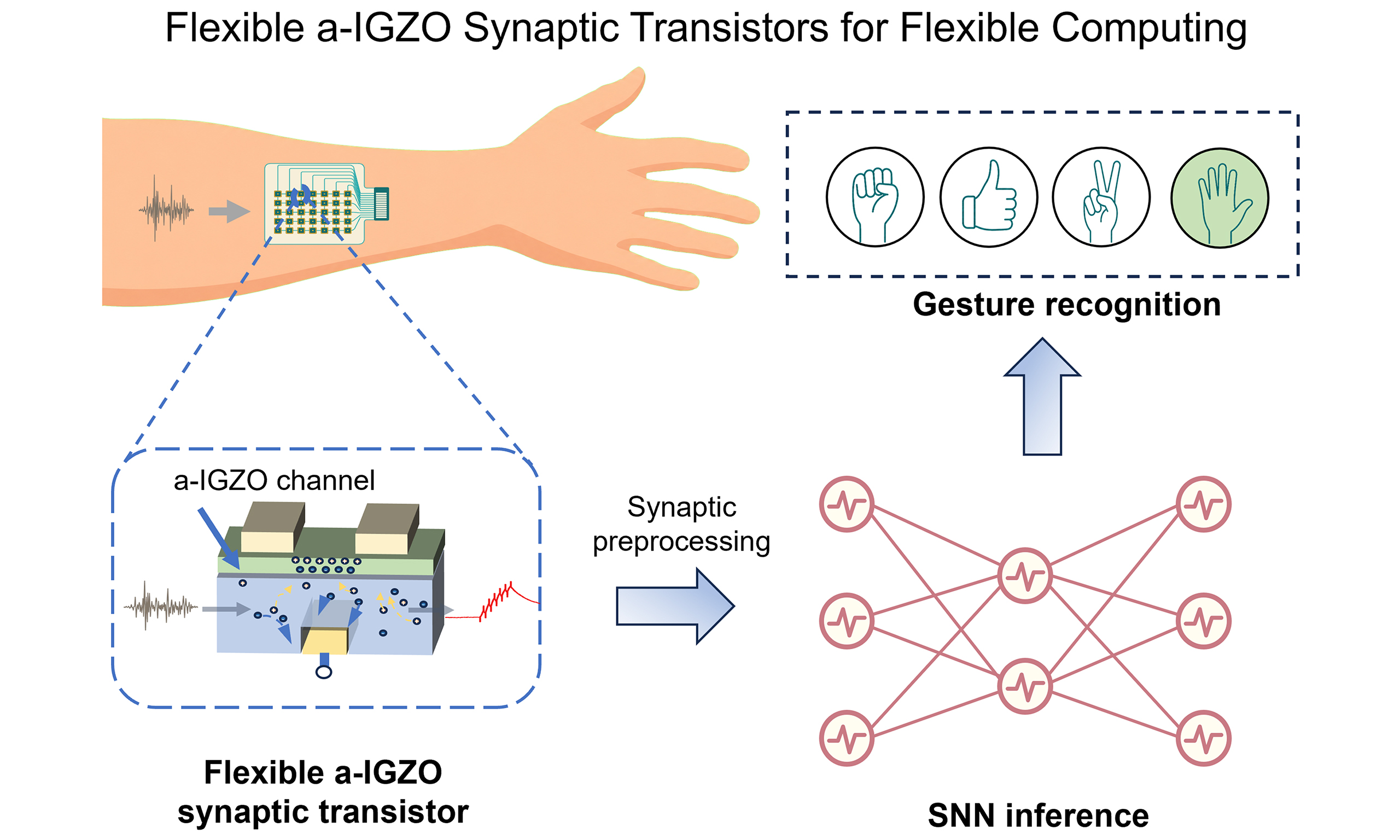
In this review, we provide an overview of flexible a-IGZO synaptic transistors from operating mechanisms to computing applications [Figure 1]. We first discuss the relationship between biological synaptic plasticity and electron transport, ionic–electronic coupling, and charge-storage mechanisms in a-IGZO devices. We then establish an evaluation framework that combines electrical performance with static and dynamic mechanical reliability. The subsequent sections examine atomic- and molecular-level materials engineering and device architecture optimization, including channel and back-channel engineering, functional dielectrics, heterointerfaces, one-dimensional (1D) channels, vertical integration, and multigate structures. Furthermore, the review discusses representative applications of a-IGZO synaptic transistors in in-sensor, near-sensor, reservoir, and in-memory computing (CIM). Finally, this review critically examines the key challenges currently hindering large-scale industrialization and outlines an evolutionary roadmap toward next-generation skin-like intelligent systems with high integration density, mechanical adaptability, and ultralow energy consumption. Overall, this review aims to provide fundamental design guidelines for the development of flexible neuromorphic hardware systems capable of simultaneously achieving high mechanical robustness, sensing-computing integration, and energy-efficient edge intelligence.
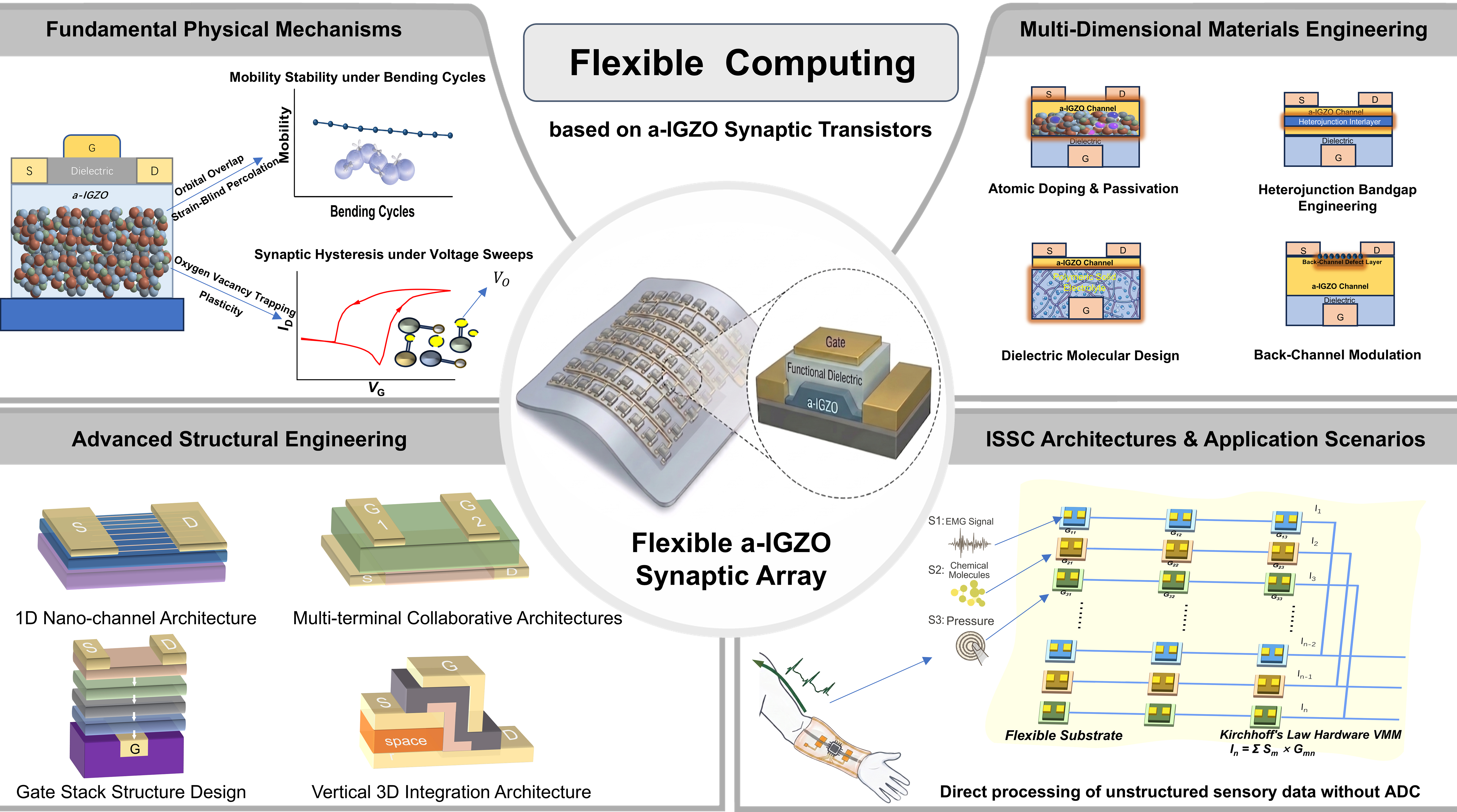
Figure 1. An overview of flexible a-IGZO synaptic transistors, illustrating the progression from fundamental physics and materials/structural engineering to macroscopic integrated sensing-storage-computing applications. a-IGZO: Amorphous indium gallium zinc oxide; ADC: analog-to-digital conversion.
OPERATING MECHANISMS AND PERFORMANCE EVALUATION OF FLEXIBLE SYNAPTIC TRANSISTORS
Flexible neuromorphic applications require synaptic transistors to reproduce relevant forms of plasticity while maintaining stable electrical and mechanical performance. This section describes the mechanisms by which a-IGZO transistors emulate synaptic responses and introduces the principal metrics used to evaluate their operation under flexible conditions.
Working mechanisms of flexible synaptic transistors
The ability of biological neural networks to process temporal information arises in part from activity-dependent changes in synaptic efficacy. As shown in Figure 2, synaptic transmission involves neurotransmitter release, receptor activation, and ion-channel gating[24]. Depending on the strength, timing, and repetition of neural activity, synapses can exhibit transient responses, referred to as short-term plasticity (STP), or longer-lasting changes associated with long-term plasticity (LTP)[25,26]. These forms of plasticity contribute to temporal filtering, learning, and memory. Artificial synaptic devices do not reproduce the underlying biological chemistry directly; instead, they map electrical or optical input pulses onto conductance changes with comparable temporal characteristics.
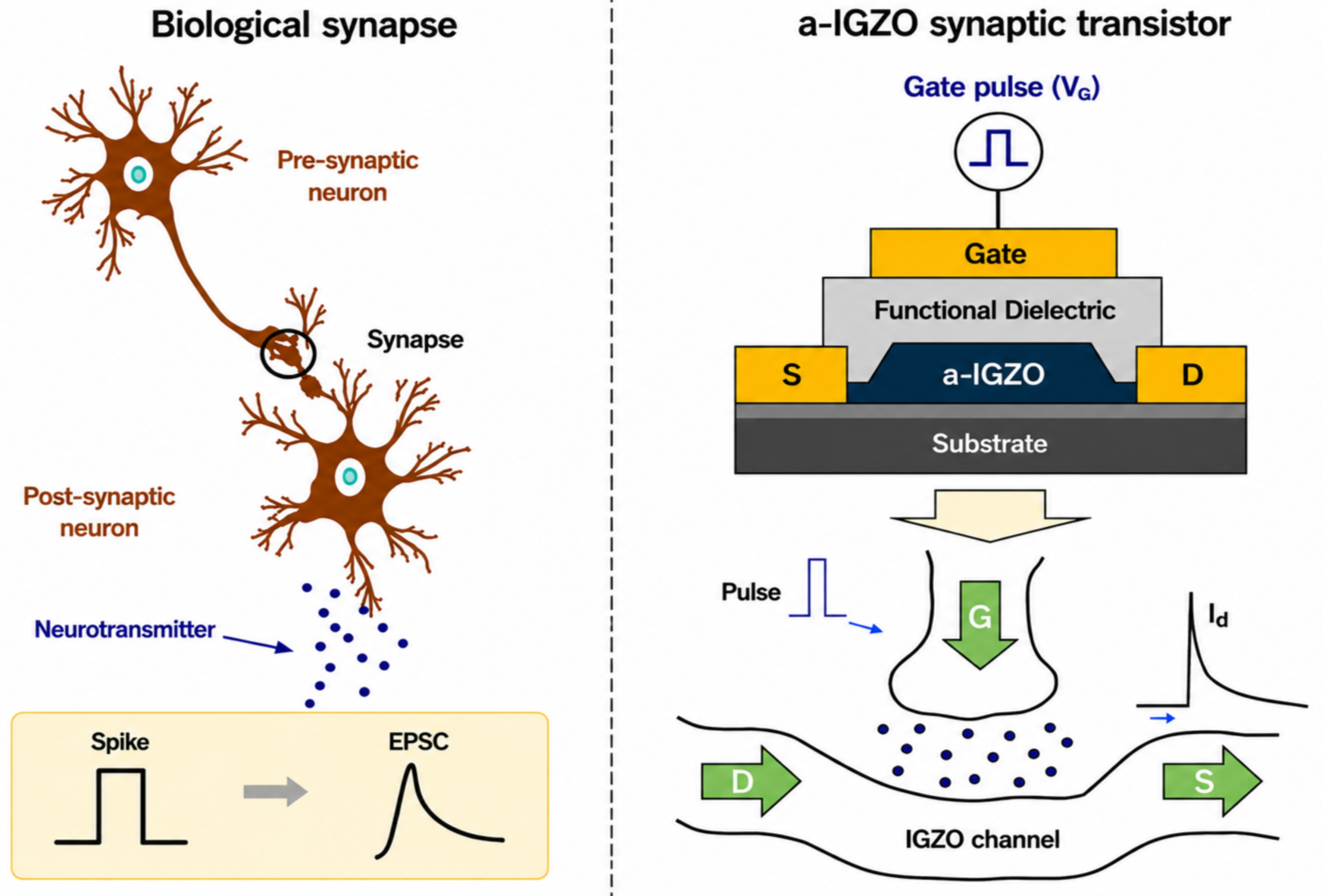
Figure 2. Biological-to-artificial synaptic mapping. Schematic illustration showing the structural and functional analogy between a biological synapse and a flexible artificial synaptic transistor, mapping neurotransmitter dynamics to channel conductance modulation. Adapted from Ref.[24] under the CC BY 3.0 license. Copyright 2015, The Authors. EPSC: Excitatory postsynaptic current; a-IGZO: amorphous indium gallium zinc oxide.
Among the candidate device structures, three-terminal a-IGZO TFTs provide a convenient platform for this functional mapping. The gate applies the presynaptic stimulus, the channel current represents the postsynaptic response, and the gate dielectric or electrolyte mediates conductance modulation. The suitability of a-IGZO as the channel material is associated with its disorder-tolerant electronic transport. The CBM of a-IGZO is mainly formed by the overlap of spatially extended and nearly isotropic 5s orbitals of heavy-metal cations, particularly In3+[15]. Unlike the strongly directional sp3 orbitals of covalently bonded semiconductors such as Si and GaAs, these orbitals are less sensitive to variations in bond angles. Effective wavefunction overlap and electronic percolation can therefore be maintained despite the absence of long-range atomic order[11,17,18].
This disorder-tolerant transport mechanism enables electron mobility above 10 cm2/Vs in optimized a-IGZO films and avoids the grain-boundary-related transport variations found in polycrystalline semiconductors. This mobility is typically one to two orders of magnitude higher than that of hydrogenated amorphous silicon (a-Si:H). Stable electrical operation has also been reported during bending in appropriately designed flexible metal-oxide TFTs[9]. For example, a-IGZO TFTs using IZO/Ag/IZO source/drain electrodes exhibited only a 5.37% reduction in field-effect mobility and a threshold-voltage shift from 0.21 to 0.72 V after 10,000 bending cycles at a radius of 10 mm[11]. However, isotropic orbital transport does not itself prevent mechanical cracking. The bending reliability of a complete device also depends on the thickness and position of the active layer, the mechanical properties of the dielectric and electrodes, interfacial adhesion, and strain distribution.
To emulate STP, many a-IGZO synaptic transistors use electric-double-layer (EDL) coupling at the electrolyte/channel interface. A gate pulse drives mobile ions, such as H+ or Li+, toward the interface, where they induce a high density of image charges in the channel. Their subsequent back-diffusion produces a transient conductance response and time-dependent relaxation[27]. The large interfacial capacitance allows substantial channel modulation at relatively low gate voltages, while the relaxation time depends on ion mobility, electrolyte composition, and pulse conditions. Longer-lasting conductance states require less volatile storage processes. Charges can be retained in deep traps within the dielectric or at the interface, in oxygen-vacancy-related states, or in an embedded floating gate, thereby shifting the threshold voltage and preserving the programmed conductance[28]. The resulting retention depends on trap depth, interfacial barriers, and the kinetics of charge release.
Ion migration and charge storage provide electrically driven plasticity but do not directly couple optical sensing to synaptic-weight modulation. This motivates optoelectronic a-IGZO devices, in which photoexcitation and persistent photoconductivity (PPC) allow light to act as both a sensory input and a programming stimulus. Illumination generates carriers and changes the occupancy of oxygen-vacancy-related states; carrier trapping or slow recombination can then sustain an elevated channel conductance after illumination[29,30]. Thus, optoelectronic a-IGZO transistors can couple optical sensing with conductance modulation, although the magnitude and persistence of the response depend strongly on defect states, illumination conditions, and device structure.
Performance evaluation of flexible synaptic transistors
Constructing flexible neuromorphic systems capable of conformally interfacing with biological tissues while performing edge computing requires a balance between the physical limitations of devices and the functional requirements of bio-inspired computing. In practical applications, such as electronic skins attached to joints, devices often operate under mechanical deformation. Flexible synaptic transistors must therefore combine mechanical deformability with reliable electrical computation, as neither property alone is sufficient for functional computing systems. Accordingly, mechanical compliance and electrical consistency should be evaluated together. Existing evaluation frameworks do not fully capture the coupled electrical and mechanical characteristics of flexible synaptic transistors[5]. This section therefore establishes a multidimensional evaluation framework covering algorithmic fidelity, energy efficiency and stability, and mechanical robustness. It evaluates both the computational accuracy of these devices as artificial synapses and their operational reliability as flexible electronic components under complex mechanical stresses.
(I) Linearity and symmetry are important metrics for assessing synaptic devices used in on-chip training. In the resistive processing unit (RPU) model proposed by Gokmen and Vlasov, an ideal weight update requires the conductance increment (ΔG) produced by each programming pulse to remain independent of the current conductance state[31]. In a-IGZO devices, nonlinear and asymmetric conductance updates can arise from nonuniform barriers during charge trapping and detrapping or from the accumulation of mobile ions at the interface. These deviations introduce weight-update errors and may reduce network convergence and training accuracy[32]. D2D variability introduces additional errors in large arrays, making fabrication uniformity as important as the intrinsic update characteristics. In an all-photolithographic array reported by our group, controlled device geometry and a homogeneous composite-electrolyte response narrowed the device distribution and reduced accumulated weight-update errors. Device-based simulations achieved a handwriting-recognition accuracy of 92.8%, with an interdevice standard deviation of 9.69%[22]. Because the effect of nonlinearity also depends on the programming scheme and network model, these device metrics should be reported together with the pulse conditions and evaluation method.
(II) Dynamic range (Gmax/Gmin) and conductance-state resolution are complementary metrics that determine how precisely synaptic weights can be represented. Although biological synapses exhibit analog changes in efficacy, hardware neural networks require a sufficient number of distinguishable and reproducible conductance states. More than 100 states correspond to a resolution exceeding 6 bits, although the required resolution depends on the network architecture and training method. The number of nominal states alone is insufficient; state-to-state variation and read noise determine whether adjacent conductance levels remain distinguishable. In flexible devices, polymer dielectrics and low-temperature-processed gate stacks may provide insufficient gate capacitance or increased leakage, thereby restricting the accessible dynamic range. Channel and gate-geometry engineering, including superlattice channels and coplanar gates, has been used to broaden the operating range without exceeding the thermal budget of flexible substrates[33,34].
(III) Efficiency and stability should be evaluated together because low-voltage operation does not necessarily ensure long-term conductance stability. For comparison, the energy associated with a biological synaptic event is commonly estimated to be approximately 1-10 fJ[35]. In electrolyte-gated transistors (EGTs), EDL capacitances above 1 μF·cm-2 can support operating voltages below 0.5 V. Attojoule-level energy consumption per event has been reported in synaptic transistors incorporating electrospun nanofiber interfaces[22,36]. However, spontaneous ion diffusion can limit the retention of the programmed state. Composite electrolytes and three-dimensional interfaces have therefore been explored to regulate ion-migration pathways and barriers, providing a means to balance programming energy against retention time[37,38]. Reported energy values should specify the pulse amplitude, pulse width, current-integration method, and device area, while retention should be measured under defined bias and environmental conditions.
(IV) Critical bending radius (Rc) is a common static measure of mechanical flexibility. Unlike rigid devices, flexible a-IGZO transistors are exposed to tensile and compressive strains during operation. According to neutral-plane mechanics, excessive strain in brittle inorganic layers can initiate microcracks, particularly when these layers are positioned away from the neutral mechanical plane[39]. Interfacial delamination may introduce an additional failure pathway. Compliant organic electrolytes, including polyvinyl alcohol (PVA)/lignin composites, can reduce elastic-modulus mismatch and suppress crack propagation, thereby improving tolerance to bending or folding[38]. Nevertheless, Rc should be reported together with device thickness, bending direction, applied strain, and the electrical state during testing because bending radius alone does not fully describe mechanical reliability.
(V) Fatigue life evaluates reliability under repeated bending or stretching and is more relevant to long-term wearable operation than a single static bending test. During more than 104 loading cycles, accumulated structural defects may increase contact resistance or eventually produce open circuits. Viscoelastic substrates and compliant device layers can dissipate strain energy and delay damage accumulation[40]. A small initial Rc therefore does not necessarily indicate high resistance to cyclic fatigue. Electrical characteristics and synaptic responses should be measured both during and after cyclic loading.
(VI) Electromechanical stability under dynamic deformation describes whether synaptic operation remains reproducible during deformation. Ideally, key characteristics - including spike-timing-dependent plasticity (STDP) time windows, pulse-response amplitudes, conductance-update trajectories, and retention - should remain within defined tolerances under different strain states. In practice, mechanical deformation can perturb ion transport, interfacial contact, and charge modulation, causing identical electrical stimuli to produce different synaptic responses, as observed in stretchable synaptic transistors[40]. Such strain-induced variations may reduce the inference accuracy of a network trained under undeformed conditions. Consequently, changes in synaptic parameters should be quantified as a function of strain and loading cycles rather than inferred only from electrical measurements performed before and after bending.
Together, these metrics highlight the need to balance electrical performance with mechanical reliability in flexible a-IGZO synaptic transistors. These trade-offs must also be considered alongside the fabrication challenges associated with a-IGZO TFT technologies[41]. A representative flexible a-IGZO synaptic transistor has demonstrated femtojoule-level energy consumption and a widely tunable memory time[42]. Nevertheless, device linearity, retention, and response consistency remain strongly dependent on the dielectric, interfaces, and deformation conditions. The following sections discuss material- and device-architecture strategies for improving these properties while preserving mechanical durability.
STRATEGIES FOR ENHANCING THE PERFORMANCE OF FLEXIBLE SYNAPTIC TRANSISTORS
Two main routes are used to prepare a-IGZO thin films: vacuum-based deposition, including sputtering, pulsed-laser deposition (PLD), and atomic layer deposition (ALD), and solution-based processing, including spin coating and printing. Representative results from these techniques are compared in Table 1. Vacuum deposition generally provides dense films and precise control over film thickness and composition, whereas solution processing reduces equipment requirements and is compatible with printing and patterned deposition. However, solution-derived a-IGZO films often require thermal, photochemical, or combustion treatments to remove organic residues and form dense metal–oxygen networks. Selection of the deposition method therefore involves trade-offs among film quality, thermal budget, manufacturing cost, and scalability.
Comparison of representative dry and solution-based techniques for the deposition of a-IGZO thin films
| Processing category | Technique | Representative temperature (°C) | Reported mobility (μ, cm2/Vs) | Reported characteristics | Ref. |
| Dry deposition | PLD | Room temperature | ~8.3 | Flexible-substrate compatible | [15] |
| Thermal ALD | 200; no post-annealing | ~23.6-25.6 | Conformal; compositionally uniform | [43] | |
| Solution processing | Spin-coating (solution combustion) | 300 | ~3.2 | Fully solution-processed; reproducible | [44] |
| Inkjet printing | 300 | 20.6 ± 4.3 | Dense films; consistent line width | [45] |
For flexible a-IGZO devices, the selection of deposition and post-treatment methods is further constrained by the thermal stability of polymer substrates, which generally limits process temperatures to below 300 °C. Low-temperature deposition and annealing can leave a relatively high concentration of oxygen vacancies (Vo) and subgap states in a-IGZO films[46]. Because the formation of continuous metal–oxygen networks generally requires thermal activation, this constraint complicates the simultaneous optimization of film density, carrier transport, and substrate compatibility.
These defect states can serve as charge-trapping centers that support synaptic plasticity[18,47], but they can also compromise device stability. Changes in the charge state of metastable Vo under prolonged electrical bias or illumination may cause programmed conductance states to relax over time[47]. Trap depth introduces a further trade-off: deep traps can improve retention but usually require higher programming energy, whereas shallow traps enable faster responses but provide less persistent conductance modulation[48,49]. In scaled devices, stochastic trapping and detrapping at a limited number of interfacial sites can also produce random telegraph noise (RTN), degrading weight-update linearity and array uniformity[50].
Because these limitations cannot always be addressed by optimizing deposition conditions alone, material- and device-engineering approaches for flexible a-IGZO synaptic transistors are examined in detail in the following sections. Section “Materials engineering” discusses materials engineering at the channel, back channel, gate dielectric, and heterointerfaces, whereas Section “Structural reconfiguration” addresses device-architecture engineering.
Materials engineering
Channel-material selection establishes the fundamental trade-offs between electrical performance and mechanical compliance in flexible neuromorphic devices. Representative conjugated polymers and a-IGZO occupy complementary positions in this respect. As summarized in Table 2, a-IGZO generally provides higher carrier mobility and better electrical stability, whereas conjugated polymers offer greater intrinsic softness and tolerance to tensile strain.
Comparison of a-IGZO and conjugated polymers for flexible neuromorphic hardware
| Feature | a-IGZO[9,15] | Conjugated polymers (e.g., PEDOT:PSS, P3HT)[14,51] |
| Transport mechanism | Isotropic s-orbital overlap (electron-dominated) | Ion-electron coupling/hopping mechanism |
| Typical mobility (μ) | High (typically > 10 cm2/Vs) | Relatively low (typically < 1 cm2/Vs) |
| Operating timescale | Tunable and fast (nanoseconds to milliseconds) | Inherently slow (milliseconds to seconds), naturally matches biology |
| Mechanical property | Bendable, but vulnerable to cracking under high tensile strain | Intrinsically soft and stretchable (can withstand high tensile strain) |
For a-IGZO, materials engineering is therefore central to preserving its favorable carrier transport and electrical stability while improving energy efficiency, functional response, and compatibility with the processing and operating requirements of flexible neuromorphic devices. Because a single compositional adjustment rarely provides high mobility, reliable conductance modulation, and multimodal sensing simultaneously, recent studies have combined several forms of material control. Rather than relying only on deposition optimization, these approaches target the electronic structure, ionic dynamics, and interfacial energy landscape that govern carrier generation, transport, and storage. They include modifying channel composition and defects, functionalizing the back channel, regulating ion motion or ferroelectric polarization in the gate dielectric, and introducing heterointerfaces to modify optical absorption and carrier separation. The following subsections examine these strategies together with the processing and stability constraints relevant to flexible devices.
Regulation of channel atomic components
In amorphous oxide semiconductors (AOSs), metastable oxygen-related defects, particularly Vo, play a major role in threshold-voltage shifts (ΔVth) under bias stress and can also contribute to nonlinear conductance updates in synaptic devices. In the archetypal ternary In-Ga-Zn-O system, the electronic properties of the film are governed by the orbital characteristics and metal–oxygen bonding of its constituent cations. The spatially extended, nearly isotropic In 5s orbitals provide the principal electron-transport pathways, whereas the stronger affinity of Ga for oxygen suppresses excessive carrier generation and oxygen-vacancy formation; Zn contributes to the formation of the amorphous oxide network[17,18,52]. The stabilizing effect of Ga is commonly associated with the higher reported bond dissociation energy of Ga-O (~374 kJ/mol) relative to In-O (~346 kJ/mol)[52]. Consequently, the comparatively weaker In-O bonding may make In-rich compositions more susceptible to oxygen loss and defect formation during energetic processing or prolonged electrical or optical stress. Increasing the Ga content can improve stability, but the smaller spatial extent of Ga 4s orbitals may impede carrier transport. This composition-property relationship also explains why nominal stoichiometry cannot be evaluated independently of deposition and post-treatment conditions. Channel composition must therefore balance carrier mobility against defect-related stability.
One approach to this trade-off is to introduce an additional metal cation that modifies the electronic states near the CBM. The heavy-metal-cation orbital-overlap model proposed by Hosono identifies the overlap of spatially extended ns orbitals as an important factor governing electron transport in amorphous oxides[15]. On this basis, Sn can replace Ga to form indium–tin–zinc oxide (ITZO) or partially substitute for Ga to form indium–gallium–zinc–tin oxide (IGZTO)[53]. Because Sn and In are both fifth-period cations with spatially extended 5s orbitals, Sn provides a transport contribution more similar to that of In than to the smaller Ga 4s orbital. Overlap between the Sn and In 5s states can form broader and more continuous electronic percolation pathways near the CBM. This modification can reduce the electron effective mass and increase field-effect mobility while retaining some suppression of oxygen-vacancy formation[54]. The wider percolation network may also support rapid modulation of channel conductance during synaptic operation. However, the resulting carrier concentration and subthreshold characteristics remain sensitive to composition, oxygen partial pressure, and other deposition conditions[53,54].
When bias stability is prioritized, Hf-based channel engineering provides a complementary strategy for regulating oxygen-related defects. An Hf-doped a-IGZO back-channel layer can act as an oxygen scavenger and redistribute oxygen near the channel interface, while Hf-doped IGZO layers can suppress Vo and other oxygen-related defects, thereby improving bias stability[55,56]. However, the effects of Hf remain concentration-dependent, because excessive suppression of oxygen-related donors can reduce carrier density and alter mobility. Location-selective chloride modulation doping provides another means of controlling defect states, as demonstrated in the dual-channel device shown in Figure 3A(i)[57]. The ion-regulated band model in Figure 3A(ii) illustrates how chloride incorporation modulates the electronic structure of the doped channel. Chloride incorporation suppresses persistent photocarrier excitation and reduces the density of oxygen-vacancy-related subgap states, consistent with the O 1s X-ray photoelectron spectroscopy results shown in Figure 3A(iii). The electrical measurements further indicate reduced threshold-voltage drift in the doped channel[57]. Unlike uniform channel doping, this spatially selective approach can improve stability without modifying the entire transport channel.
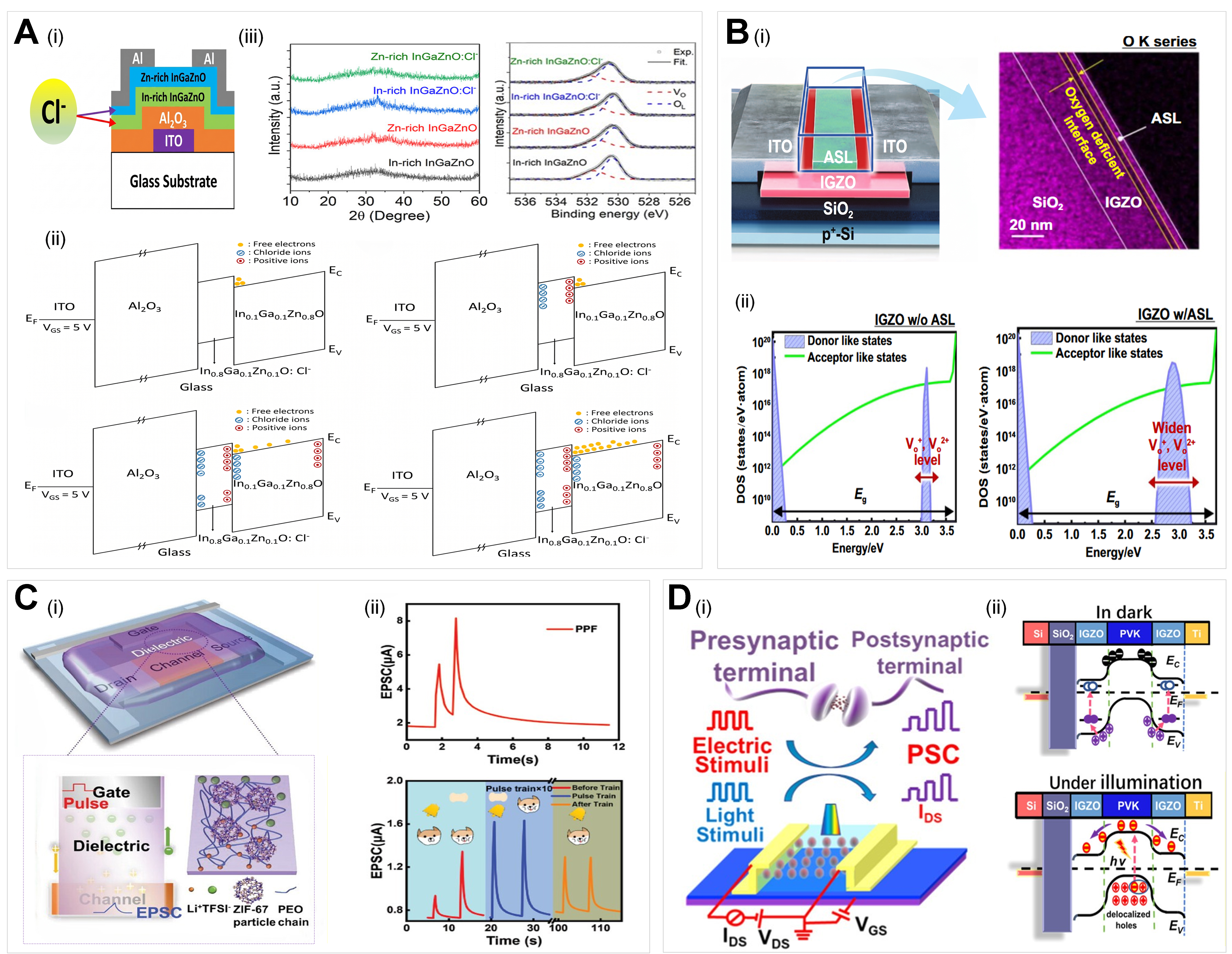
Figure 3. Materials engineering and microscopic mechanism regulation of a-IGZO synaptic transistors. (A) Channel atomic components: (i) Schematic illustration of the location-selective chloride (Cl-) modulation-doped IGZO dual-channel synaptic transistors. (ii) Energy band and ion distribution model during the potentiation process, elucidating the ion-regulated synaptic weight update mechanism. (iii) O 1s XPS spectra and XRD patterns of the channel regions, demonstrating the passivation and modulation of Vo levels via Cl-doping. Adapted from Ref.[57] under the CC BY 4.0 license. Copyright 2025, The Authors; (B) Back-channel engineering: (i) 3D schematic illustration of an IGZO phototransistor featuring an ASL at the back-channel, alongside the cross-sectional image and EDS mapping highlighting the oxygen-deficient interface. (ii) Proposed subgap DOS models for the IGZO phototransistors without and with the ASL, illustrating the widened subgap defect levels. Adapted from Ref.[62] under the CC BY 4.0 license. Copyright 2025, The Authors; (C) Molecular dynamics of dielectric: (i) Schematic of an individual EGT in a high-density artificial synapse array (100 × 100) with a lateral-gate structure, highlighting the ionic conduction framework enhanced by ZIF-67 porosity. (ii) Representative PPF and long-term EPSC responses, showing the enhanced synaptic performance. Adapted from Ref.[22] under the CC BY 4.0 license. Copyright 2023, The Authors; (D) Heterojunction bandgap engineering: (i) Schematic of emulating a biological synapse using an IGZO/CsPbBr3 NPs/IGZO TFT architecture under electrical and optical stimuli. (ii) Schematic energy-band diagrams of the IGZO/CsPbBr3 NPs/IGZO heterostructure in the dark and under illumination, illustrating photocarrier separation and transfer. Adapted with permission[76]. Copyright 2021, American Chemical Society. a-IGZO: Amorphous indium gallium zinc oxide; XPS: X-ray photoelectron spectroscopy; XRD: X-ray diffraction; ASL: aluminum sensitization layer; EDS: energy-dispersive X-ray spectroscopy; DOS: density of states; EGT: electrolyte-gated transistor; PPF: paired-pulse facilitation; EPSC: excitatory postsynaptic current; NPs: nanoparticles; TFT: thin-film transistor; ITO: indium tin oxide; PEO: poly(ethylene oxide); PVK: perovskite.
Post-treatment provides an additional route for passivating dangling bonds and nanovoids produced during low-temperature film formation. Hydrogen annealing can passivate some defects, although excessive hydrogen may introduce donor states, increase channel conductivity, and degrade switching behavior. Nitrogen-plasma treatment has also been used to passivate oxygen-vacancy-related sites through the formation of metal–nitrogen bonds. In an IGZO-based resistive memory device, this treatment improved resistive-switching stability and carrier injection at the contact region[58]. This result supports the underlying passivation mechanism, although the reported device is not a three-terminal synaptic transistor.
Supercritical-fluid (SCF) treatment provides a low-temperature method for transporting reactive molecules into dense oxide films. Unlike conventional gas-phase annealing, which may be limited by diffusion into dense films, a supercritical medium combines gas-like diffusivity with liquid-like solvent capacity. Chen et al. used supercritical CO2 at temperatures above 31 °C and pressures above 7.38 MPa to deliver polar H2O or NH3 molecules into the film[20]. These properties facilitate oxidation and hydrogen-bond-network reconstruction, reducing deep subgap defects and improving synaptic-weight linearity. Density functional theory (DFT) calculations further indicate that moderate nitrogen incorporation and the resulting metal–nitrogen bonds can modify the valence-band maximum (VBM), suppress unwanted hole-related processes, and improve light stability and current modulation[59]. For large-area flexible devices, the uniformity of molecular delivery and passivation across the channel remains an important processing consideration. Overall, compositional doping and low-temperature passivation provide complementary means of balancing mobility and defect stability, but their effectiveness depends strongly on dopant concentration, spatial distribution, and process control; spatially selective treatments may therefore be particularly suitable for flexible devices with restricted thermal budgets.
Back-channel defect engineering
In traditional bottom-gate staggered a-IGZO TFTs, the physical surface of the exposed channel (i.e., back-channel) often causes reliability degradation due to the adsorption of environmental moisture and oxygen. However, from the perspective of neuromorphic engineering, this highly open interface precisely provides an ideal physical “anchor” for cross-scale material compounding. By introducing localized metal sensitization structures or customized deep-level defect layers at the back-channel, the “high-mobility transport” and “non-volatile storage” paths of carriers can be effectively decoupled.
Because the wide bandgap of a-IGZO limits its intrinsic absorption of visible light, metal nanostructures have been introduced at the back channel to enhance the photoresponse. Kim et al. proposed the controlled deposition of core-shell structured aluminum nanoparticles (Al NPs, ~6 nm)[60]. Utilizing the localized surface plasmon resonance (LSPR) effect of the Al0 core, hot electrons are efficiently pumped across the native Al2O3 oxide shell into the IGZO conduction band, achieving synaptic weight modulation with extremely low energy consumption[60,61]. Furthermore, the metallic sensitization island [aluminum sensitization layer (ASL)] structure [Figure 3B(i)] developed by Kwak et al. not only physically suppresses dark current but also induces a widened subgap density of states (DOS) at the back-channel interface [Figure 3B(ii)]. This engineering strategy endows the device with a high signal-to-noise ratio and strong transient response capability, while enabling over 256 conductance states and 128-level LTP/LTD characteristics, successfully demonstrating the wide dynamic-range adaptation characteristics of the biological retina[62].
Back-channel traps can also move the charge-storage region away from the gate-dielectric/channel interface. In conventional dielectric-trapping synaptic transistors, stored interfacial charge may increase Coulomb scattering and reduce carrier mobility. Yang et al. therefore introduced titanium-oxide-related traps at the back channel of a dual-gate InGaZnO synaptic transistor[63]. In this configuration, the high-k gate dielectric provides capacitive coupling, whereas trapping and detrapping at TiOx-associated defects regulate longer-term conductance states. This functional separation limits the influence of dielectric-trap-related scattering on the principal transport pathway. The device retained a carrier mobility of approximately 11.5 cm2/Vs, with a D2D variation of approximately 7.2% in conductance modulation[63]. The reported image-classification performance was obtained from a convolutional neural network simulation based on measured device characteristics rather than from a fully integrated hardware system.
Back-channel engineering can therefore enhance optical sensitivity or provide charge-storage sites while preserving channel transport. However, device performance remains sensitive to environmental adsorption, sensitizer coverage, trap distribution, and interface stability. Because the operating voltage and temporal response are also governed by gate coupling, further optimization requires suitable gate-dielectric materials, as discussed in the following subsection.
Gate-dielectric engineering
In synaptic TFTs, the gate dielectric determines the capacitive coupling, operating voltage, and temporal response of conductance modulation. Conventional SiO2 and SiNx dielectrics have relatively limited areal capacitance unless they are made very thin, which can restrict low-voltage operation. Dielectric engineering has therefore focused mainly on ionically conducting electrolytes, which form EDLs, and ferroelectric materials, which provide polarization-dependent memory. These two dielectric classes offer different temporal characteristics and impose different requirements on processing and device stability.
As discussed in Section “Working mechanisms of flexible synaptic transistors”, EDL formation at an electrolyte/channel interface produces a large interfacial capacitance and enables substantial channel modulation at low gate voltages. Biomass-derived hydrogels have consequently been investigated as flexible proton-conducting gate dielectrics for metal-oxide synaptic transistors[64]. Representative examples include PVA/lignin composite electrolytes[38] and chitosan-based dielectrics[65,66]. In hydrated biopolymers, proton transport is commonly attributed to hopping along hydrogen-bond networks through a Grotthuss-type mechanism, and its rate therefore depends strongly on water content and the density of polar functional groups. Although these materials offer flexibility and potential biocompatibility, humidity-dependent swelling, limited thermal and chemical stability, and incompatibility with some photolithographic processes can hinder array fabrication. Process-compatible barrier layers and device structures can alleviate some of these limitations[65]. Li et al. demonstrated a 100 × 100 array of lateral-gate EGTs, integrated within an area of 2.5 × 2.5 mm2 and incorporating a porous ZIF-67 framework to facilitate ionic transport [Figure 3C(i)][22]. The array showed relatively uniform paired-pulse facilitation (PPF) and longer-term excitatory postsynaptic current (EPSC) responses, as illustrated in Figure 3C(ii), indicating that electrolyte-gated devices can be integrated at higher density under the reported fabrication conditions.
Photocrosslinkable polymer dielectrics provide a complementary route toward solution processing and patterned integration. Kwak et al. used ultraviolet (UV)-induced thiol–ene crosslinking to form a P(NB/VNB) copolymer dielectric in an all-solution-processed IGZO synaptic transistor[34]. Residual hydroxyl groups in the crosslinked dielectric produced slow dipolar polarization at the dielectric/IGZO interface, enabling a large conductance dynamic range and stable operation under repeated pulsing. Unlike proton transport in hydrated biopolymers, the synaptic response in this device arises primarily from slow interfacial dipolar polarization.
Ion gels provide another solid-state electrolyte option. They confine an ionic liquid within a polymer network and combine high ionic conductivity with low volatility and a relatively wide electrochemical window. Ionic transport and thermal response can be adjusted through the choice of ionic liquid and polymer network. Operation over -50 to 110 °C has been reported for ion-gel-gated organic electrochemical transistors[67], while specially designed ion gels have supported EGT operation at elevated temperatures[68]. Because these demonstrations used transistor platforms other than a-IGZO synaptic arrays, their transfer to flexible a-IGZO devices still requires evaluation of semiconductor/electrolyte compatibility, mechanical reliability, and long-term ion retention.
Ferroelectric HfO2-based dielectrics, including Hf0.5Zr0.5O2 (HZO), provide a different route in which remanent polarization modulates the channel conductance without relying on slow ionic relaxation. Polarization reversal shifts the threshold voltage, while partial domain switching can generate intermediate conductance states for analog weight modulation. Stabilization of the metastable orthorhombic phase depends on dopant concentration, film thickness, thermal treatment, and mechanical confinement by the electrodes[69,70]. Goh et al., for example, reported that tensile stress induced by a W bottom electrode stabilized ferroelectricity in a 4.5-nm HZO ferroelectric tunnel junction[71]. HfO2-based ferroelectrics nevertheless remain subject to wake-up, fatigue, leakage, and D2D variability, all of which can affect analog weight updates. Dielectric engineering can therefore reduce operating voltage and provide either volatile ionic dynamics or nonvolatile polarization states, but processing compatibility and long-term stability remain material-specific constraints. Extending a-IGZO devices to broader optical sensing functions consequently requires complementary heterointerface engineering, as discussed in the following subsection.
Heterojunction bandgap engineering
The optical bandgap of a-IGZO is typically approximately 3.0-3.3 eV; consequently, its intrinsic interband absorption is concentrated in the ultraviolet region, although defect-mediated subgap responses may also occur. Coupling a-IGZO to narrower-bandgap absorbers can extend its spectral response while retaining the oxide channel for charge transport. Appropriate band offsets can facilitate photocarrier separation and produce photogating or charge-retention effects. However, these benefits depend on interface quality because additional traps may also increase dark current, slow recovery, or reduce operational stability.
Mixed-dimensional heterostructures integrate materials of different dimensionalities and provide a general framework for combining their optical and electronic properties[72]. Chen et al. coupled low-toxicity CuZnInSSe (CIZS) colloidal quantum dots with a-IGZO to form a visible-light-sensitive phototransistor array[73]. Ligand exchange adjusted the photoresponse time from approximately 0.3 to 11 s, allowing the devices to operate in either a rapid-sensing mode or a longer-lived neuromorphic visual mode[73]. Zhu et al. used an IGZO/CdS-quantum-dot/polymethyl methacrylate (PMMA) heterojunction to extend the response to 655-nm illumination and demonstrated luminance-based color-to-gray conversion using spike encoding[74,75]. As a representative example of such heterogeneous interfaces, Duan et al. designed a channel layer with CsPbBr3 perovskite nanoparticles [denoted as perovskite nanoparticles (PVK NPs) in Figure 3D(i)] buried in an IGZO film to emulate biological synapses. This configuration establishes a perfect Type-II energy band alignment in the dark and under illumination [Figure 3D(ii)], ensuring that photo-generated electrons efficiently slide down to the IGZO channel while holes remain trapped. The resulting devices exhibit robust transient optoelectronic EPSC responses under varying light intensities, which provides a reliable physical foundation for spatiotemporal visual processing[76].
Two-dimensional (2D) light absorbers provide a related approach. In MoS2–IGZO heterojunction phototransistors, MoS2 absorbs visible light while a-IGZO serves as the transport channel; a responsivity of approximately 1.7 A·W-1 was reported at 520 nm under an optical power of 1 μW[77]. This result supports spectral extension through interfacial charge transfer but does not establish ballistic transport across the interface. IGZO/SnSx/IGZO heterojunction phototransistor arrays have also combined the low dark current of IGZO with visible-light absorption in SnSx for image sensing[78]. Separately, selective IGZO deposition on WSe2 has been used to form a lateral p–n junction with ultraviolet-to-near-infrared photodetection and a photovoltaic response near zero drain bias[79]. The latter two studies concern photodetection rather than synaptic plasticity and should therefore be regarded as potential interface designs for future optoelectronic synaptic devices.
Together, channel-composition control, back-channel functionalization, gate-dielectric engineering, and heterointerface design can improve stability, operating voltage, and sensory functionality in a-IGZO synaptic transistors. Their effects nevertheless remain coupled to defect density, interface quality, environmental stability, and fabrication compatibility. Material-level optimization alone also does not resolve device footprint, array layout, or electrostatic-control constraints; these issues motivate the structural reconfiguration strategies discussed in Section “Structural reconfiguration”.
Structural reconfiguration
Material engineering modifies charge transport and storage at the material and interface levels, whereas structural engineering controls gate coupling, current pathways, and integration density at the device level. Conventional planar single-gate architectures may face trade-offs among linear weight modulation, operating voltage, and cell density. Recent studies have therefore explored several complementary strategies, including gate-stack design, 1D nanochannels, vertical integration, and multi-terminal architectures. Representative architecture-engineering strategies are illustrated in Figure 4 and discussed in detail in the following subsections.

Figure 4. Structural reconfiguration of flexible a-IGZO synaptic transistors. (A) Floating-gate stack engineering: (i) Schematics of IGZO synaptic transistors incorporating IGZO and ITO floating gates, respectively. (ii) Transfer characteristics of the two devices measured under a gate double sweep from -15 to 15 V. (iii) Retention characteristics of the programmed and erased states for devices with IGZO and ITO floating gates. Adapted from Ref.[28] under the CC BY 4.0 license. Copyright 2025, The Authors; (B) 1D Nanochannel architecture: (i) 3D schematic of an IGZO/In2O3 NW heterojunction phototransistor stimulated by a UV light pulse. (ii) Transient current responses at various pulse frequencies and the corresponding extracted SRDP. Adapted with permission from[89]. Copyright 2024, Elsevier; (C) Vertical 3D integration: (i) Cross-sectional schematic and TEM image of a vertical-channel synapse TFT, minimizing device footprint via HfO2 spacer engineering. Adapted with permission[91]. Copyright 2025, American Chemical Society. (ii) Schematic of high-performance IGZO CAA transistors featuring in situ engineered vertical indium gradients. (iii) Comparison of vertical In:Ga atomic ratios at deposition pressures of 30 mTorr. Adapted with permission[92]. Copyright 2026, American Chemical Society; (D) Multi-terminal collaborative architecture: (i) Illustration of a hetero-synapse excited by electric inputs from two presynaptic terminals and the corresponding electrochemical ion modulation of the channel layer under dual-terminal gating. (ii) Postsynaptic currents (EPSCs) excited by five presynaptic spikes separately or simultaneously applied to G1 and G2 terminals. (iii) Architecture of the neural network based on the hetero-synaptic transistor for MNIST image recognition. (iv) Comparison of classification accuracy between networks based on the dual-gate hetero-synaptic transistor and the single-gate homo-synaptic transistor. Adapted with permission[105]. Copyright 2022, The Royal Society of Chemistry. a-IGZO: Amorphous indium gallium zinc oxide; ITO: indium tin oxide; NW: nanowire; UV: ultraviolet; SRDP: spike-rate-dependent plasticity; TEM: transmission electron microscopy; TFT: thin-film transistor; CAA: channel-all-around; EPSCs: excitatory postsynaptic currents; MNIST: Modified National Institute of Standards and Technology; PL: protection layer; CH: channel; TL: tunneling layer; FG: floating gate; PAD: pad (contact pad); GI: gate insulator; ACT: active layer.
Gate stack structure design
Within planar devices, gate-stack design can introduce ion migration, charge trapping, or ferroelectric polarization as additional state variables for conductance modulation. EGTs employ an electrolyte in place of a conventional gate dielectric, producing strong interfacial capacitive coupling and time-dependent ionic responses at relatively low operating voltages. Their practical integration, however, depends on the patternability and process compatibility of the electrolyte. Hou et al. developed coplanar all-solid-state electrolyte-gated IGZO artificial synapses[80]. Li et al. subsequently demonstrated an optoelectronic IGZO synaptic transistor with a solid-state electrolyte for nociceptive-response emulation, avoiding the liquid leakage associated with liquid-electrolyte EGTs[81].
Although EGTs exhibit excellent energy efficiency, the volatility of ion physical adsorption limits their data retention (usually < 104 s). To address this issue, researchers have drawn inspiration from flash technology, introducing charge trapping structures (CTS) based on deep potential wells into the a-IGZO system. Unlike traditional polycrystalline silicon floating-gate cells, the current optimization direction has shifted toward fine structure engineering. For example, Jeong et al. successfully utilized AOS-based charge trap TFTs, achieving wavelength-dependent erasing under visible light to precisely tune memory states and enhance neuromorphic display performance[82]. Furthermore, to simplify the process complexity brought by multi-layer stacking, Jang et al. proposed utilizing an embedded ZnO layer deposited under the a-IGZO as an inherent charge-trapping center, effectively prolonging memory retention for advanced reservoir computing (RC) while eliminating the complex fabrication steps of metal floating gates and greatly reducing integration costs[83].
Ferroelectric field-effect transistors (FeFETs) provide nonvolatile conductance modulation through polarization switching. In metal–ferroelectric–insulator–semiconductor structures, a high-k buffer layer can modify the electric-field distribution and reduce direct interaction between a-IGZO and the ferroelectric layer[84]. Kwon et al. further showed that an Al2O3/HfO2 dielectric stack can support sweep-rate-dependent competition between ferroelectric polarization and trap-assisted switching, enabling the electrical modulation of synaptic plasticity and conductance-update linearity[85].
Floating-gate engineering provides another route for introducing nonvolatile state variables into the gate stack. Park et al. compared IGZO synaptic transistors incorporating IGZO and indium tin oxide (ITO) floating gates[28]. As illustrated in Figure 4A(i), the floating gate was incorporated between the gate dielectric and the Al2O3 tunneling layer, allowing the threshold voltage to be programmed through charge transfer between the channel and the floating gate. Both devices exhibited clockwise hysteresis during gate double sweeps [Figure 4A(ii)]; however, the smoother ITO/Al2O3 interface reduced defect-assisted charge loss and improved the retention of the programmed states compared with the IGZO floating gate [Figure 4A(iii)]. The ITO-floating-gate devices were further implemented in a 64-device synaptic array, demonstrating that material selection within the gate stack affects not only single-device memory characteristics but also array-level weight uniformity. Although the devices were demonstrated on a rigid substrate, the results provide a relevant gate-stack design strategy for future flexible integration, provided that the thermal budget and mechanical compatibility of the dielectric and floating-gate layers are addressed.
Lee et al. further demonstrated an HZO-based transistor in which optical and electrical stimuli modulated the conductance through the gate stack[86]. Gate-stack engineering can therefore provide low-voltage ionic dynamics, charge-trap or floating-gate memory, and ferroelectric polarization states, although retention, update linearity, fabrication complexity, and mechanical compatibility remain dependent on the selected stack.
1D nanochannel design
As device feature sizes approach the limits of short-channel effects (SCE), enhancing the electrostatic control capability of the gate by reducing the channel dimensionality has become an inevitable trend. 1D nanofiber or nanowire structures, due to their extremely high surface-to-volume ratio and unique electronic confinement effects, exhibit enhanced potential over continuous thin films in terms of energy efficiency, sensing sensitivity, and mechanical flexibility.
Electrospinning is widely used as a low-cost, scalable bottom-up manufacturing technology for constructing quasi-1D oxide semiconductor networks. A typical fabrication process involves preparing hybrid precursor solutions containing IGZO precursors and organic components, followed by precise rheological control, ultimately forming a nonwoven nanofiber network with tunable structural parameters.
Subsequent thermal annealing (calcination) is a key step determining the microscopic structure and electrical performance of the fibers. Adopting an optimized multi-stage heating program is crucial to gently decompose the organic template, such as polyvinylpyrrolidone (PVP), while avoiding undesired crystallization, thereby preserving the amorphous nature of IGZO. Rapid heating causes rapid gas evolution from organic components, forming nanopores or even fractures on the fiber surface, which can impede carrier-transport pathways. After optimizing the calcination process, a dense and robust amorphous M-O-M continuous network is formed. Jiang et al. conducted systematic explorations in this field, demonstrating electrospinning-driven IGZO nanofiber phototransistors that successfully bridge adaptive processing and recognition learning[87]. Fu et al. successfully utilized this strategy to fabricate IGZO/PVP composite nanofiber neuromorphic transistors with excellent optoelectronic synapse emulation and RC capabilities[88]. From a physical-mechanism perspective, this quasi-1D network structure possesses multiple intrinsic advantages. On the one hand, the physical cross-junctions between intersecting nanofibers constitute a natural percolation barrier network. As demonstrated in heterojunction architectures like IGZO/In2O3 NW/IGZO [Figure 4B(i)], this junction-dominated transport mode is highly sensitive to external stimulation. Under UV-light stimulation, the device exhibits multilevel conductance modulation and highly tunable spike-rate-dependent plasticity (SRDP), as shown in Figure 4B(ii), ultimately achieving an image-recognition accuracy of 95.3%[89].
On the other hand, the 3D-like nature of the nanowire/nanofiber channels allows for enhanced gate field modulation. Related studies of electrospun SnO2 nanofiber transistors have also shown that a three-dimensional network interface can support low-energy paired-pulse-facilitation responses[37]. Because these results were obtained using a different oxide semiconductor, they provide comparative evidence for the influence of channel geometry rather than direct evidence for a-IGZO devices.
To further address the uniformity and scalability issues inherent to disordered nanofiber networks, researchers have proposed advanced alignment architectures. Utilizing highly integrated IGZO/InHfOx nanowire architectures, Luo et al. demonstrated high-accuracy temporal visual information processing. Aligned nanowire architectures and their coupling to external processing hardware may improve the reproducibility of temporal signal processing[90]. Nevertheless, diameter variation, fiber alignment, interwire junctions, and thermal treatment remain important constraints on large-area nanochannel arrays.
Vertical three-dimensional integration design
To break the geometric limits placed on device density by photolithography resolution in planar 2D arrays, the vertical-channel transistor (Vertical-TFT, V-TFT) architecture, with the channel oriented vertically, has emerged. The core of this revolution lies in the dimensional transformation of the design concept - the channel length (L) is no longer defined by the horizontal precision of the photolithography machine, but by the vertical thickness of the deposited thin film. In a typical vertical structure, source and drain electrodes are separated vertically by an insulating spacer. This geometry enables significant minimization of the device footprint and energy consumption. For instance, Jang et al. successfully demonstrated vertical synapse thin film transistors (VS-TFTs) with an ultra-short channel length (Lch) of 40 nm utilizing an ALD-deposited InGaZnO active layer and precise spacer engineering of HfO2 [Figure 4C(i)], which effectively ensures conformal coverage and ultralow power consumption[91]. Furthermore, to push the density limits of monolithic 3D integration beyond spacer-defined structures, the channel-all-around (CAA) architecture has emerged as a promising solution [Figure 4C(ii)]. Instead of conventional uniform doping, Sun et al. proposed the in situ engineering of vertical indium (In) gradients via sputtering kinetics. This sophisticated gradient design optimizes the carrier distribution within the vertical channel [Figure 4C(iii)], significantly suppressing off-state leakage while boosting effective mobility. Such CAA-based architectures not only provide superior electrostatic control but also enable high-performance neuromorphic computing within an ultra-compact vertical footprint[92]. Additionally, integrating vertically aligned nanocomposites with highly defective channels can further enhance the robustness and density of neuromorphic devices[93].
However, this vertical topology poses severe challenges to fabrication processes, primarily in ensuring continuous conformal coverage and suppressing parasitic effects caused by the vertical overlap of electrodes. To address these issues, parasitic conduction paths and capacitance must be strictly controlled to enhance the device’s high-frequency response. Researchers have developed advanced methodologies, such as electrohydrodynamic jet-printing, to effectively tune the subthreshold swing and modulate these parasitic conduction paths[94], while simultaneously utilizing the aforementioned HfO2 spacer engineering to optimize the physical separation and electric field distribution within the vertical channel[91].
Vertical oxide devices can also be combined with resistive memory in one-transistor–one-resistor (1T1R) or one-selector–one-memristor (1S1M) arrays. The former represents a general access-device architecture[95], whereas Li et al. demonstrated a room-temperature-fabricated 1S1M configuration using multifunctional a-IGZO memristive devices[96]. The reported device exhibited an on/off ratio of approximately 107 and retention exceeding 104 s; its handwritten-digit recognition result was obtained through simulation based on the measured characteristics.
At the circuit level, complementary field-effect transistors (CFETs) extend vertical integration by stacking n- and p-channel devices. Monolithic and sequential CFET integration can reduce the lateral footprint, but it also introduces constraints related to thermal budget, material compatibility, electrical balance between the complementary devices, and parasitic capacitance[97]. Within this broader context, the low-temperature processability of a-IGZO also supports back-end-of-line and monolithic three-dimensional integration, including integration with silicon neuron circuits[98] and flexible-substrate biosignal processors[99]. Related IGZO-based ReRAM and thermally responsive synaptic devices have demonstrated approaches to improving thermal stability or incorporating temperature-dependent adaptation[100,101], although these studies do not by themselves establish thermal management for a complete three-dimensional synaptic array. Vertical integration can therefore reduce device footprint and strengthen electrostatic control, but conformal deposition, parasitic capacitance, thermal budget, and interlayer yield remain major constraints.
Multi-terminal architectures
Beyond geometric scaling through 1D and vertical configurations, introducing additional independently addressable terminals provides another route to expand the controllability of synaptic devices. Multi-terminal architectures constitute a broad category in which additional gate or channel electrodes are used for programming, readout, or modulation, whereas multi-gate devices represent a specific configuration in which two or more gate electrodes control a shared channel. In a multi-terminal WO3-based electrochemical random-access memory (ECRAM), Kwak et al. used multiple channel contacts and four-point pulse measurements to distinguish the conductance changes in the gated and ungated channel regions. They found that the ungated region exhibited only weak conductance modulation and could therefore serve as a series resistance that limits the maximum device conductance, potentially improving the robustness of large-array operation[102]. In a different implementation of multi-terminal control, Hu et al. employed two dual-gate TFTs to construct a neuromorphic circuit with both excitatory and inhibitory postsynaptic conduction channels[103]. Operational reliability, however, remains an important consideration for such architectures. Wei et al. showed that degradation under bias stress was governed mainly by defects in the gate dielectrics and their interfaces, whereas degradation at elevated temperatures was primarily associated with carrier scattering in the IGZO channel[104].
The dual-gate architecture also enables heterosynaptic plasticity by assigning primary and modulatory functions to different gates. Liu et al. developed a flexible dual-gate heterosynaptic transistor (DGHST), as shown in Figure 4D(i)[105]. The modulatory gate shifts the threshold voltage and regulates the channel conductance, while presynaptic pulses applied separately or simultaneously to the two gates produce spatially dependent EPSC responses [Figure 4D(ii)]. Figure 4D(iii) shows the neural-network architecture constructed using the DGHSTs, and Figure 4D(iv) compares its classification performance with that of a network based on single-gate homosynaptic transistors. Under the reported conditions, dual-gate modulation accelerated network training and improved recognition accuracy[105].
Ferroelectric-polarization-modulated Schottky diodes provide a related, non-a-IGZO example in which separate primary and modulatory inputs enable heterosynaptic plasticity and neuromorphic Boolean logic[106]. Multi-terminal a-IGZO structures have also been coupled to triboelectric nanogenerators to combine tactile and optical inputs at the device level[107,108]. These architectures expand the available modulation modes and support multimodal signal processing, but the additional terminals increase cell area, interconnect complexity, and calibration requirements. Their applications in multimodal interactive systems are discussed further in Section “Integrated sensing-storage-computing applications”. The operating mechanisms, representative performance metrics, advantages, and limitations of these structural strategies are compared in Table 3.
Comparative overview of material and structural strategies relevant to flexible a-IGZO synaptic transistors
| Transistor type | Material strategy | Structure | Core mechanism | Advantages | Limitations | Metrics | Ref. |
| Intrinsic channel | Sn/Hf incorporation; selective Cl doping | N/A | Orbital recon; Vo regulation | High μ and stability; low RTN | Narrow process window | Hall μ up to ~65 cm2/Vs (Sn-doped) | [56,57,109] |
| Heterojunction | QDs; 2D materials (MoS2, WSe2) | N/A | Type-II alignment; carrier separation | Broadband response; high gain | Lattice mismatch; ligand barrier | Detection limit: ~0.12 uW/cm2; gain: 5-20x | [76] |
| Back-channel engineered | Al NPs sensitization; TiOx deep-level traps | N/A | Subgap state generation | CMOS compatibility; high dynamic range | Coverage sensitivity | Nonlinearity: < 0.1; > 256 states | [62] |
| Electrolyte-gated (EGTs) | Biopolymers; solid-state ions | Coplanar/top-gate EDL | Ion migration; EDL coupling | Ultra-low energy; biomimetic dynamics | Poor retention; slow ion transport | Nonlinearity: 0.046/-0.073; accuracy: 93.2% | [80] |
| Charge-trapping (CTMs) | N/A | Embedded ZnO layer; charge-trapping structures | Deep-level trapping; VARIOT | Nonvolatile; BEOL compatible | High operating voltage; fatigue | Extrapolated > 10 years | [83,110] |
| Ferroelectric (FeFETs) | HfO2-based ferroelectric dielectrics | Al2O3/HfO2 dielectric stack | Polarization switching | High linearity; fast R/W | Interface intermixing | Minimum nonlinearity: 0.47 | [85] |
| 1D nanofiber | N/A | 1D channel network | Fringing field; junction barrier | Large surface area; flexibility | Network disorder | Energy: ~49 pJ/reservoir state | [88,111] |
| Vertical-Channel (V-TFTs) | N/A | Spacer-defined trench | Vertical field modulation | Short Lch; high 3D density | High-AR etch damage | Lch ≈ 40 nm | [91,112] |
| Multi-terminal | N/A | Independent dual-gate | Ion-mediated heterosynaptic modulation | Spatiotemporal integration; tunable conductance | Routing complexity | Accuracy: 99.0% (MNIST) | [105] |
INTEGRATED SENSING-STORAGE-COMPUTING APPLICATIONS
Building on the material- and device-engineering strategies discussed in Section “Strategies for enhancing the performance of flexible synaptic transistors”, recent studies have extended a-IGZO synaptic devices from individual transistors to arrays, circuits, and application-oriented demonstrations. In conventional vision systems, separating sensing from computation requires sensor signals to be transferred to external processing units, increasing latency, bandwidth demand, and energy consumption[113]. Integrating part of the signal-processing function within or near the sensor can reduce the amount of raw data transmitted to back-end processors. This section discusses four representative application modes: in-sensor computing, near-sensor computing, RC, and CIM.
In-sensor computing
In-sensor computing performs signal conditioning or feature extraction within the sensing element or sensor array. By processing analog signals before transmission, this architecture can reduce back-end data conversion and communication requirements, although it does not eliminate system latency or peripheral-circuit overhead[114].
In a-IGZO optoelectronic synaptic transistors, PPC provides one mechanism for coupling optical sensing with conductance memory. Under ultraviolet or short-wavelength visible illumination, photoexcited electrons contribute to channel current, while holes may be trapped at defect-related states in the bulk or at interfaces. The resulting separation of carriers can delay recombination after illumination is removed, producing a conductance response that depends on pulse intensity, duration, and repetition[115,116]. This response can support photodetection, temporal integration, and the emulation of synaptic plasticity within the same device, but its retention and recovery are sensitive to defect density and environmental conditions.
To break through a-IGZO’s intrinsic bandgap limitations and extend its spectral response into the visible region, bandgap engineering and heterojunction strategies are essential. For instance, Jo et al. demonstrated that blending dyes with PMMA to form heterojunctions with a-IGZO phototransistors significantly enhances visible-light responsivity[117]. Related ZnO/MoS2 memristors have demonstrated stable optoelectronic switching and have been used for recognition tasks[118]. Because these devices do not employ a-IGZO, they are included only as a comparative example of heterojunction-enabled optoelectronic memory. In parallel, Pereira et al. employed hydrogen doping to enhance the visible-light sensitivity of IGZO optoelectronic memristors, enabling synaptic responses to blue and green light[119].
Beyond spectral broadening, optimizing carrier separation and absorption efficiency is equally critical. The a-IGZO/InHfOx nanowire device designed by Luo et al. utilized the 1D confinement effect to significantly reduce energy consumption while achieving an ultra-high dynamic range of 74.9 dB[90]. Meanwhile, to meet the extreme demand for weak light detection, Kwak et al. modified the a-IGZO surface with an ultrathin aluminum (Al) nanofilm to enhance the absorption cross-section via the LSPR effect. The constructed optical sensor array maintained high-SNR image perception capability under an extremely low light intensity of 10 μW/cm2[62]. To further ensure the computational precision of these analog arrays, Seo et al. adopted in situ defect engineering via precisely controlling Vo to passivate uncontrolled surface traps. This highly linear conductance regulation allowed the simulated neural network to achieve an inference accuracy of 92% on the Modified National Institute of Standards and Technology (MNIST) task[120].
Moving beyond static intensity perception and simple pattern recognition, processing dynamic spatiotemporal visual information directly within the sensory array represents a higher-level goal for in-sensor computing. Leveraging the PPC and tunable charge trapping dynamics of a-IGZO, optoelectronic synapses can naturally integrate spatial and temporal information. For instance, Mondal et al. developed an a-IGZO-based transparent optoelectronic synapse that natively encodes the temporal sequence of moving light stimuli into continuous conductance states, realizing stealth mode trajectory tracking and registration directly at the hardware level[121]. Furthermore, to cope with complex and changing illumination environments, simulating the dynamic adaptation of the biological retina is equally crucial. By synergistically modulating the optical stimulus and electrical gate bias, a-IGZO synaptic transistors can dynamically shift their photo-responsivity, effectively emulating the transition between scotopic (dark-adapted) and photopic (light-adapted) vision. This environment-adaptive plasticity enables the artificial visual system to automatically prevent overexposure under strong illumination while maintaining high sensitivity in dim conditions, significantly expanding the dynamic range of flexible machine vision without the need for redundant back-end algorithms[87].
In the field of large-scale flexible integrated manufacturing, all-inkjet printing offers a low-cost pathway for scalable bio-inspired arrays. As a pioneering example in the broader family of AOSs, Liang et al. reported printed optoelectronic synapses based on SnO2/InP/ZnSe quantum dot heterostructures, achieving crucial synaptic behaviors with an ultralow power consumption of ~5.6 pJ per event and 91% recognition accuracy[122]. Extending this methodology to tactile sensing, Li et al. developed a neuromorphic pressure afferent nerve that exhibited a rapid threshold response (< 4 s) and 99.3% accuracy in spatially localized pressure mapping[123]. Furthermore, Franco et al. verified the versatility of such inkjet-printed IGZO devices in achieving reliable volatile and nonvolatile switching modes[124], highlighting the immense potential of printing technologies for scalable sensory prostheses.
As neuromorphic hardware evolves, advancing from single-sensory perception toward multimodal fusion and system-level adaptation becomes crucial. To this end, Hou et al. explored photonic–electronic synergistic modulation for energy-efficient multimodal learning[125]. Wen et al. further demonstrated dynamic visual–thermal multimodal perception based on defect-modulated electrospun nanofibers[126]. For the secure transmission of these multimodal signals, Yang et al. fine-tuned the 1/f noise characteristics of ultra-thin ALD-driven transistors via interface defect engineering, achieving stable encrypted opto-acoustic perception[127]. Alongside these device-level functions, array-level demonstrations are needed to determine whether sensory information can be processed directly in physical a-IGZO hardware. Kang et al. developed optoelectronic synaptic memtransistors based on a photoresponsive IGZO channel and an HfO2 contact-engineered structure. Inspired by the organization of photoreceptors in the biological retina [Figure 5A(i)], the authors fabricated a 6 × 6 optoelectronic synaptic memtransistor (OSMT) array in which each device represented one image pixel [Figure 5A(ii)]. Successive electrical or optical write–erase operations increased the current difference between the target pattern and its background, thereby enhancing the contrast of the mapped image [Figure 5A(iii)]. This work demonstrates optical sensing, conductance modulation, and elementary image preprocessing within a physical IGZO device array, although larger arrays and flexible implementations remain to be demonstrated[128].
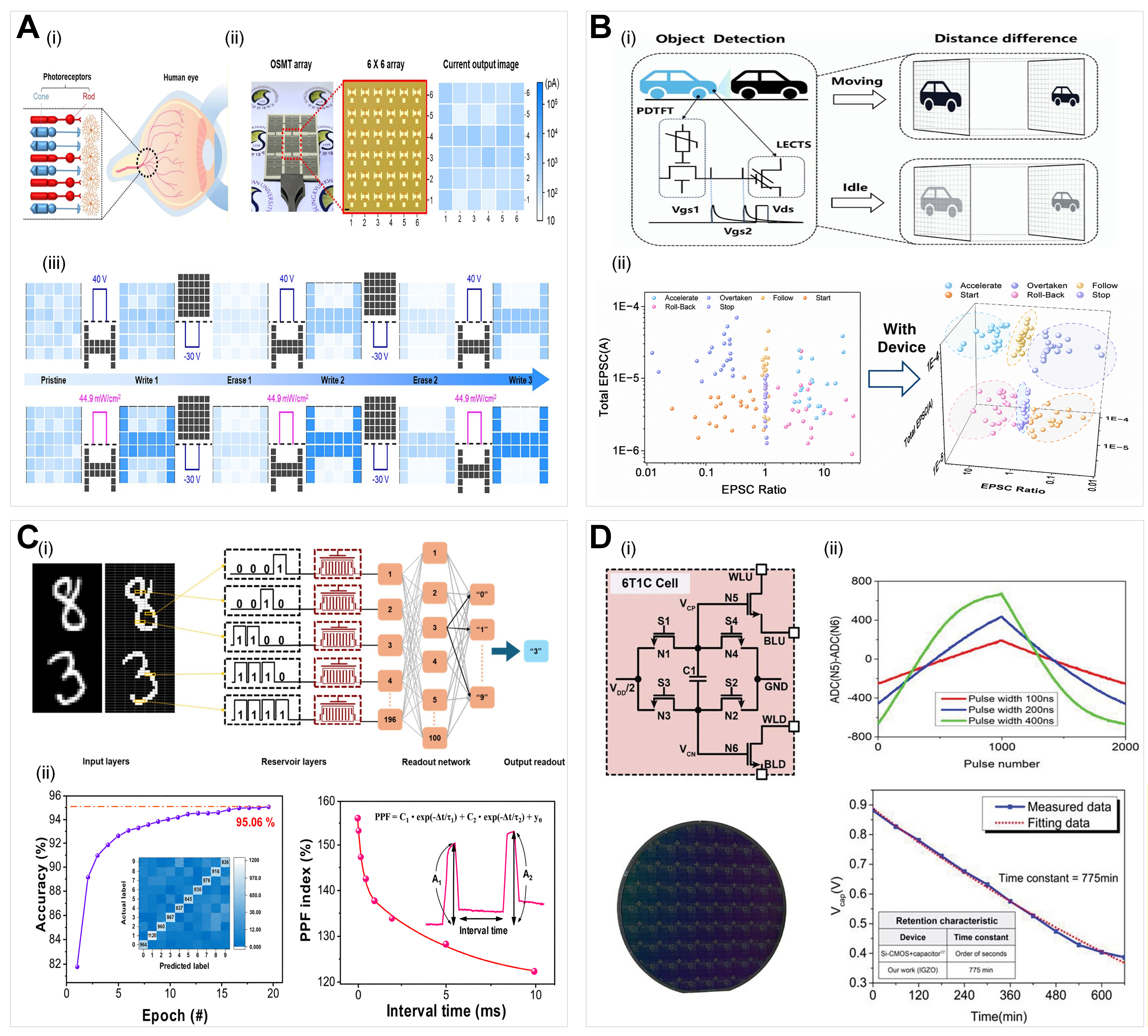
Figure 5. Integrated sensing-storage-computing systems and application scenarios. (A) Retina-inspired in-sensor image processing using contact-engineered IGZO optoelectronic synaptic memtransistors: (i) schematic of the biological retina and its photoreceptor arrangement; (ii) optical micrograph of the OSMT array, the corresponding 6 × 6 device array, and its initial current mapping; and (iii) evolution of the mapped image under successive electrical and optical write–erase operations, showing increased contrast between the target pattern and its background. Adapted from Ref.[128] under the CC BY 4.0 license. Copyright 2026, The Authors; (B) Tactile perception and robotic navigation based on FST encoding: (i) Schematic of the FST tactile encoding system. (ii) Real-time classification results for autonomous vehicle status detection and smart robotic navigation using the PDTFT-based SNN hardware. Adapted from Ref.[136] under the CC BY 4.0 license. Copyright 2025, The Authors; (C) RC for handwritten digit recognition: (i) Architecture of the RC system using IGZO-based leaky 2T dynamic random-access memory (DRAM) nodes as the physical reservoir. (ii) Confusion matrix showing the recognition results for the MNIST pattern recognition task. Reprinted with permission[141]. Copyright 2024, American Chemical Society; (D) Analog CIM and on-chip training: (i) Circuit topology of the 6T1C synaptic cell consisting of n-type IGZO TFTs and a storage capacitor, alongside a photograph of the fabricated 8-inch wafer. (ii) Synaptic weight update curves (potentiation and depression) and memory retention characteristics of the single 6T1C device. Adapted from Ref.[147] under the CC BY 4.0 license. Copyright 2023, The Authors. IGZO: Indium gallium zinc oxide; OSMT: optoelectronic synaptic memtransistor; FST: first-spike-timing; PDTFT: pressure-sensitive dual-TFT; SNN: spiking neural network; RC: reservoir computing; 2T: two-transistor; DRAM: dynamic random-access memory; MNIST: Modified National Institute of Standards and Technology; CIM: in-memory computing; TFTs: thin-film transistors; LECTS: light-electric coupling synaptic transistor; EPSC: excitatory postsynaptic current; PPF: paired-pulse facilitation; WLU: word line upper; BLU: bit line upper; GND: ground; WLD: word line lower; BLD: bit line lower; ADC: analog-to-digital conversion.
Li et al. further demonstrated an a-IGZO-based optoelectronic nociceptive device that generated nonlinear responses to increasing stimulus intensity and was coupled to an end-effector retraction operation with a reported response time below 10 ms[81]. This result illustrates the potential of sensor-level threshold responses for reducing control latency, although the overall response also depends on the associated readout and actuation circuitry. In-sensor a-IGZO devices can therefore combine optical sensing with temporal conductance modulation, but their broader use remains limited by spectral range, recovery dynamics, device variability, and system-level integration.
Near-sensor computing
Near-sensor computing places signal-processing circuits adjacent to the sensor rather than within the sensing element itself. In flexible health-monitoring systems, this arrangement can perform amplification, filtering, event detection, or feature extraction before wireless transmission, thereby reducing the amount of raw physiological data sent to a remote processor. Its effectiveness depends on the power consumption, mechanical compatibility, and parameter uniformity of both the sensor and the local processing circuits.
Human physiological signals [such as electroencephalography (EEG) and electromyography (EMG)] are typically characterized by weak amplitudes (ranging from microvolts to millivolts, e.g., 10 μV to 5 mV)[129], low frequencies, and susceptibility to motion interference. Because conventional rigid readout circuits cannot conform readily to skin deformation, the large-area uniformity and mechanical compatibility of a-IGZO TFTs make them promising building blocks for flexible front-end amplification circuits[130]. Particularly for analog circuits such as differential amplifiers, the consistency of device parameters (such as threshold voltage and mobility μ) is crucial. The all-photolithographic integration process recently developed by Li et al. successfully controlled the deviation of device parameters within the array to less than 5%, providing a solid hardware foundation for high-performance flexible analog front-end circuits[22]. On this basis, Ishida et al. designed a pseudo-complementary metal-oxide-semiconductor (CMOS)-based operational amplifier with a-IGZO TFTs on a flexible film, successfully achieving a 22.5 dB open-loop gain and a 31 kHz gain-bandwidth product, enabling weak bioelectric signals to be amplified directly to levels recognizable by back-end digital logic[131]. Zhao et al. further developed a unipolar a-IGZO TFT amplifier circuit with a parallel bootstrap capacitor, achieving an exceptional gain of 43.5 dB for bio-signal sensing applications, demonstrating excellent robustness for physiological monitoring[132].
Beyond simple signal amplification, near-sensor computing modules must also undertake feature extraction tasks. Shim et al. developed an all-rubber-based “cognitive skin”, integrating stretchable a-IGZO synaptic transistor arrays directly at the back-end of multi-channel tactile sensors. The system cleverly utilizes the exponential current-voltage characteristics of a-IGZO devices in the subthreshold region to construct high-pass filters (cutoff frequency < 1 Hz), effectively filtering out baseline drift noise caused by slow skin deformation[19]. Yuan et al. further constructed an artificial tactile perception system with spatio-temporal recognition capabilities, utilizing the STP of synaptic transistors to encode temporal signals generated by sliding, achieving material and pattern classification directly at the edge[133]. By natively decoding these complex spatio-temporal tactile patterns locally, the near-sensor computing module substantially reduces the volume of raw sensory data that needs to be transmitted to central processors, providing an energy-efficient approach for flexible electronic skin.
To compress data transmission volume to the extreme, near-sensor computing modules based on a-IGZO have further introduced the “event-driven” mechanism of the biological nervous system. In this architecture, synaptic devices are configured as integrate-and-fire (IF) neuron models, sending pulse signals to the back-end only when the cumulative intensity of the input signal exceeds a set threshold. Utilizing the unipolar switching characteristics of a-IGZO transistors, Lebanov et al. developed flexible IF neuron circuits for healthcare applications[134]. These circuits accumulate input signals and generate an output spike only after the membrane-like voltage exceeds a defined threshold, allowing infrequent or high-amplitude events to be encoded into sparse pulses. This operating principle is relevant to anomaly-triggered physiological monitoring, although its effect on complete-system battery life requires evaluation together with the sensor, wireless transmitter, and peripheral circuits.
The advantages of near-sensor computing also extend to complex spatiotemporal feature extraction, reducing reliance on energy-intensive ADCs. To achieve seamless continuous-to-discrete signal conversion, Qiao et al. constructed 1T1M-based universal oscillating units to serve as artificial sensory neurons, dynamically translating analog stimuli into highly compressed discrete spike trains[135]. Extending neuromorphic perception toward tactile sensing, Cai et al. developed a neuromorphic framework that integrates IGZO-based first-spike-timing (FST) tactile encoders with coupling-enhanced transistor synapses [Figure 5B(i)]. This architecture can efficiently convert continuous pressure stimuli into precise FST spike patterns, thereby providing an energy-efficient sensory front-end for downstream spiking neural networks (SNNs). When applied to spatiotemporal tactile-feedback tasks, including autonomous vehicle status detection and intelligent robotic navigation [Figure 5B(ii)], the system achieved high recognition accuracies of 98.4% and 98.2%, respectively, while reducing network training time by 90.9%[136]. In the visual domain, Song et al. proposed an artificial optoelectronic synapse utilizing a source-sharing circuitry design. Under dynamic irradiation, the device intrinsically integrates and decodes temporal light patterns, proving that a-IGZO circuitry can perform complex feature extraction directly at the sensory terminal before central routing[137].
Furthermore, near-sensor computing proves exceptionally effective in complex environmental chemical monitoring. Addressing the poor selectivity of traditional gas sensors, Chu et al. constructed a power-efficient gas-sensing synaptic diode based on a lateral pentacene/a-IGZO p-n junction[138]. When exposed to the target environment, different gas molecules (such as NO2 and NH3) act as distinct “chemical dopants” adsorbing at the organic/inorganic interface. This dynamic adsorption not only modulates the channel conductance but also regulates the update rate of synaptic weights (i.e., the learning rate). Inspired by the signal-processing behavior of the biological olfactory system, the device integrates gas sensing and synaptic processing within a single heterojunction platform, enabling the direct discrimination of mixed gases at the sensing node and providing a promising hardware solution for highly selective flexible electronic noses[138]. Near-sensor a-IGZO circuits can therefore perform local amplification, filtering, spike encoding, and sensory feature extraction. Their main advantages are reduced data transmission and compatibility with large-area flexible electronics, whereas circuit gain, device uniformity, mechanical drift, and peripheral power remain important system-level constraints.
RC
RC is particularly suited to temporal inputs that require nonlinear transformation and short-term memory, such as physiological waveforms, motion sequences, and speech. Unlike recurrent neural networks trained through backpropagation through time, RC uses a fixed nonlinear reservoir and trains only the readout layer. This reduces training complexity, although the performance still depends on the reservoir dynamics, input encoding, and stability of the readout states[139].
At the physical implementation level, the migration behavior of electrolyte ions or the charge trapping/release process of interface defects in a-IGZO synaptic transistors endows the devices with natural “fading memory” characteristics, which are core elements for building a physical reservoir. Yang et al. used the ionic relaxation of an EDL-coupled InGaZnO artificial synapse as a time-multiplexed physical reservoir. The device provided nonlinear fading-memory states, while the spoken-digit classification was performed using a trained readout layer. Under the reported conditions, the system achieved 100% accuracy, with an average device power of approximately 9.3 nW and an estimated energy of approximately 1.9 nJ per reservoir state[140].
Furthermore, in RC, precisely manipulating the retention time to achieve fading memory is crucial for matching the timescale of dynamic sequential inputs. To meet this requirement, Jang et al. developed a physical reservoir based on leaky two-transistor (2T) DRAM nodes utilizing nanometer-thick a-IGZO films [Figure 5C(i)]. By exploiting the controllable retention loss and PPF behavior of the 2T DRAM, the system efficiently mapped time-varying inputs into high-dimensional reservoir states through a 4-bit pulse scheme. When applied to handwritten digit recognition [Figure 5C(ii)], the framework achieved a high recognition accuracy of 95.06% within only 20 training epochs, demonstrating its potential for fast and energy-efficient temporal information processing[141].
To cope with more complex, higher-bandwidth scenarios, RC systems are evolving toward optoelectronic multimodal directions, using the recombination dynamics of photo-generated carriers instead of slow ion migration. Cui et al. designed a bioinspired in-materia analog photoelectronic RC system. By utilizing a receptive field-inspired encoding scheme and the intrinsic dynamics of photogenerated carriers, this system achieved over 90% recognition accuracy across four distinct human motion datasets. Remarkably, it verified falling behavior recognition with an exceptionally low energy consumption of ~45.78 μJ per action, significantly outperforming traditional vision processing hardware[142]. Fu et al. synthesized IGZO/PVP composite nanofiber neuromorphic transistors. This unique nanofiber network constructed a highly efficient reservoir for spatiotemporal visual tasks, achieving 92.86% accuracy in hand gesture recognition with a microscopic energy footprint of just 49 pJ per reservoir state[88].
In flexible implementations, changes in device response caused by mechanical deformation may alter the reservoir states. Zhang et al. showed that the recognition performance of a flexible RC system could be recovered after bending by retraining only the linear readout layer[33]. This approach does not eliminate mechanically induced drift, but it provides a relatively simple means of compensating for reproducible changes in reservoir response. Overall, a-IGZO devices offer fading memory and nonlinear dynamics suitable for temporal processing, although task performance remains sensitive to relaxation time, environmental drift, input encoding, and readout-layer training.
CIM
CIM reduces repeated data transfer between separate memory and processing units by performing multiply–accumulate operations within or close to the memory array[143]. In analog crossbars, multiplication is represented by conductance-dependent current and summation by current accumulation along shared lines. However, practical CIM systems still require programming, control, sensing, and data-conversion circuits, and therefore do not eliminate all data-movement or peripheral-circuit overhead. 1T1R arrays for resistive memories, 2T1C and 3T1C eDRAM cells, and modified 6T SRAM cells for computing-in-memory applications[143]. In these structures, a TFT provides cell selection, programming-current control, or charge isolation, depending on the memory architecture.
Compared with two-terminal memristors, three-terminal a-IGZO synaptic transistors separate gate-controlled programming from source–drain readout, allowing more controllable multilevel updates and reduced read disturbance. Their larger cell area and wiring overhead reduce integration density, whereas memristors offer compact, nonvolatile cross-point storage but often suffer from nonlinear or asymmetric updates, device and cycle variability, and sneak-path currents[144]. Thus, a-IGZO transistors favor precise weight control and active-matrix addressing, while memristors favor high-density integration and nonvolatile retention.
In passive resistive-memory crossbars, sneak-path currents reduce the read margin and can restrict practical array scaling. Active 1T1R arrays address this problem by using a transistor to isolate unselected cells[145,146]. In such configurations, the a-IGZO TFT primarily serves as an access device rather than the analog weight-storage element. This improves array selectivity but does not directly use the transistor’s own multilevel synaptic characteristics.
To further avoid the inherent non-idealities of memristors (such as nonlinear writing and asymmetry), the capacitive in-memory computing (C-CIM) paradigm, based on charge retention in capacitors, has received extensive attention. In this architecture, synaptic weights are stored on capacitors as analog voltages rather than relying on resistive switching of materials. Pioneering this domain, Won et al. performed a device-algorithm co-optimization for an on-chip trainable capacitor-based synaptic device utilizing IGZO TFTs, ensuring highly robust weight retention [Figure 5D(i) and (ii)][147]. Building upon this approach, Kang et al. designed an advanced analog neuromorphic on-chip training system based on an IGZO TFT 6T1C synaptic memory structure. Exploiting the extremely low leakage current of IGZO, they achieved a 10,000-fold enhanced retention time. This 6T1C architecture delivered an average of 367 distinct analog states with an extremely high R-squared linearity of 0.99, enabling the system to conduct successful analog on-chip training with an accuracy of 97.1% on the MNIST dataset[148]. Furthermore, seeking to overcome the density and leakage bottlenecks of traditional CMOS embedded DRAM, Kim et al. proposed a highly efficient compute-in-memory array design using 3T-based stacked hybrid IGZO/Si eDRAM cells. This vertical integration harnesses the exceptionally long retention time of IGZO (> 100 s) to drastically minimize refresh cycles while significantly increasing memory cell density for demanding computational workloads[149].
However, deploying CIM architectures on flexible electronics faces severe reliability challenges due to inherent device variations. Systematic simulation studies by Park et al. showed that spatial variations and threshold voltage drift of IGZO TFTs within the array critically compromise the consistency of analog VMM operations. Since analog computing relies heavily on uniform device I-V characteristics, this D2D variation directly translates into systematic errors. Their simulations quantitatively demonstrated that extensive threshold voltage fluctuations profoundly degrade the inference accuracy of SNNs[150]. To address these limitations, the same group subsequently developed high-performance IGZO synapse arrays using an ITO floating gate. This architecture significantly suppressed charge leakage and minimized D2D variations, ultimately achieving a 98.31% MNIST inference accuracy in an 8 × 8 array SNN simulation[28]. Beyond stabilizing synaptic weights, robust spiking neurons are essential for complete flexible SNN hardware. To this end, Lebanov et al. proposed fully flexible IF neuron circuits based exclusively on unipolar IGZO TFTs. Capitalizing on a-IGZO’s ultra-low leakage, these circuits effectively suppressed current drift and maintained highly stable membrane potential integration, establishing a crucial hardware foundation for highly reliable flexible SNNs[134].
a-IGZO TFTs are therefore attractive for active-matrix addressing, low-leakage charge storage, and controllable analog weight updates in CIM circuits. Their larger cell area relative to two-terminal memories, together with array nonuniformity, peripheral-circuit overhead, and strain-induced parameter drift, remains a limitation for high-density flexible integration. Further progress requires coordinated optimization of the memory cell, access transistor, interconnects, and training algorithm.
CONCLUSION AND OUTLOOK
Flexible a-IGZO synaptic transistors have progressed from reproducing individual forms of synaptic plasticity to supporting sensing, RC, and CIM. Advances in channel engineering, functional dielectrics, multi-gate structures, and vertical integration have expanded both their operating mechanisms and potential applications. Nevertheless, the transition from isolated devices to reliable flexible circuits and systems remains incomplete. The central question is no longer whether a single transistor can exhibit additional synaptic behaviors, but whether its conductance states can be written, retained, and read reproducibly across an array during prolonged electrical operation and mechanical deformation. Addressing this question requires coordinated progress in film processing, weight storage, array integration, and system validation.
The first challenge concerns the quality and uniformity of a-IGZO films fabricated within the limited thermal budget of flexible substrates. Polymer surfaces generally exhibit greater roughness than rigid substrates, even after planarization. Depositing a thin a-IGZO channel on such a surface can increase interface scattering and produce spatial variations in threshold voltage and subthreshold swing. These variations are particularly detrimental to analog neuromorphic arrays, in which transistor nonuniformity directly affects the accuracy of stored weights and matrix operations[151,152]. Meanwhile, insufficient film densification and residual weakly bonded oxygen under low-temperature processing can increase the density of subgap states and aggravate bias- and illumination-induced instability. Localized energy-delivery methods provide possible routes around this thermal constraint. Ultraviolet laser annealing and intense pulsed-light treatment, for example, can improve a-IGZO transistor characteristics without uniformly heating the substrate[153,154]. Combined with substrate planarization, buffer layers, and interface passivation, these techniques may improve both film quality and interface uniformity. The near-term priority is to establish process windows that reduce the distributions of electrical and synaptic parameters across large areas, rather than optimizing only the performance of representative devices.
Even with improved material uniformity, stable and energy-efficient weight storage remains difficult because programming energy, update linearity, and retention are closely coupled. EGTs can operate at low voltages owing to their high EDL capacitance, but spontaneous ion redistribution often causes conductance relaxation. This behavior is useful for STP and RC but limits long-term weight storage. Charge-trapping structures generally offer longer retention, whereas carrier injection across an energy barrier requires higher programming fields and may result in nonlinear or asymmetric weight updates. The metastability of oxygen-vacancy-related states in a-IGZO can introduce additional drift during repeated operation. Controlled ion-migration barriers, hybrid dielectric structures, interface-engineered charge-trapping layers, and ferroelectric coupling offer possible means of adjusting this balance[71,85], although none should be assumed to eliminate all three limitations. Future studies should therefore report energy per update, dynamic range, linearity, symmetry, retention, and endurance under consistent pulse and readout conditions. Their dependence on mechanical strain must also be evaluated, because a weight-storage mechanism that is stable on a rigid substrate may not preserve the same update trajectory during repeated deformation.
Reliable weight storage at the device level is necessary but insufficient for scalable flexible arrays. D2D variations in threshold voltage and conductance-update behavior accumulate across an array and produce systematic errors during analog vector–matrix multiplication. Simulations of IGZO neuromorphic systems have shown that threshold-voltage variation can reduce inference accuracy, while floating-gate engineering can suppress leakage and improve array uniformity[28,150]. Flexible implementation introduces further failure mechanisms, including interconnect resistance drift, contact degradation, strain localization, fatigue at vias or layer boundaries, and environment-induced threshold-voltage drift caused by ambient oxygen and moisture[155]. Read–write crosstalk and parasitic currents also become more important as array dimensions increase. Active selection, separated read and write terminals, array-level calibration, and variation-aware programming can mitigate electrical errors. Neutral-plane placement and island–bridge layouts can reduce strain in active regions and interconnects[4], whereas ultrathin organic/inorganic encapsulation, such as parylene-C/AlOx stacks, can limit gas permeation without severely restricting device bendability[156]. Low-temperature vertical integration may further increase density without exceeding the substrate thermal budget. Although the established manufacturing infrastructure for IGZO display backplanes provides a useful basis for large-area fabrication[157], it does not by itself demonstrate the scalability of analog synaptic arrays. The immediate goal should be to evaluate statistically meaningful arrays in terms of device yield, parameter distributions, write disturbance, interconnect resistance, weight drift, and computational accuracy throughout repeated programming and bending cycles.
At the circuit and system levels, device performance must be preserved after integration with neurons, selectors, sensors, and peripheral control circuits. IGZO-based capacitive memory cells and flexible IF circuits have demonstrated the feasibility of circuit-level weight storage and neuronal processing[134,147-149]. However, many reported neuromorphic functions still rely on individual devices, small arrays, or software simulations using selected device characteristics. In a complete flexible system, device variation, sensor drift, circuit noise, mechanical deformation, data-conversion overhead, and routing power occur simultaneously. Multimodal sensing further introduces cross-sensitivity and common-mode interference that cannot be addressed solely by adding more responsive materials. Differential readout, multi-gate regulation, and local preprocessing may improve signal separation, whereas the heterogeneous integration of a flexible sensing–computing front end with a rigid CMOS control back end offers a practical intermediate strategy. Hardware–software co-design should use experimentally measured parameter distributions and time-dependent drift to guide calibration, retraining, and fault-tolerant learning[158]. System-level demonstrations should report not only task accuracy but also latency, total energy consumption, and performance stability after prolonged programming, inference, environmental exposure, and mechanical cycling.
These priorities are sequentially connected: film and interface uniformity determine device reproducibility, stable weight storage enables reliable circuits, and mechanically robust arrays provide the basis for system-level evaluation. The most urgent step is therefore not to demonstrate additional isolated synaptic functions, but to validate reproducible array-level learning and inference under prolonged electrical and mechanical operation.
DECLARATIONS
Authors’ contributions
Made substantial contributions to the conception and design of this review, as well as figure preparation and manuscript writing: Xiao Q
Provided technical support, analyzed and discussed the results: Guo X, Song R
Supervised the overall work, provided resource support, and reviewed and edited the manuscript: Liu M, Li J
Availability of data and materials
Not applicable.
AI and AI-assisted tools statement
During the preparation of this manuscript, OpenAI ChatGPT-5 (GPT-5, released 2025-08-07) was used for language translation and editing. The image-generation capability of OpenAI ChatGPT was also used to assist in preparing the hand illustrations in Figure 1 and the graphical abstract. The AI tool did not influence the study design, literature selection, data analysis, interpretation, conclusions, or any other scientific content of the work. All authors reviewed and verified the AI-assisted textual and graphical content and take full responsibility for the accuracy, integrity, and final content of the manuscript.
Financial support and sponsorship
This study was financially supported by the National Natural Science Foundation of China Project (62404050, 62574124) and the Shanghai Science and Technology Commission (25ZR1401120).
Conflicts of interest
All authors declared that there are no conflicts of interest.
Ethical approval and consent to participate
Not applicable.
Consent for publication
Not applicable.
Copyright
© The Author(s) 2026.
REFERENCES
1. Someya, T.; Bao, Z.; Malliaras, G. G. The rise of plastic bioelectronics. Nature 2016, 540, 379-85.
2. Liu, L.; Gu, Y.; Li, S.; Liu, H.; Jia, X.; Xu, Y. Skin-inspired flexible multimodal sensor with decoupled force–temperature–triboelectric perception for human-like tactile intelligence. Chem. Eng. J. 2026, 527, 171990.
3. Sun, X.; Sun, J.; Zheng, S.; et al. A sensitive piezoresistive tactile sensor combining two microstructures. Nanomaterials 2019, 9, 779.
5. Mehonic, A.; Kenyon, A. J. Brain-inspired computing needs a master plan. Nature 2022, 604, 255-60.
6. Horowitz, M. 1.1 Computing’s energy problem (and what we can do about it). In Proceedings of the 2014 IEEE International Solid-State Circuits Conference (ISSCC), San Francisco, USA. Feb 09-13, 2014. IEEE; 2014. pp 10-4.
8. Jang, H.; Lee, J.; Beak, C. J.; Biswas, S.; Lee, S. H.; Kim, H. Flexible neuromorphic electronics for wearable near-sensor and in-sensor computing systems. Adv. Mater. 2025, 37, e2416073.
9. Petti, L.; Münzenrieder, N.; Vogt, C.; et al. Metal oxide semiconductor thin-film transistors for flexible electronics. Appl. Phys. Rev. 2016, 3, 021303.
10. Gelinck, G. H.; Huitema, H. E.; van Veenendaal, E.; et al. Flexible active-matrix displays and shift registers based on solution-processed organic transistors. Nat. Mater. 2004, 3, 106-10.
11. Kim, Y. C.; Lee, S. J.; Oh, I.; Seo, S.; Kim, H.; Myoung, J. Bending stability of flexible amorphous IGZO thin film transistors with transparent IZO/Ag/IZO oxide–metal–oxide electrodes. J. Alloys. Compd. 2016, 688, 1108-14.
12. Jang, H.; Kim, G.; Yoon, S. Analysis of mechanical and electrical origins of degradations in device durability of flexible InGaZnO thin-film transistors. ACS. Appl. Electron. Mater. 2020, 2, 2113-22.
13. Wang, X.; Qi, L.; Yang, H.; Rao, Y.; Chen, H. Stretchable synaptic transistors based on the field effect for flexible neuromorphic electronics. Soft. Sci. 2023, 3, 15.
14. Tavasli, A.; Atila, D. T.; Faraji, S.; Majewski, L. A.; Trabzon, L. Organic phototransistors and their applications as artificial synapses. Sens. Actuators. A. Phys. 2024, 371, 115311.
15. Nomura, K.; Ohta, H.; Takagi, A.; Kamiya, T.; Hirano, M.; Hosono, H. Room-temperature fabrication of transparent flexible thin-film transistors using amorphous oxide semiconductors. Nature 2004, 432, 488-92.
16. Fortunato, E.; Barquinha, P.; Martins, R. Oxide semiconductor thin-film transistors: a review of recent advances. Adv. Mater. 2012, 24, 2945-86.
17. Hosono, H. Ionic amorphous oxide semiconductors: material design, carrier transport, and device application. J. Non. Cryst. Solids. 2006, 352, 851-8.
18. Kamiya, T.; Nomura, K.; Hosono, H. Present status of amorphous In-Ga-Zn-O thin-film transistors. Sci. Technol. Adv. Mater. 2010, 11, 044305.
19. Shim, H.; Jang, S.; Thukral, A.; et al. Artificial neuromorphic cognitive skins based on distributed biaxially stretchable elastomeric synaptic transistors. Proc. Natl. Acad. Sci. U. S. A. 2022, 119, e2204852119.
20. Chen, J.; Chiu, Y.; Chiang, T.; Liu, P. Synaptic plasticity enhancement by supercritical fluid processed a-IGZO transistors for robust image recognition applications. Appl. Surf. Sci. 2025, 697, 163028.
21. Wan, X.; Yang, Y.; Feng, P.; Shi, Y.; Wan, Q. Short-term plasticity and synaptic filtering emulated in electrolyte-gated IGZO transistors. IEEE. Electron. Device. Lett. 2016, 37, 299-302.
22. Li, J.; Lei, Y.; Wang, Z.; et al. High-density artificial synapse array consisting of homogeneous electrolyte-gated transistors. Adv. Sci. 2024, 11, e2305430.
23. Yoon, S. J.; Park, J. T.; Lee, Y. K. The neuromorphic computing for biointegrated electronics. Soft. Sci. 2024, 4, 30.
24. Guo, L. Q.; Zhu, L. Q.; Ding, J. N.; Huang, Y. K. Paired-pulse facilitation achieved in protonic/electronic hybrid indium gallium zinc oxide synaptic transistors. AIP. Adv. 2015, 5, 087112.
25. Abbott, L. F.; Nelson, S. B. Synaptic plasticity: taming the beast. Nat. Neurosci. 2000, 3 Suppl, 1178-83.
26. Dai, S.; Zhao, Y.; Wang, Y.; et al. Recent advances in transistor‐based artificial synapses. Adv. Funct. Mater. 2019, 29, 1903700.
27. Wan, C. J.; Liu, Y. H.; Zhu, L. Q.; Feng, P.; Shi, Y.; Wan, Q. Short-term synaptic plasticity regulation in solution-gated indium-gallium-zinc-oxide electric-double-layer transistors. ACS. Appl. Mater. Interfaces. 2016, 8, 9762-8.
28. Park, J.; Yun, Y.; Bae, S.; Jang, Y.; Shin, S.; Lee, S. Y. High-performance synapse arrays for neuromorphic computing via floating gate-engineered IGZO synaptic transistors. Adv. Sci. 2025, 12, e2500568.
29. Zhu, L.; Li, S.; Lin, J.; et al. Ultra-low power IGZO optoelectronic synaptic transistors for neuromorphic computing. Sci. China. Inf. Sci. 2024, 67, 3966.
30. Yang, D.; Chen, H.; Tang, Z.; Sun, Q.; Tang, X. Optoelectronic synapses based on IGZO/Bi3.25La0.75Ti3O12 heterojunctions for human brain learning mechanism simulation. J. Semicond. 2026, 47, 012403.
31. Gokmen, T.; Vlasov, Y. Acceleration of deep neural network training with resistive cross-point devices: design considerations. Front. Neurosci. 2016, 10, 333.
32. Burr, G. W.; Shelby, R. M.; Sebastian, A.; et al. Neuromorphic computing using non-volatile memory. Adv. Phys. X. 2017, 2, 89-124.
33. Zhang, S.; Zhu, J.; Qiu, R.; Liu, D.; Ren, Q.; Zhang, M. Flexible tunable-plasticity synaptic transistors for mimicking dynamic cognition and reservoir computing. Adv. Mater. 2025, 37, e2418418.
34. Kwak, T.; Kim, M.; Lee, W.; et al. Ultra-large dynamic range synaptic indium gallium zinc oxide transistors. Appl. Mater. Today. 2022, 29, 101648.
35. Li, Y.; Cai, W.; Tao, R.; et al. Flexible and energy-efficient synaptic transistor with quasi-linear weight update protocol by inkjet printing of orientated polar-electret/high-k oxide composite dielectric. ACS. Appl. Mater. Interfaces. 2024, 16, 19271-82.
36. Wen, S.; Chen, L.; Li, J.; Zhang, J. Design of 3-D interface in synaptic transistors with attojoule power by electrospinning aligned nanofibers for neuromorphic computing. IEEE. Trans. Electron. Devices. 2023, 70, 6644-50.
37. Wen, S.; Li, J.; Wang, Z.; Zhang, Z.; Zhang, J. Low-power and high PPF feature synaptic transistors with 3D interface based on SnO2 nanofibers for neuromorphic application. Appl. Phys. Lett. 2023, 123, 043503.
38. Zhang, W.; Li, J.; Cheng, L.; et al. Synaptic transistor arrays based on PVA/lignin composite electrolyte films. IEEE. Trans. Electron. Devices. 2023, 70, 3245-50.
39. Suo, Z.; Ma, E. Y.; Gleskova, H.; Wagner, S. Mechanics of rollable and foldable film-on-foil electronics. Appl. Phys. Lett. 1999, 74, 1177-9.
40. Shim, H.; Sim, K.; Ershad, F.; et al. Stretchable elastic synaptic transistors for neurologically integrated soft engineering systems. Sci. Adv. 2019, 5, eaax4961.
41. Ajayan, J.; Sreejith, S.; Kumari, N. A.; Manikandan, M.; Sen, S.; Kumar, M. Amorphous indium gallium zinc oxide thin film transistors (a-IGZO-TFTs): exciting prospects and fabrication challenges. Microelectron. Eng. 2025, 298, 112327.
42. Li, L.; Shao, Y.; Wang, X.; et al. Flexible femtojoule energy-consumption In-Ga-Zn-O synaptic transistors with extensively tunable memory time. IEEE. Trans. Electron. Devices. 2020, 67, 105-12.
43. Choi, H. S.; Han, D. H.; Jeong, H. W.; et al. High-performance annealing-free InGaZnOx thin film transistors by thermal ALD. Appl. Phys. Lett. 2026, 128, 043505.
44. Moreira, M.; Carlos, E.; Dias, C.; et al. Tailoring IGZO composition for enhanced fully solution-based thin film transistors. Nanomaterials 2019, 9, 1273.
45. Everaerts, K.; Zeng, L.; Hennek, J. W.; et al. Printed indium gallium zinc oxide transistors. Self-assembled nanodielectric effects on low-temperature combustion growth and carrier mobility. ACS. Appl. Mater. Interfaces. 2013, 5, 11884-93.
46. Zhang, Y.; He, G.; Wang, L.; Wang, W.; Xu, X.; Liu, W. Ultraviolet-assisted low-thermal-budget-driven α-InGaZnO thin films for high-performance transistors and logic circuits. ACS. Nano. 2022, 16, 4961-71.
47. Jang, Y.; Park, J.; Kang, J.; Lee, S. Amorphous InGaZnO (a-IGZO) synaptic transistor for neuromorphic computing. ACS. Appl. Electron. Mater. 2022, 4, 1427-48.
48. Cha, D.; Pi, J.; Lee, S. Effects of programming-pulse frequency on synaptic characteristics of amorphous IGZO thin-film transistors with defective gate oxides. IEEE. Access. 2026, 14, 27665-74.
49. Belmonte, A.; Oh, H.; Rassoul, N.; et al. Capacitor-less, long-retention (>400 s) DRAM cell paving the way towards low-power and high-density monolithic 3D DRAM. In Proceedings of the 2020 IEEE International Electron Devices Meeting (IEDM), San Francisco, USA. Dec 12-18, 2020. IEEE; 2020. pp 28.2.1-4.
50. Choi, W. S.; Song, M. S.; Kim, H.; Kim, D. H. Conduction mechanism analysis of abrupt- and gradual-switching InGaZnO memristors. Micromachines 2022, 13, 1870.
51. Sagar, S.; Udaya, Mohanan. K.; Cho, S.; Majewski, L. A.; Das, B. C. Emulation of synaptic functions with low voltage organic memtransistor for hardware oriented neuromorphic computing. Sci. Rep. 2022, 12, 3808.
52. Hong, T.; Kim, Y.; Choi, S.; Lim, J. H.; Park, J. Exploration of chemical composition of In–Ga–Zn–O system via PEALD technique for optimal physical and electrical properties. Adv. Electron. Mater. 2023, 9, 2201208.
53. Chen, F.; Zhang, M.; Wan, Y.; Xu, X.; Wong, M.; Kwok, H. Advances in mobility enhancement of ITZO thin-film transistors: a review. J. Semicond. 2023, 44, 091602.
54. Jia, J.; Torigoshi, Y.; Kawashima, E.; Utsuno, F.; Yano, K.; Shigesato, Y. Amorphous indium-tin-zinc oxide films deposited by magnetron sputtering with various reactive gases: spatial distribution of thin film transistor performance. Appl. Phys. Lett. 2015, 106, 023502.
55. Kim, M. S.; Kim, H. T.; Yoo, H.; et al. Multifunctional oxygen scavenger layer for high-performance oxide thin-film transistors with low-temperature processing. ACS. Appl. Mater. Interfaces. 2021, 13, 31816-24.
56. Kim, H. G.; Lee, H. J.; Lee, K. M.; Kim, T. G. Improved mobility and bias stability of Hf-doped IGZO/IZO/Hf-doped IGZO thin-film transistor. J. Alloys. Compd. 2024, 981, 173587.
57. Chen, H.; Song, C.; Wu, J.; et al. Chloride modulation doping in dual-channel InGaZnO synaptic transistors: location-selective strategy for synaptic plasticity enhancement. ACS. Appl. Electron. Mater. 2025, 7, 11108-19.
58. Zhang, L.; Xu, Z.; Han, J.; et al. Resistive switching performance improvement of InGaZnO-based memory device by nitrogen plasma treatment. J. Mater. Sci. Technol. 2020, 49, 1-6.
59. Beom, K.; Kim, M.; Lee, H.; et al. Effect of nitrogen-doping on drain current modulation characteristics of an indium-gallium-zinc oxide thin-film transistor. Nanotechnology 2020, 31, 265201.
60. Kim, J.; Kim, Y.; Kwon, O.; et al. Modulation of synaptic plasticity mimicked in Al nanoparticle‐embedded IGZO synaptic transistor. Adv. Electron. Mater. 2020, 6, 1901072.
61. Choi, J. G.; Song, Y.; Baek, S.; Jang, J.; Park, S. Al nanoparticle-decorated metal oxide synaptic transistors for ultralow-energy neuromorphic computing with wide dynamic range. Adv. Sci. 2026, 13, e21321.
62. Kwak, K.; Park, K.; Han, J. S.; et al. Swiftly accessible retinomorphic hardware for in-sensor image preprocessing and recognition: IGZO-based neuro-inspired optical image sensor arrays with metallic sensitization island. Int. J. Extrem. Manuf. 2025, 7, 065504.
63. Yang, B. F.; Zhang, C.; Zhang, Z. H.; et al. An InGaZnO synaptic transistor using titanium-oxide traps at back channel for neuromorphic computing. IEEE. Trans. Electron. Devices. 2025, 72, 2943-8.
64. Chen, J.; Li, E.; Yan, Y.; et al. Flexible metal oxide synaptic transistors using biomass-based hydrogel as gate dielectric. J. Phys. D. Appl. Phys. 2019, 52, 484002.
65. Kim, S. H.; Cho, W. J. Lithography processable Ta2O5 barrier-layered chitosan electric double layer synaptic transistors. Int. J. Mol. Sci. 2021, 22, 1344.
66. Lee, D. H.; Park, H.; Cho, W. J. Nanowire-enhanced fully transparent and flexible indium gallium zinc oxide transistors with chitosan hydrogel gate dielectric: a pathway to improved synaptic properties. Gels 2023, 9, 931.
67. Wu, X.; Chen, S.; Moser, M.; et al. High performing solid‐state organic electrochemical transistors enabled by glycolated polythiophene and ion‐gel electrolyte with a wide operation temperature range from -50 to 110 °C. Adv. Funct. Mater. 2023, 33, 2209354.
68. Cho, K. G.; Cho, Y. K.; Kim, J. H.; Yoo, H. Y.; Hong, K.; Lee, K. H. Thermostable ion gels for high-temperature operation of electrolyte-gated transistors. ACS. Appl. Mater. Interfaces. 2020, 12, 15464-71.
69. Hoffmann, M.; Schroeder, U.; Schenk, T.; et al. Stabilizing the ferroelectric phase in doped hafnium oxide. J. Appl. Phys. 2015, 118, 072006.
70. Park, M. H.; Lee, Y. H.; Kim, H. J.; et al. Ferroelectricity and antiferroelectricity of doped thin HfO2-based films. Adv. Mater. 2015, 27, 1811-31.
71. Goh, Y.; Hwang, J.; Lee, Y.; Kim, M.; Jeon, S. Ultra-thin Hf0.5Zr0.5O2 thin-film-based ferroelectric tunnel junction via stress induced crystallization. Appl. Phys. Lett. 2020, 117, 242901.
72. Jariwala, D.; Marks, T. J.; Hersam, M. C. Mixed-dimensional van der Waals heterostructures. Nat. Mater. 2017, 16, 170-81.
73. Chen, T.; Zhan, S.; Li, B.; Hou, B.; Zhou, H. A low‐toxic colloidal quantum dots sensitized IGZO phototransistor array for neuromorphic vision sensors. Adv. Opt. Mater. 2024, 12, 2302451.
74. Zhu, L.; Li, S.; Shu, K.; et al. Visible-light responsive CdS-QDs modified InGaZnO synapse for biologically plausible color-to-gray conversion. Appl. Phys. Lett. 2024, 125, 033502.
75. Zhu, L.; Li, S.; Zhang, F.; et al. Bio-inspired P-type TeSeOx synaptic transistor based on multispectral sensing for neuromorphic visual multilevel nociceptor. Small. Methods. 2025, 9, e2401543.
76. Duan, H.; Liang, L.; Wu, Z.; Zhang, H.; Huang, L.; Cao, H. IGZO/CsPbBr3-nanoparticles/IGZO neuromorphic phototransistors and their optoelectronic coupling applications. ACS. Appl. Mater. Interfaces. 2021, 13, 30165-73.
77. Yang, J.; Kwak, H.; Lee, Y.; et al. MoS2-InGaZnO heterojunction phototransistors with broad spectral responsivity. ACS. Appl. Mater. Interfaces. 2016, 8, 8576-82.
78. Park, K.; Kang, B. H.; An, J. B.; et al. Endurable IGZO/SnSx/IGZO heterojunction phototransistor arrays for image sensors. ACS. Appl. Mater. Interfaces. 2025, 17, 3620-30.
79. Abubakr, M.; Pervez, M. H.; Rehmat, A.; et al. UV to NIR photodetection in lateral homojunction PN diode of WSe2 achieved via IGZO sputtering. J. Mater. Chem. C. 2025, 13, 8544-52.
80. Hou, Z.; Gao, S.; Shen, J.; Fan, J.; Zhong, Y.; Wu, D. Coplanar all-solid-state electrolyte-gated IGZO artificial synapses for neuromorphic computing applications. Semicond. Sci. Technol. 2025, 40, 065001.
81. Li, X.; Ji, X.; Yin, X.; et al. Electro‐optical InGaZnO synaptic transistor with solid state electrolyte for pain perception. Adv. Electron. Mater. 2025, 11, 2400356.
82. Jeong, H.; Ahn, D.; Park, S.; Ju, G.; Han, J.; Kim, Y. Visible light wavelength-dependent erasing in AOS-based charge trap TFTs for enhanced neuromorphic display performance. ACS. Appl. Electron. Mater. 2025, 7, 5463-72.
83. Jang, J.; Lee, J.; Bae, J.; Cho, S.; Kim, S. InGaZnO-based synaptic transistor with embedded ZnO charge-trapping layer for reservoir computing. Sens. Actuators. A. Phys. 2024, 373, 115405.
84. Cho, M. H.; Choi, C. H.; Seul, H. J.; Cho, H. C.; Jeong, J. K. Achieving a low-voltage, high-mobility IGZO transistor through an ALD-derived bilayer channel and a Hafnia-based gate dielectric stack. ACS. Appl. Mater. Interfaces. 2021, 13, 16628-40.
85. Kwon, O.; Lee, D. H.; Oh, S.; et al. Dynamic control of synaptic plasticity by competing ferroelectric and trap‐assisted switching in IGZO transistors with Al2O3/HfO2 dielectrics. Adv. Funct. Mater. 2026, 36, e13449.
86. Lee, S.; An, G.; Kim, D.; Lee, H.; Kim, S.; Kim, T. H. Energy efficient hybrid reservoir computing using Hf0.5Zr0.5O2 ferroelectric thin-film transistors with an integrated optically and electrically synaptic functions. Small 2025, 21, e2501276.
87. Jiang, S.; Cheng, S.; Yang, J.; Guo, X.; He, B.; He, G. Electrospinning‐driven IGZO nanofiber phototransistors bridging adaptive processing and recognition learning. Rare. Metals. 2026, 45, e70215.
88. Fu, C.; Pei, M.; Cui, H.; et al. IGZO/PVP composite nanofiber neuromorphic transistors with optoelectronic synapse emulation and reservoir computing. J. Phys. Chem. Lett. 2024, 15, 9585-92.
89. Fu, C.; Li, Z.; Li, Y.; et al. High-performance IGZO/In2O3 NW/IGZO phototransistor with heterojunctions architecture for image processing and neuromorphic computing. J. Mater. Sci. Technol. 2024, 196, 190-9.
90. Luo, S.; Fu, C.; Zhang, C.; et al. IGZO/InHfOx nanowires/IGZO phototransistor with persistent photoconductivity effect for intelligent visual perception application. IEEE. Trans. Electron. Devices. 2024, 71, 4745-50.
91. Jang, N.; Kwon, Y. H.; Seong, N. J.; Choi, K.; Yoon, S. M. Synergistic approaches to minimize device footprint and energy consumption in vertical-channel synapse transistors using an InGaZnO active layer via spacer engineering of HfO2. ACS. Appl. Mater. Interfaces. 2025, 17, 40788-97.
92. Sun, J.; Yu, W.; Zhang, J.; et al. In situ engineering of vertical indium gradients via sputtering kinetics for high-performance IGZO channel-all-around transistors. Nano. Lett. 2026, 26, 3899-906.
93. Hu, Z.; Dou, H.; Gan, J. B.; et al. An ultra‐robust memristor based on vertically aligned nanocomposite with highly defective vertical channels for neuromorphic computing. Adv. Funct. Mater. 2026, 36, e12719.
94. Na, J. W.; Hwang, Y. S.; Lee, I. S.; et al. Swing-tunable oxide thin-film transistors via electrohydrodynamic jet-printed parasitic conduction path. ACS. Appl. Mater. Interfaces. 2025, 17, 66876-88.
95. Sihn, S.; Chambers, W. L.; Abedin, M.; et al. Enhanced computational study with experimental correlation on I-V characteristics of tantalum oxide (TaOx) memristor devices in a 1T1R configuration. Small 2025, 21, e2310542.
96. Li, J. C.; Ma, Y. X.; Wu, S. H.; et al. 1-Selector 1-memristor configuration with multifunctional a-IGZO memristive devices fabricated at room temperature. ACS. Appl. Mater. Interfaces. 2024, 16, 17766-77.
97. Li, Y.; Liu, S.; Zheng, H.; et al. From planar to 3D: the evolution of complementary field-effect transistor for next-generation semiconductor nodes. Adv. Mater. 2026, 38, e73226.
98. Kim, H. W.; Kim, J. H.; Shin, D. H.; et al. Neuromorphic visual receptive field hardware with vertically integrated indium-gallium-zinc-oxide optoelectronic memristors over silicon neuron transistors. Adv. Mater. 2026, 38, e13907.
99. Shi, R.; Guo, S.; Wang, L.; et al. Monolithic 3D-integrated neuromorphic biosignal processor using hydrogen-controlled dual-gate TFTs on a flexible substrate. In Proceedings of the 2025 IEEE International Electron Devices Meeting (IEDM), San Francisco, USA. Dec 06-10, 2025. IEEE; 2025. p 1-4.
100. Park, J.; Oh, W. S.; Lee, J.; Oh, H. Improving endurance and thermal stability in IGZO-based ReRAM using an a-BN intermediate layer. J. Korean. Phys. Soc. 2025, 86, 522-8.
101. Xu, M.; Long, H.; Fu, C.; Mao, H.; Wan, C.; Wan, Q. A flexible thermal-coupled InGaZnO adaptive synapse. Appl. Phys. Lett. 2024, 124, 163502.
102. Kwak, H.; Lee, C.; Lee, C.; Noh, K.; Kim, S. Experimental measurement of ungated channel region conductance in a multi-terminal, metal oxide-based ECRAM. Semicond. Sci. Technol. 2021, 36, 114002.
103. Hu, Y.; Ho, T. S. P.; Lei, T.; Xia, Z.; Wong, M. Construction and application of a neuromorphic circuit with excitatory and inhibitory post-synaptic conduction channels implemented using dual-gate thin-film transistors. IEEE. Trans. Circuits. Syst. I. Regul. Pap. 2024, 71, 1582-9.
104. Wei, J.; Li, N.; Zhang, Y.; et al. Reliability analysis under bias stress and elevated temperature of dual-gate IGZO TFT. AIP. Adv. 2024, 14, 115122.
105. Liu, X.; Sun, C.; Guo, Z.; et al. A flexible dual-gate hetero-synaptic transistor for spatiotemporal information processing. Nanoscale. Adv. 2022, 4, 2412-9.
106. Xi, F.; Grenmyr, A.; Zhang, J.; et al. Heterosynaptic plasticity and neuromorphic boolean logic enabled by ferroelectric polarization modulated schottky diodes. Adv. Elect. Mater. 2023, 9, 2201155.
107. Qi, Y.; Tang, J.; Fan, S.; An, C.; Wu, E.; Liu, J. Dual interactive mode human-machine interfaces based on triboelectric nanogenerator and IGZO/In2O3 heterojunction synaptic transistor. Small. Methods. 2024, 8, e2301698.
108. Zhou, S. Y.; Li, B. B.; Wang, W. S.; Gong, B. C.; Di, J. K.; Zhu, L. Q. Bionic tactile-visual-morphic system based on oxide photoelectronic neuromorphic transistor and triboelectric nanogenerator. Front. Phys. 2026, 21, 024203.
109. Yang, T.; Kuo, D.; Tang, K. n-type Sn substitution in amorphous IGZO film by sol-gel method: a promoter of hall mobility up to 65 cm2/V·s. J. Non. Cryst. Solids. 2021, 553, 120503.
110. Park, E.; Jang, S.; Noh, G.; et al. Indium-gallium-zinc oxide-based synaptic charge trap flash for spiking neural network-restricted boltzmann machine. Nano. Lett. 2023, 23, 9626-33.
111. Zhu, Y.; Peng, B.; Zhu, L.; et al. IGZO nanofiber photoelectric neuromorphic transistors with indium ratio tuned synaptic plasticity. Appl. Phys. Lett. 2022, 121, 133502.
112. Belmonte, A.; Oh, H.; Subhechha, S.; et al. Tailoring IGZO-TFT architecture for capacitorless DRAM, demonstrating >103 s retention, >1011 cycles endurance and Lg scalability down to 14 nm. In Proceedings of the 2021 IEEE International Electron Devices Meeting (IEDM), San Francisco, USA. Dec 11-16, 2021. IEEE; 2021. pp 10.6.1-4.
113. An, J. B.; Park, K.; Lee, I. S.; et al. Retinocortical in-sensor neuromorphic vision platform for NIR-augmented artificial vision. Nat. Commun. 2026, 17, 4957.
115. Li, H. K.; Chen, T. P.; Liu, P.; et al. A light-stimulated synaptic transistor with synaptic plasticity and memory functions based on InGaZnOx–Al2O3 thin film structure. J. Appl. Phys. 2016, 119, 244505.
116. Gao, S.; Qiu, L.; Zhang, J.; Han, W.; Ramakrishna, S.; Long, Y. Persistent photoconductivity of metal oxide semiconductors. ACS. Appl. Electron. Mater. 2024, 6, 1542-61.
117. Jo, Y.; Lee, H.; Jeon, J.; et al. Enhanced visible-light response and optoelectronic properties of a-IGZO phototransistors with dye and PMMA blend heterojunctions. ACS. Appl. Electron. Mater. 2026, 8, 1716-25.
118. Liu, X.; Gui, Y.; Wang, Z.; et al. Robust optoelectronic dual-mode memristor enabled by ZnO/MoS2 heterojunction for synaptic bionics and in-memory computing. Sci. China. Inf. Sci. 2026, 69, 4674.
119. Pereira, M. E.; Deuermeier, J.; Martins, R.; Barquinha, P.; Kiazadeh, A. Unlocking neuromorphic vision: advancements in IGZO-based optoelectronic memristors with visible range sensitivity. ACS. Appl. Electron. Mater. 2024, 6, 5230-43.
120. Seo, T.; Yun, J.; Chung, Y. IGZO photonic-synaptic transistors with outstanding linearity by controlling oxygen vacancy for neuromorphic computing. In Proceedings of the 2023 7th IEEE Electron Devices Technology & Manufacturing Conference (EDTM), Seoul, Kerea. Mar 07-10, 2023. IEEE; 2023. p 1-3.
121. Mondal, R. K.; Kim, Y. J.; Kim, M. IGZO-based transparent optoelectronic synapse for stealth mode trajectory tracking and registration. Opt. Lett. 2025, 50, 3864-6.
122. Liang, K.; Wang, R.; Huo, B.; et al. Fully printed optoelectronic synaptic transistors based on quantum dot-metal oxide semiconductor heterojunctions. ACS. Nano. 2022, 16, 8651-61.
123. Li, S.; Yang, C.; Jia, L.; et al. A bio-inspired neuromorphic pressure afferent nerve based on fully inkjet-printed synaptic transistor. Appl. Phys. Lett. 2025, 127, 063301.
124. Franco, M.; Kiazadeh, A.; Deuermeier, J.; Lanceros-Méndez, S.; Martins, R.; Carlos, E. Inkjet printed IGZO memristors with volatile and non-volatile switching. Sci. Rep. 2024, 14, 7469.
125. Hou, Z.; Shen, J.; Zhong, Y.; Wu, D. Photonic-electronic modulated a-IGZO synaptic transistor with high linearity conductance modulation and energy-efficient multimodal learning. Micromachines 2025, 16, 517.
126. Wen, S.; Liu, Y.; Li, Y.; Xie, L.; Li, J.; Zhang, J. Dynamic hybrid visual-thermal multimodal perception neuromorphic devices based on defect modulation of electrospun nanofibers. Int. J. Extrem. Manuf. 2025, 7, 025506.
127. Yang, J.; Wang, B.; He, B.; et al. ALD-driven ultrathin IGZO neuromorphic transistors with defect-engineered 1/f noise for stable multimodal information encryption. J. Phys. Chem. Lett. 2026, 17, 772-9.
128. Kang, D.; Nam, S.; Nam, D.; et al. Retinomorphic visual processing enabled by contact-engineered IGZO optoelectronic synaptic memtransistors. Adv. Sci. 2026, e76218.
129. Webster, J. G. Medical instrumentation: application and design. John Wiley & Sons; 2009. https://books.google.com/books/about/Medical_Instrumentation_Application_and.html?id=ejuvtAEACAAJ. (accessed 2026-09-01).
130. Cheng, L.; Guo, A.; Li, J.; et al. Scalable integration of heterogeneous active surface electromyography electrode arrays for neural interfaces. Int. J. Extrem. Manuf. 2026, 8, 015504.
131. Ishida, K.; Shabanpour, R.; Kheradmand Boroujeni, B.; et al. 22.5 dB open-loop gain, 31 kHz GBW pseudo-CMOS-based operational amplifier with a-IGZO TFTs on a flexible film. In Proceedings of the 2014 IEEE Asian Solid-State Circuits Conference (A-SSCC), KaoHsiung, Taiwan. Nov 10-12, 2014. IEEE; 2014. pp. 313-6.
132. Zhao, M.; Li, L.; Liu, R.; Li, B.; Chen, R.; Wu, Z. A 43.5dB gain unipolar a-IGZO TFT amplifier with parallel bootstrap capacitor for bio-signals sensing applications. IEEE. Trans. Biomed. Circuits. Syst. 2024, 18, 1371-81.
133. Yuan, L.; Zhao, T.; Zhang, H.; et al. An artificial tactile perception system with spatio‐temporal recognition capability. Adv. Mater. Technol. 2024, 9, 2400338.
134. Lebanov, A.; Lopez, M. V.; De Roose, F.; et al. Flexible unipolar IGZO transistor-based integrate and fire neurons for spiking neuromorphic applications. IEEE. Trans. Biomed. Circuits. Syst. 2024, 18, 200-14.
135. Qiao, L.; Ke, S.; Shi, K.; et al. One-transistor one-memristor based universal oscillating units for spike-encoding artificial sensory neuron. IEEE. Electron. Device. Lett. 2024, 45, 1661-4.
136. Cai, D.; Wang, J.; Zhao, T.; et al. IGZO-based first spike timing tactile encoders and coupling-enhanced transistor synapses for efficient spiking neural networks. Adv. Sci. 2026, 13, e11168.
137. Song, S.; Choi, C.; Ahn, J.; et al. Artificial optoelectronic synapse based on spatiotemporal irradiation to source‐sharing circuitry of synaptic phototransistors. InfoMat 2024, 6, e12479.
138. Chu, Y.; Tan, H.; Zhao, C.; Wu, X.; Ding, S. J. Power-efficient gas-sensing and synaptic diodes based on lateral pentacene/a-IGZO PN junctions. ACS. Appl. Mater. Interfaces. 2022, 14, 9368-76.
139. Tanaka, G.; Yamane, T.; Héroux, J. B.; et al. Recent advances in physical reservoir computing: a review. Neural. Netw. 2019, 115, 100-23.
140. Yang, Y.; Cui, H.; Ke, S.; et al. Reservoir computing based on electric-double-layer coupled InGaZnO artificial synapse. Appl. Phys. Lett. 2023, 122, 043508.
141. Jang, J.; Kim, S.; Park, S.; Kim, S.; Kim, S.; Cho, S. Leaky 2T dynamic random-access memory devices based on nanometer-thick indium–gallium−zinc-oxide films for reservoir computing. ACS. Appl. Nano. Mater. 2024, 7, 22430-5.
142. Cui, H.; Xiao, Y.; Yang, Y.; et al. A bioinspired in-materia analog photoelectronic reservoir computing for human action processing. Nat. Commun. 2025, 16, 2263.
143. Sun, W.; Yue, J.; He, Y.; et al. A survey of computing-in-memory processor: from circuit to application. IEEE. Open. J. Solid. State. Circuits. Soc. 2024, 4, 25-42.
144. Ghazanfar, H.; Rabeel, M.; Kim, H.; et al. Comparative analysis of two-terminal memristors, three-terminal transistors, and their integration in neuromorphic computing. Mater. Today. Phys. 2025, 59, 101929.
145. Kim, K. H.; Seo, M. J.; Jang, B. C. Amorphous ITZO-based selector device for memristor crossbar array. Micromachines 2023, 14, 506.
146. Pereira, M. E.; Deuermeier, J.; Figueiredo, C.; et al. Flexible active crossbar arrays using amorphous oxide semiconductor technology toward artificial neural networks hardware. Adv. Electron. Mater. 2022, 8, 2200642.
147. Won, J.; Kang, J.; Hong, S.; et al. Device-algorithm co-optimization for an on-chip trainable capacitor-based synaptic device with IGZO TFT and retention-centric Tiki-Taka algorithm. Adv. Sci. 2023, 10, e2303018.
148. Kang, M.; Um, M.; Won, J.; et al. An analog neuromorphic on-chip training system with IGZO TFT-based 6T1C synaptic memory. IEEE. J. Solid. State. Circuits. 2025, 60, 4128-39.
149. Kim, M.; Kim, Y.; Kim, J. J. Compute-in-memory array design using stacked hybrid IGZO/Si eDRAM cells. In Proceedings of the 2025 Design, Automation and Test in Europe Conference (DATE), Lyon, France. Mar 31 - Apr 02, 2025. IEEE; 2025. p. 1-7.
150. Park, J.; Yun, Y.; Kim, M.; Lee, S. Simulation and optimization of IGZO-based neuromorphic system for spiking neural networks. IEEE. J. Electron. Devices. Soc. 2024, 12, 228-35.
151. Kim, K.; Kim, S.; Jung, G. H.; et al. Extremely flat metal films implemented by surface roughness transfer for flexible electronics. RSC. Adv. 2018, 8, 10883-8.
152. Kim, D.; Kwon, Y. A.; So, Y.; et al. Water-borne fluorinated polyimide dielectric for large-area IGZO transistors and logic gates. ACS. Appl. Mater. Interfaces. 2024, 16, 68328-35.
153. Park, S. Y.; Choi, Y.; Seo, Y. H.; et al. 355 nm nanosecond ultraviolet pulsed laser annealing effects on amorphous In-Ga-ZnO thin film transistors. Micromachines 2024, 15, 103.
154. Moon, C. J.; Kim, H. S. Intense pulsed light annealing process of indium-gallium-zinc-oxide semiconductors via flash white light combined with deep-UV and near-infrared drying for high-performance thin-film transistors. ACS. Appl. Mater. Interfaces. 2019, 11, 13380-8.
155. Chen, W.; Lo, S.; Kao, S.; et al. Oxygen-dependent instability and annealing/passivation effects in amorphous In–Ga–Zn–O thin-film transistors. IEEE. Electron. Device. Lett. 2011, 32, 1552-4.
156. Zhan, S.; Han, S.; Bang, S. Y.; et al. Hybrid passivation for foldable indium gallium zinc oxide thin‐film transistors mediated by low‐temperature and low‐damage parylene‐C/atomic layer deposition‐AlOx coating. Phys. Status. Solidi. A. 2020, 217, 1900832.
157. Han, Y.; Seo, J.; Lee, D. H.; Yoo, H. IGZO-based electronic device application: advancements in gas sensor, logic circuit, biosensor, neuromorphic device, and photodetector technologies. Micromachines 2025, 16, 118.
Cite This Article
 Open Access
How to Cite
Download Citation
If you have the appropriate software installed, you can download article citation data to the citation manager of your choice. Simply select your manager software from the list below and click on download.
Export Citation File
Type of Import
Tips on Downloading Citation
Citation Manager File Format
Type of Import
Direct Import: When the Direct Import option is selected (the default state), a dialogue box will give you the option to Save or Open the downloaded citation data. Choosing Open will either launch your citation manager or give you a choice of applications with which to use the metadata. The Save option saves the file locally for later use.
Indirect Import: When the Indirect Import option is selected, the metadata is displayed and may be copied and pasted as needed.
About This Article
Special Topic
Copyright

Data & Comments
Data
0












Comments
Comments must be written in English. Spam, offensive content, impersonation, and private information will not be permitted. If any comment is reported and identified as inappropriate content by OAE staff, the comment will be removed without notice. If you have any queries or need any help, please contact us at [email protected].