

fig3
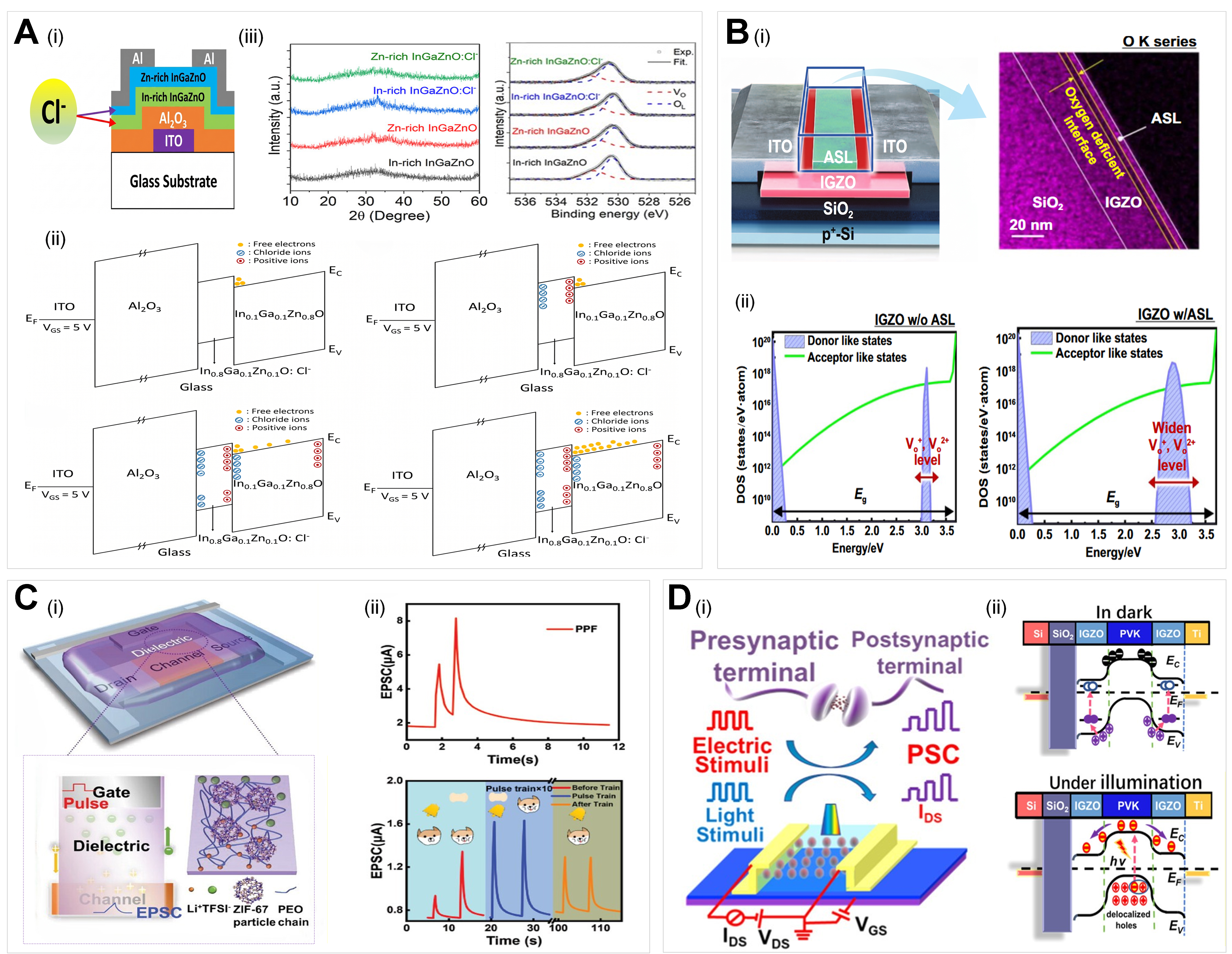
Figure 3. Materials engineering and microscopic mechanism regulation of a-IGZO synaptic transistors. (A) Channel atomic components: (i) Schematic illustration of the location-selective chloride (Cl-) modulation-doped IGZO dual-channel synaptic transistors. (ii) Energy band and ion distribution model during the potentiation process, elucidating the ion-regulated synaptic weight update mechanism. (iii) O 1s XPS spectra and XRD patterns of the channel regions, demonstrating the passivation and modulation of Vo levels via Cl-doping. Adapted from Ref.[57] under the CC BY 4.0 license. Copyright 2025, The Authors; (B) Back-channel engineering: (i) 3D schematic illustration of an IGZO phototransistor featuring an ASL at the back-channel, alongside the cross-sectional image and EDS mapping highlighting the oxygen-deficient interface. (ii) Proposed subgap DOS models for the IGZO phototransistors without and with the ASL, illustrating the widened subgap defect levels. Adapted from Ref.[62] under the CC BY 4.0 license. Copyright 2025, The Authors; (C) Molecular dynamics of dielectric: (i) Schematic of an individual EGT in a high-density artificial synapse array (100 × 100) with a lateral-gate structure, highlighting the ionic conduction framework enhanced by ZIF-67 porosity. (ii) Representative PPF and long-term EPSC responses, showing the enhanced synaptic performance. Adapted from Ref.[22] under the CC BY 4.0 license. Copyright 2023, The Authors; (D) Heterojunction bandgap engineering: (i) Schematic of emulating a biological synapse using an IGZO/CsPbBr3 NPs/IGZO TFT architecture under electrical and optical stimuli. (ii) Schematic energy-band diagrams of the IGZO/CsPbBr3 NPs/IGZO heterostructure in the dark and under illumination, illustrating photocarrier separation and transfer. Adapted with permission[76]. Copyright 2021, American Chemical Society. a-IGZO: Amorphous indium gallium zinc oxide; XPS: X-ray photoelectron spectroscopy; XRD: X-ray diffraction; ASL: aluminum sensitization layer; EDS: energy-dispersive X-ray spectroscopy; DOS: density of states; EGT: electrolyte-gated transistor; PPF: paired-pulse facilitation; EPSC: excitatory postsynaptic current; NPs: nanoparticles; TFT: thin-film transistor; ITO: indium tin oxide; PEO: poly(ethylene oxide); PVK: perovskite.