


Flexible circuits engineered for complex and extreme environments
 0
0 Abstract
Driven by the rising demand for mechanical adaptability, structural reconfigurability, and multifunctional integration, flexible circuits are gaining increasing importance in advanced electronic systems. They serve as key enablers for next-generation devices owing to their intrinsic mechanical compliance and stable electrical performance. In extreme environments, flexible circuits face severe reliability issues such as dielectric drift, interfacial delamination, crack propagation, and metal electromigration. Nevertheless, their deployment remains indispensable in aerospace systems operating under high temperature and pressure, in biomedical implants exposed to corrosive environments and dynamic loading, and in energy infrastructures subjected to strong acids, alkalis, and severe thermal gradients, since rigid alternatives cannot satisfy the stringent demands for mechanical adaptability and lightweight integration. This duality underscores both the challenges and the necessity of advancing flexible circuit technologies, where material innovations and cross-process strategies are crucial to ensure functionality under harsh conditions. This review provides a comprehensive account of the technological evolution of flexible circuit fabrication. On the materials front, the engineering of multiscale composite conductive networks has proven to significantly enhance interfacial bonding strength and environmental robustness. In terms of fabrication, subtractive manufacturing exhibits mature performance in patterning resolution, thermal effect suppression, and substrate compatibility. Additive manufacturing extends the frontier toward heterogeneous material integration and three-dimensional functional architectures. Meanwhile, conformal manufacturing provides novel paradigms for configurational control and interface modulation. By analyzing the characteristics and strengths of these fabrication strategies, this article further maps the application potential of flexible circuits in sensor arrays, communication modules, bioelectronic systems, and integrated photonics. It emphasizes the need to align process design with performance requirements. Key challenges remain, including reliability under extreme environments, delays in adopting sustainable manufacturing, and limited cross-process integration. Ultimately, the study argues that the future development of flexible circuits hinges on the innovation of functionalized materials, the establishment of sustainable fabrication platforms, and the convergence of hybrid manufacturing pathways. Together, these advances will drive a paradigm shift from passive structural flexibility to active system reconfiguration. Meanwhile, they will expand the scope of flexible electronics toward extreme, green, and reconfigurable application scenarios.
Keywords
INTRODUCTION
Flexible circuits, constructed upon pliable substrates, have evolved into high-performance electronic systems that demonstrate superior adaptability and engineering advantages across diverse application domains, far surpassing their rigid counterparts in versatility and integration[1,2]. In biomedical engineering, their inherent biocompatibility and mechanical flexibility have enabled widespread integration into implantable medical devices such as cardiac pacemakers and cochlear implants[3,4]. In aerospace applications, where systems must endure elevated temperatures and mechanical stress, flexible circuits have proven indispensable in cockpit display modules and satellite communication antennas, owing to their thermal resilience and systemic reliability[5]. Their lightweight structure and high integration density have also positioned them as foundational elements in wearable technologies, powering devices such as smartwatches and virtual reality (VR) headsets with enhanced form factors and functional sophistication[6,7]. Furthermore, their long-term operational stability and extended cycling lifespan have facilitated their adoption in automotive electronics and industrial control systems[8,9]. Despite significant progress, the deployment of flexible circuits in complex environments - marked by high temperature, humidity, mechanical load, and deformation - poses escalating demands on structural integrity and operational reliability. As applications extend beyond wearables to multifunctional systems under multi-stress conditions, developing fabrication strategies that concurrently ensure flexibility, integration, and robustness is essential for stable performance and future breakthroughs.
Since the inception of printed circuit technology in the 1930s, flexible circuits - defined by their mechanical pliability and high integration capability - have gradually emerged as a transformative class of electronic interconnects. In 1936, Austrian engineer Paul Eisler laid the foundation for printed circuit boards (PCBs) by pioneering the deposition of conductive patterns on insulating substrates. By the 1960s, the introduction of engineering-grade polymeric materials such as polyimide (PI) enabled a departure from rigid structures, marking the convergence of structural compliance and functional integration. Entering the 21st century, the application scope of flexible electronics has expanded from conformal two-dimensional (2D) surfaces to three-dimensional (3D)-wrapped architectures and stretchable devices, fueling their penetration into domains such as wearable electronics and smart displays[10,11]. Recent advances in flexible material systems include Samsung’s development of ultra-extensible PI films, ultrathin polarizers, and novel adhesives for foldable displays. These innovations enable substrates that are both thinner and stronger. Similarly, Beijing Oriental Electronics Co., Ltd. has leveraged its 6th-generation active-matrix organic light-emitting diode (AMOLED) production line and world-leading vapor deposition technology to produce ultra-flexible coverlay layers, allowing 0.03 mm-thick displays to bend and fold freely. In terms of advanced manufacturing, Huawei’s Pura X series employed low-temperature plasma etching to achieve nanoscale wiring on 0.03 mm-thick foldable screens without damaging the flexible substrate, improving interfacial compatibility and fracture resistance. In academia, Qingdao University of Technology, Zhejiang University, and Beihang University collaboratively developed an electric-field-driven multi-material microjet 3D printing technique to fabricate flexible nanosilver electrode array (FlexNEA) devices with a penetration success rate exceeding 99% and electrochemical impedance reaching 3.5 × 10⁴ Ω (1 kHz). Separately, Yang Huayong et al. at Zhejiang University pioneered a laser-induced carbonization with cryogenic transfer printing technique, enabling the fabrication of highly conductive architectures on 1.5 μm-thick hydrogels; by leveraging crack deflection and energy dissipation mechanisms, they elevated the stretchability of the conductive layer to five times its original limit, achieving 220% elongation after structural integration. Despite these breakthroughs, structural instability and functional degradation induced by multiscale stress concentration under high-density integration remain unresolved. Moreover, challenges persist at the system-integration level, including insufficient green manufacturing adoption and limited compatibility across hybrid fabrication routes - both of which constitute critical bottlenecks in achieving scalable, system-level flexible electronic architectures.
In the field of flexible electronics, “complex and extreme environments” refer to service conditions that far exceed conventional limits, characterized by the coupled action of multiple stresses. Representative cases include high mechanical loading, such as cyclic bending beyond 104 repetitions (TC183SC4); elevated temperatures, for instance, operating within a -55 to 150 °C range[12]; and high-humidity conditions, such as 93% relative humidity (RH) at 30 °C without condensation [as specified in the Joint Electron Device Engineering Council (JEDEC) standard JESD22-A101D.01]. These thresholds map directly onto application domains including aerospace structures, soft robotics, energy systems, and biomedical devices, where the long-term reliability of flexible circuits is severely challenged by dielectric drift, interfacial delamination, crack propagation, and metal electromigration. Overcoming these bottlenecks demands dual innovation in both materials and processing: on the materials side, the deployment of high-temperature-resistant substrates, low-permeability barrier coatings, and toughened composite adhesives; and on the processing side, the advancement of additive, subtractive, and conformal manufacturing, together with interfacial engineering.
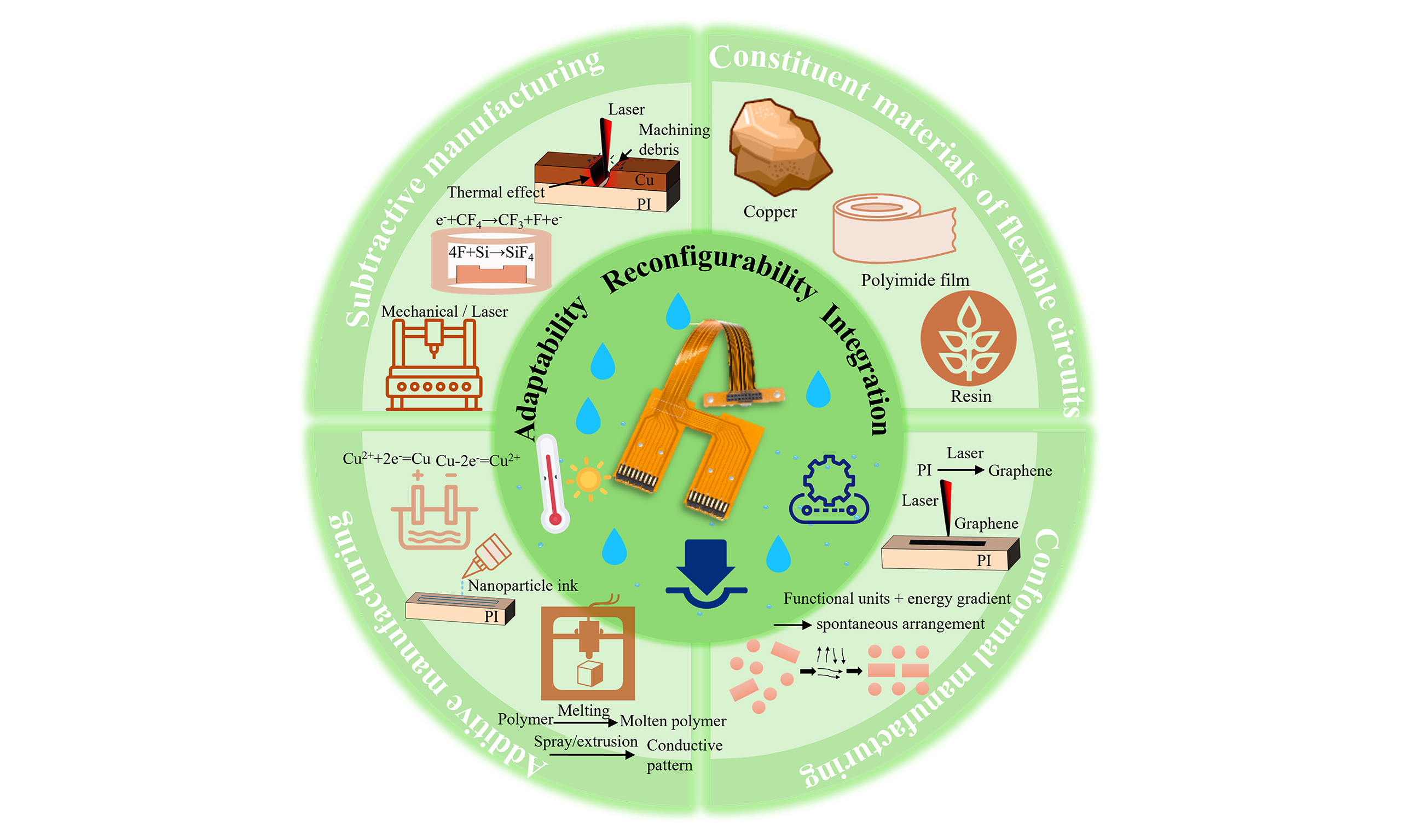
To address the aforementioned challenges, this review begins with a layer-by-layer analysis of coverlay materials, adhesives, conductors, base films, and stiffeners. It systematically evaluates their structural composition and functional characteristics, with a particular focus on how each layer balances electrical, physical, and mechanical performance under varying application conditions. The discussion then shifts to three primary fabrication paradigms - subtractive, additive, and conformal manufacturing - detailing their underlying construction principles and process workflows. By comparing these approaches in terms of patterning mechanisms, material compatibility, and scenario-specific adaptability, and by incorporating representative research advances, the review distills key technological trends and maps out the trajectory of future innovation. Figure 1 illustrates the functional attributes and representative applications of flexible electronic circuits. Core performance requirements - including biocompatibility, adaptability to extreme environments, bending resistance, and high-density integration - underpin their use in diverse scenarios. These functionalities enable flexible systems to offer high flexibility, enhanced reliability, extended operational lifespan, and lightweight form factors. Such characteristics highlight the pivotal role of flexible circuits in advancing next-generation biomedical devices, aerospace systems, industrial automation, and wearable electronics.
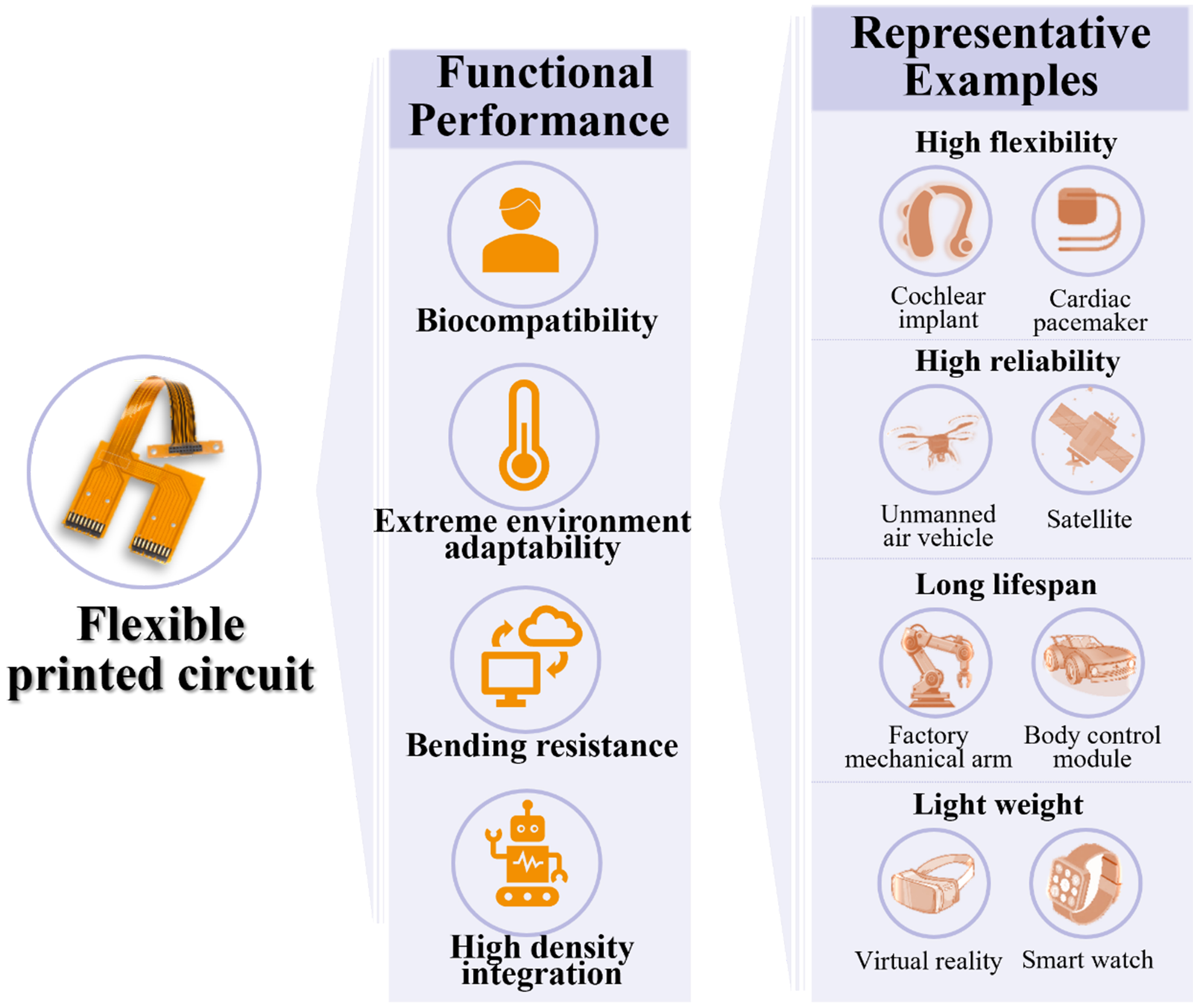
Figure 1. Advantages and representative applications of flexible circuits.
CONSTITUENT MATERIALS OF FLEXIBLE CIRCUITS
This chapter focuses on five critical material categories. It examines the synergistic roles these materials play in providing structural support, tailoring physical properties, and enhancing environmental adaptability. As illustrated in Figure 2, the hierarchical architecture and material configuration of flexible circuits are shown. The schematic depicts the multilayer structural elements - including coverlay, adhesive, base film, conductor, and stiffener - and illustrates the representative materials used for each category, highlighting their roles as foundational components in the overall system design.
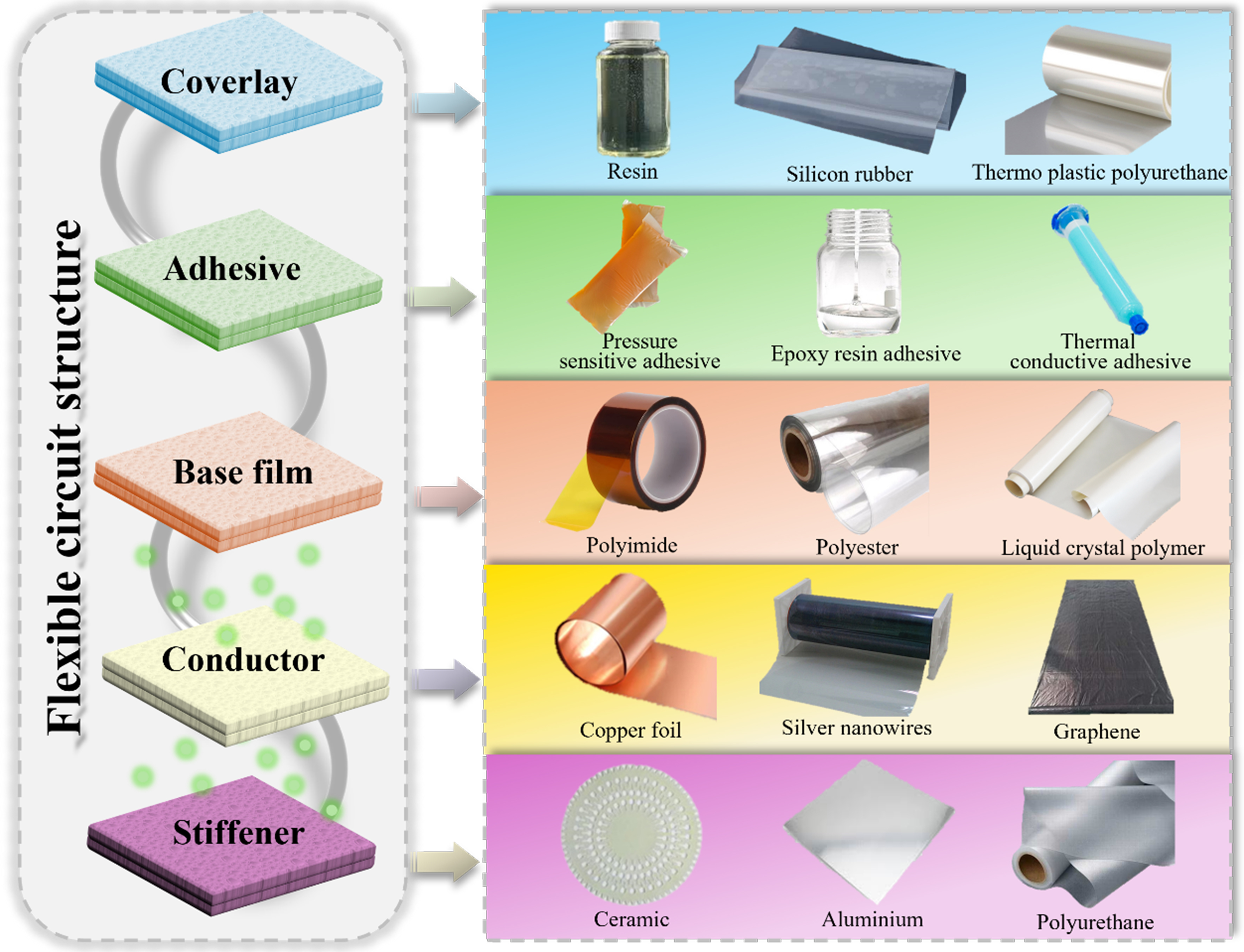
Figure 2. Layered structure and material components of flexible circuits.
The dielectric constant (εr) defines a material’s capacity to store energy under an electric field and is pivotal for ensuring signal integrity and reliability in insulating layers and substrates. Higher values increase capacitance and energy density but may induce dielectric loss and crosstalk, whereas lower values mitigate parasitic capacitance and delay, benefiting high-speed, low-power circuits. Under high mechanical loading, materials with stable dielectric responses and minimal drift are particularly advantageous. Thermal conductivity is particularly critical, as insufficient heat dissipation leads to local thermal accumulation, accelerating polymer chain scission and interfacial delamination under cyclic loading, which ultimately shortens device longevity. In parallel, dielectric properties are equally vital for long-term performance, since a stable dielectric constant across temperature and humidity ranges prevents signal leakage and capacitive drift, thereby extending the operational lifetime of devices. Equally important, the water vapor transmission rate (WVTR) directly affects environmental adaptability, since high WVTR enables moisture ingress that compromises insulation, corrodes conductors, and degrades encapsulant integrity, all of which cumulatively undermine service reliability and lifespan.
Base film material selection and research progress
As the foundational structural layer in flexible electronics, base film materials play a decisive role in determining the mechanical compliance, thermal stability, and environmental resilience of flexible circuits. As illustrated in Figure 3, the evolution of substrate materials for flexible circuits can be traced through a series of milestones. Each reflects advances in material performance that have progressively shaped the development of flexible electronics. In the 1960s, DuPont’s commercial launch of the Kapton® PI film marked a foundational milestone, providing exceptional thermal stability above 400 °C, a dielectric constant of 4.0 at 103 Hz, and strong chemical inertness. Such a dielectric constant is well suited for substrate layers in multilayer circuits, where sufficient insulation must be ensured without compromising mechanical robustness, establishing PI as the dominant substrate in early high-end flexible circuit systems[13,14]. However, as flexible electronics shifted toward low-cost, rapid-fabrication, and multi-environment applications, the high patterning difficulty and processing cost of PI began to hinder its scalability[15]. Since the 1970s, polyester base film - particularly polyethylene terephthalate (PET) - has attracted significant interest due to its low cost and ease of processing[16]. PET, in particular, has demonstrated promising performance in flexible displays and sensor platforms owing to its flexibility and thermal stability at low temperatures[17]. Nevertheless, conventional PET suffers from limited heat resistance (< 80 °C) and modest mechanical strength (yield strength < 80 MPa), restricting its use under high-temperature and high-stress conditions. In the late 1980s, materials such as polyamide (PA) and polyurethane (PU) gained traction in 3D deformable circuit systems due to their superior ductility and chemical resistance[18]. Entering the 1990s, the rise of wireless communication and millimeter-wave radar applications spurred interest in liquid crystal polymers (LCP), with dielectric constants of 2.9-3.0 and a loss tangent below 0.002. These low values are advantageous in high-frequency signal layers, as they minimize propagation delay and crosstalk, thereby supporting efficient transmission in antennas and microwave interconnects, and outstanding interfacial stability, rendering them prime candidates for high-frequency antennas and microwave transmission lines[19,20].
Figure 3. Development timeline and technological progress of flexible circuit base film. PI: Polyimide; PET: polyethylene terephthalate; PA: polyamide; PU: polyurethane; LCP: liquid crystal polymers; PAIU: poly(amide-imide-urethane).
In the 21st century, the development of flexible circuit base film has entered a new phase characterized by the dual pursuit of composite functionality and environmental sustainability. To meet the simultaneous demands for thermal stability and mechanical extensibility, poly(amide-imide-urethane) (PAIU) copolymers have been introduced into flexible electronics. These materials leverage a thermally resistant amide-imide backbone in combination with PU side chains that impart elasticity, enabling excellent mechanical stability under high-folding and high-strain conditions. PAIU-based systems have demonstrated superior dynamic mechanical behavior, including elongation rates exceeding 200%, thereby significantly enhancing the mechanical reliability of flexible devices[21]. Concurrently, growing global emphasis on sustainable electronics and e-waste mitigation has driven the emergence of recyclable and degradable substrate materials. A joint research effort by the Massachusetts Institute of Technology (MIT) and the University of Utah has yielded a photopatternable, degradable polyimide network that supports conventional lithographic processes while maintaining desirable physical and electrical properties[22]. This material not only streamlines fabrication through photopatterning but also facilitates the separation of electronic components and precious metals under mild conditions, offering a closed-loop approach to sustainable device fabrication and end-of-life recovery. Recently, the same MIT-Utah-Meta collaborative team further advanced this concept by developing a degradable photo-crosslinked polyimide mesh substrate. This substrate simultaneously achieves excellent thermal conductivity (0.37-0.54 W·m-1·K-1), robust dielectric performance [dielectric constant (Dk) = 2.81-3.05, dielectric loss (Df) < 0.024], and reliable mechanical strength (Young’s modulus ~50 MPa, elongation > 5%). Its architecture incorporates reversible ester linkages, enabling controllable depolymerization and efficient component disassembly - thereby reconciling the trade-off between high performance and material recyclability in next-generation flexible electronics.
Resilience under extreme environments has become a critical benchmark[23]. At the device scale, thermal loads induce interfacial stress accumulation, accelerating degradation and compromising structural integrity. These findings highlight a paradigm shift toward multidimensional robustness. Future progress hinges on developing material platforms that couple extreme-environment tolerance, long-term reliability, and recyclability - key to enabling durable, high-integration, and eco-conscious next-generation electronics.
Conductive material selection and research progress
As the central determinant of signal integrity and electrical performance, conductive materials serve as a core driver of innovation in flexible circuits, embodying the deep convergence of materials science and fabrication technology. As illustrated in Figure 4, the evolution of conductive materials for flexible circuits has progressed through distinct stages. These milestones illustrate how successive material innovations have driven advances in circuit performance and application scope. In the 1970s, copper emerged as the dominant conductor for early flexible circuits due to its high electrical conductivity (~5.8 × 10⁷ S/m) and respectable mechanical strength (yield strength ~60 MPa). However, its high density (8.96 g/cm3) and intrinsic rigidity led to rapid fatigue accumulation and increased failure risks under repeated bending or dynamic deformation, limiting its long-term viability in next-generation flexible systems[24]. To address the demands of stretchable and deformable applications, research has increasingly focused on intrinsically flexible conductive polymers such as polyaniline (PANI) and polypyrrole (PPy). These materials offer native compliance and tunable conductivity via molecular engineering or dopant modification. For example, PANI conductors fabricated via inkjet or screen printing effectively simplify the wiring process while reducing processing temperature and energy consumption. Nonetheless, such polymeric conductors typically suffer from poor environmental stability; conductivity degradation exceeding 50% has been reported under humid conditions, posing a significant limitation to their long-term operational reliability[25].
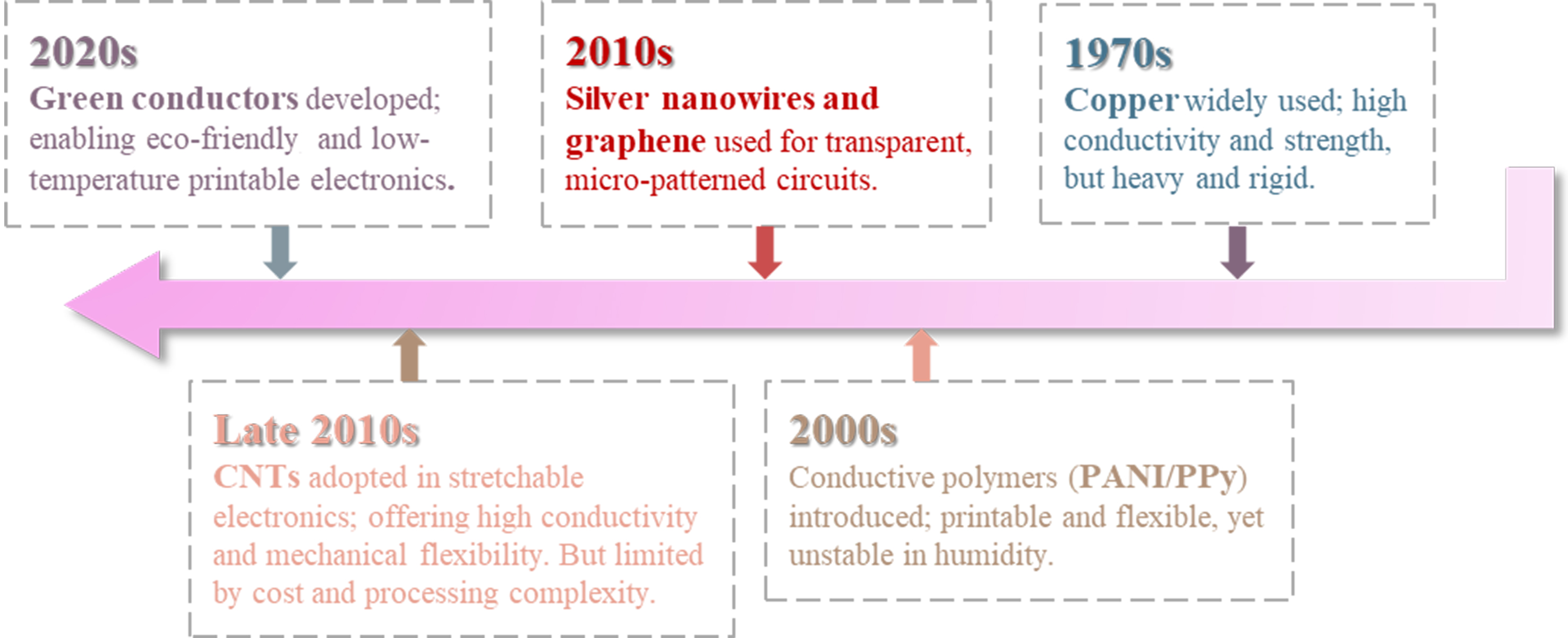
Figure 4. Development pathway and material transition of conductive components in flexible circuits. CNTs: Carbon nanotubes; PANI: polyaniline; PPy: polypyrrole.
In the 21st century, the integration of nanomaterials has catalyzed a substantial leap in the performance landscape of flexible conductive materials. Among them, silver nanowires (AgNWs) have emerged as a key enabler for transparent and flexible electrodes, owing to their low sheet resistance and high optical transmittance (> 90%), and are widely deployed in wearable displays and transparent touch interfaces[26]. However, AgNWs are inherently sensitive to oxygen and humidity, often exhibiting rapid electrical degradation. To address this, graphene encapsulation and surface passivation strategies have been developed, significantly enhancing the environmental stability and operational lifetime of AgNW-based devices[27]. Carbon-based nanomaterials such as graphene and carbon nanotubes (CNTs) have further expanded the physical boundaries of flexible conductors. Graphene, with its single-layer hexagonal lattice, offers exceptionally high theoretical conductivity and optical transmittance (~97.7%), and has been successfully micropatterned on flexible base film using femtosecond laser techniques. To overcome the challenges in interlayer aggregation and dispersion uniformity, approaches involving chemical functionalization and intercalants have been employed to improve its compatibility and homogeneity in composite systems[28]. CNTs combine outstanding conductivity (~108 S/m) with remarkable tensile strength (~80 GPa), making them suitable for highly deformable environments. Current mainstream fabrication techniques, such as low-temperature solution deposition, have enabled the continuous roll-to-roll production of CNT-based flexible films[29]. Nevertheless, challenges related to high synthesis cost and uniformity control remain major obstacles to large-scale deployment, prompting parallel efforts in cost-effective synthesis, interfacial engineering, and multi-material hybridization[30]. Entering the 2020s, sustainability has emerged as a strategic priority in conductor material research. Nanocellulose, as a renewable, biodegradable, and biocompatible natural polymer, has attracted increasing interest as a candidate for green conductive materials. By integrating graphene, silver nanoparticles, or CNTs into the nanocellulose matrix, composite conductive networks have been developed that exhibit flexibility, conductivity, and environmental friendliness. These systems have demonstrated compatibility with low-temperature wet processing and 3D printing, and are promising for wearable sensing, implantable diagnostics, and recyclable electronics[31]. Although their overall performance still lags behind traditional inorganic materials, their scalability and strategic relevance within green manufacturing frameworks are becoming increasingly prominent.
In summary, flexible conductive materials are evolving from metal-centric designs to multifunctional systems that integrate polymers, carbon nanomaterials, and bio-derived composites. This shift enables concurrent improvements in conductivity, flexibility, and environmental resilience - supporting scalable deployment in healthcare, wearables, and the Internet of Things (IoT). However, current architectures face critical limitations: unstable heterogeneous interfaces, resistance drift, and delamination under thermal-mechanical-humidity stress. Addressing these challenges requires a transition from conductivity-driven design to resilience-oriented strategies that emphasize interfacial stability, multi-field coupling, and long-term durability. Equally important is the development of recyclable and biodegradable conductors to align flexible electronics with sustainability goals. Together, these advances will accelerate the transition from discrete devices to integrated, intelligent, and eco-compatible electronic systems.
Coverlay materials, adhesives, and stiffeners: selection and research progress
As the primary protective barrier in flexible devices, the thermal, mechanical, and dielectric properties of coverlay materials directly dictate their service lifespan and environmental adaptability. Traditional epoxy resins, while offering excellent electrical insulation (volume resistivity ~1013-1016 Ω·m) and mechanical strength, are prone to degradation under extreme environmental conditions, compromising coverlay integrity and ultimately shortening device longevity[32]. Similarly, silicone rubber has been adopted in packaging due to its compliance, though its dielectric constant (> 2.7) and thermal conductivity restrict its role. Although such materials can buffer mechanical strain, their relatively high WVTR makes them less suitable for harsh or humid environments, further limiting lifespan. To address these limitations, researchers have developed multiscale filler composite strategies aimed at synergistically enhancing thermal and mechanical performance. For instance, Zhang et al. introduced spherical alumina (S-Al2O3) and graphene nanoplatelets (GnPs) into silicone rubber matrices to construct hierarchical thermal conduction networks[33]. This approach raised the thermal conductivity to 3.37 W/m·K while maintaining a low density (~2.62 g/cm3), demonstrating a promising balance between weight and heat dissipation. Meanwhile, the hierarchical network reduced free-volume channels, lowering WVTR and thereby improving environmental stability. Building upon this, Jiang et al. extended the composite design to additive manufacturing by developing a 3D-printable polylactic acid (PLA) matrix incorporating 70 wt% alumina and 1 wt% graphene[34]. The resulting composite achieved a thermal conductivity of 2.4 W/m·K, effectively bridging the gap between thermal performance and structural processability for complex 3D interconnects.
Conventional epoxy-based adhesives, despite their favorable bonding strength and compatibility with existing fabrication processes, generally exhibit low thermal conductivity (< 0.3 W/m·K) and are prone to fatigue failure under sustained dynamic loading. In response, recent research has shifted toward the development of next-generation adhesive systems that combine high electrical and thermal conductivity with reconfigurability. Among these, conductive composite adhesives filled with silver nanoparticles have demonstrated substantial performance enhancements. By forming continuous conductive networks, these systems significantly reduce interfacial resistivity (as low as 4.2 × 10⁻³ Ω·g·cm-2)[35]. More importantly, the incorporation of thermoreversible molecular networks imparts these adhesives with self-healing and reconfigurable capabilities under thermal stimuli. This not only expands the processing window during device fabrication but also provides a promising material foundation for repairable and reusable flexible electronic systems.
As a critical component for maintaining mechanical integrity, stiffener structures play a key role in resisting multiaxial deformation, suppressing structural instabilities, and prolonging device service life. Conventional reinforcement films based on PI and PET, despite their favorable flexibility, are prone to microcracking under high-frequency cyclic strain (> 103-105 cycles), which can lead to conductive path failure. Moreover, their relatively high coefficients of thermal expansion tend to induce interfacial thermal stress concentration in multilayer or thermally processed systems, accelerating material fatigue[36]. To overcome these limitations, various stretchable reinforcement structures have been developed. Characterized by porous networks and high extensibility, these materials can sustain strains over 30% while maintaining fatigue lifespans exceeding 10,000 cycles, showing excellent adaptability in flexible sensing and wearable applications[37]. Furthermore, dynamic covalent-bond-based reinforcement materials have been introduced into flexible systems. For example, Ying et al. proposed a biomimetic PU elastomer inspired by muscle architecture, which utilizes a dynamic hydrogen-bonding network to achieve 1,900% elongation at break and a toughness of
Key materials for flexible circuits, their properties, challenges, solutions, and typical applications
| Wiring material | Material system | Thermal conductivity (W/m·K) | Dielectric constant | Electrical conductivity (S/m) | Young’s modulus (Gpa) | Under extreme environments | Typical applications | |
| Challenges | Solutions | |||||||
| Base film | PI | 0.15-0.3 | 3-4 | 10-16-10-14 | 3-4 | Dielectric drift; chains | Fluorination; fillers | Conventional substrates |
| PET | 0.15-0.24 | ~3.7 | 10-16-10-13 | 2.2 | Poor thermostability | Crosslinking; blending | Displays and sensors | |
| LCP | 0.2-0.4 | 2.9-3.0 | 10-12-10-10 | 0.1-0.5 | Interfacial delamination | Adhesion promotion | High-frequency antennas | |
| PAIU | ~0.26 | 3.0-3.8 | 10-17-10-16 | 4.0-8.3 | Poor oxidation resistance | Antioxidant additives | high-stress applications | |
| Photo-curable PI | 0.37-0.54 | 2.81-3.05 | - | 0.05 | Moisture sensitivity | Passivation coatings | biodegradable electronics | |
| Conductive | Cu | 400 | ~1 | ~5.8 × 10⁷ | 110-130 | Electromigration | Protective coating | Conventional metallic layers |
| PANI | ~0.1 | ~2 | 10-10-10-5 | 1-4 | UV/moisture degradation | Graphene-based composites | Flexible sensors | |
| AgNWs | ~429 | - | 107-10-8 | ~85 | Junction instability | ALD encapsulation | Transparent electrodes | |
| Graphene | 2,000-5,300 | 2.5-4.5 | 106-108 | 783-908 | Wrinkling deformation | Multilayer stacking | Transparent conductive films | |
| Nanocellulose | 0.5-1.585 | - | 1.6 × 10⁻⁴ | 50-160 | Moisture swelling | Hydrophobic modification | Bioelectronic devices | |
| Coverlay | Epoxy resin | ~0.2 | 2.5-5.5 | ~10-14 | 0.2-3 | High WVTR | Hybrid composite barriers | General coverlay |
| Silicone rubber | 3.37 | 2.7-3.3 | 0.1-1,000 | ~0.0015 | Conductivity dilemma | Hierarchical fillers | High-frequency circuits | |
| TPU | 0.15-0.25 | ~3.6 | - | 4 | Moisture swelling | Crosslinking | Integrated coverlay | |
| Adhesive | Epoxy adhesive | 0.1-0.2 | 3-4.7 | 10-14-10-17 | 2-6 | High WVTR | Nanofillers | Wearables |
| UV-curable | ~0.2 | 2-4 | - | ~1 | Brittleness | Flexible monomers | Sensors | |
| Stiffeners | Ceramic | 26-30 | 2-10 | 10-14-103 | ~300 | Poor flexibility adaptation | Thinning | Flexible displays |
| FR-4 substrate | 0.25-0.35 | 4.2-4.8 | 10-14-10-16 | 14-24 | Brittleness | Composite design | Power modules | |
However, key challenges remain. A fundamental trade-off persists between thermal conductivity and stretchability, as most thermally conductive polymers exhibit elongation below 50%, limiting their use in deformable and long-life devices. Heterogeneous interfaces remain prone to delamination (20%-30%) under extreme environments, undermining reliability. Additionally, less than 25% of materials used are recyclable or biodegradable, slowing the shift toward sustainable electronics. To overcome these limitations, material research is advancing toward intelligent, adaptive, and eco-conscious systems. Hybrid phase-change composites - such as paraffin/multilayer graphene hybrids - and conductive liquid crystalline polymers are emerging as solutions that balance thermal conductivity with mechanical compliance[39]. Dynamic bonding networks and microstructured dissipative layers are being deployed to stabilize interfaces under thermal cycling. On the sustainability front, bio-based materials such as PLA and nanocellulose are achieving improved strength and reliability[31], laying the groundwork for degradable electronics. Accordingly, future research should prioritize integrated strategies that tune thermal, dielectric, and barrier properties in concert. It is the synergistic balance among these parameters - rather than the pursuit of any single attribute - that will determine service lifespan and ensure environmental adaptability in next-generation flexible electronic systems. Ultimately, the convergence of cross-disciplinary technologies will drive materials innovation from structural reliability toward integrated, intelligent, and sustainable electronics.
The reliability of flexible devices, a decisive criterion for their engineering viability, is fundamentally governed by the interplay of material systems and fabrication processes. Substrate films underpin structural stability and mechanical compliance; PI and LCP, for example, sustain interfacial integrity under elevated temperatures and cyclic bending, thereby reducing risks of delamination and dielectric drift. Conductive layers define electrical fidelity, yet entail inherent trade-offs: copper ensures high conductivity but suffers from strain-induced cracking, whereas AgNWs, graphene, and CNTs provide superior deformability but remain vulnerable to environmental degradation. Coverlays and adhesives, through their dielectric constant and WVTR, dictate insulation reliability, as excessive WVTR accelerates metal corrosion and local leakage, while stiffener layers suppress structural instability and delay fatigue through stress redistribution, with their thermal conductivity and dielectric stability exerting critical influence on long-term durability. In practice, device reliability emerges as the collective outcome of multiscale and multiphysics couplings: localized stresses during repeated deformation propagate interfacial cracks and conductor fatigue; moisture penetration and thermal cycling trigger polymer relaxation and accelerate electrical decay; and dielectric fluctuations under high-frequency operation induce impedance drift and signal attenuation. These degradation pathways converge into characteristic failure modes, including delamination, warpage, electrochemical corrosion, and loss of electrical continuity. Addressing these challenges demands integrated reliability frameworks that extend beyond single-material optimization. Predictive modeling via finite element analysis and digital twins enables proactive identification of thermo-electro-mechanical interactions, guiding optimized structural layouts and interlayer matching. Process-level innovations such as self-assembled monolayers, plasma activation, and atomic layer deposition passivation strengthen interfacial adhesion and stability, while self-healing networks based on dynamic covalent or hydrogen bonding mitigate microcracks at their inception, thereby prolonging operational lifetimes.
Looking forward, two imperatives define the research trajectory: advancing adaptability to extreme environments and establishing standardized reliability protocols. In aerospace, implantable biomedical systems, and high-frequency communications, devices must sustain performance under radiation, humidity, elevated temperatures, and complex loading, necessitating materials capable of enduring multiphysics extremes over prolonged operation. Concurrently, the absence of harmonized testing standards remains a critical bottleneck, as current bending, fatigue, and hygrothermal protocols lack cross-platform comparability, undermining industrial translation. Developing unified protocols that codify strain modes, cycling frequencies, and failure thresholds will be pivotal to accelerate the maturation of flexible electronics from laboratory prototypes to scalable, durable, and application-ready technologies.
WIRING TECHNIQUES FOR FLEXIBLE CIRCUITS
Subtractive manufacturing
Subtractive manufacturing, rooted in rigid PCB production, remains a foundational strategy for flexible circuits by selectively removing conductive layers such as copper foil to define high-precision interconnects. Its inherent advantages - high resolution, equipment compatibility, and low cost - have enabled widespread adaptation to flexible substrates. With advances in etching and mechanical/laser-based cutting, subtractive methods now offer micron-level control across diverse substrates, supporting scalable applications in flexible displays, wearables, and biosensors. As a result, subtractive manufacturing continues to dominate large-area flexible electronics fabrication, forming a technological continuum from traditional processes to high-precision laser systems.
Cutting techniques
Mechanical cutting techniques
In flexible circuit fabrication, mechanical cutting refers to a subtractive technique in which concentrated mechanical forces - such as compression, shearing, or blade motion - are applied to separate materials and generate desired circuit geometries. This principle ensures structural shaping by inducing localized stress concentration, deformation, and eventual fracture along the tool path. Mechanical cutting remains a foundational processing approach due to its high throughput, low cost, and broad equipment compatibility. Among its typical variants, stamping and blade cutting serve as representative techniques tailored to different production needs. Stamping operates by pressing a metallic mold against the workpiece with high pressure, generating shear stresses that exceed the material’s fracture strength. Stamping leverages metallic molds and high-pressure systems, applying instantaneous compressive forces to induce material deformation or fracture, offering exceptional repeatability and processing speed - making it ideally suited for standardized, large-scale manufacturing workflows[40]. In contrast, blade cutting provides greater flexibility for diverse and low-volume production scenarios. Here, the sharp tool edge slides or presses against the substrate, with relative motion producing precise shearing and material separation. It achieves positioning accuracies within ±0.15 mm, with high-precision systems capable of maintaining repeatability down to ±0.01 mm[41]. Cutting speeds typically range from 200 to 2,300 mm/s, adequately meeting the demands of rapid patterning for circuits with low to moderate complexity. However, the resolution of mechanical cutting remains constrained by tool size and material mechanical response.
As illustrated in Figure 5, cutting technologies in flexible circuits encompass a wide range of materials and application scenarios, demonstrating high-precision patterning capabilities and broad adaptability to wearable and deformable electronics. In 2006, Ke-Wang et al. conducted a systematic investigation into the edge morphology evolution and the influence of die parameters on cutting quality during the blanking process of flexible printed circuits (FPCs)[46]. By employing 300× optical microscopy to characterize the FPC cross-section, four distinct zones induced by shear stress were identified: rollover region, smooth shear zone, fracture surface, and burr formation area. The study revealed that for single-layer structures - where the copper foil is laminated only on one side and the total thickness is relatively low - smaller die clearances (e.g., 0.02 mm) facilitate cleaner edges due to enhanced stress concentration and precise shearing. In contrast, for double-sided structures with increased thickness and stiffness, larger clearances (e.g., 0.03 mm) effectively alleviate interlayer shear stress accumulation, thereby improving interface integrity and edge quality. These findings offer valuable theoretical guidance and process parameters for controlling interface stability in flexible device cutting.
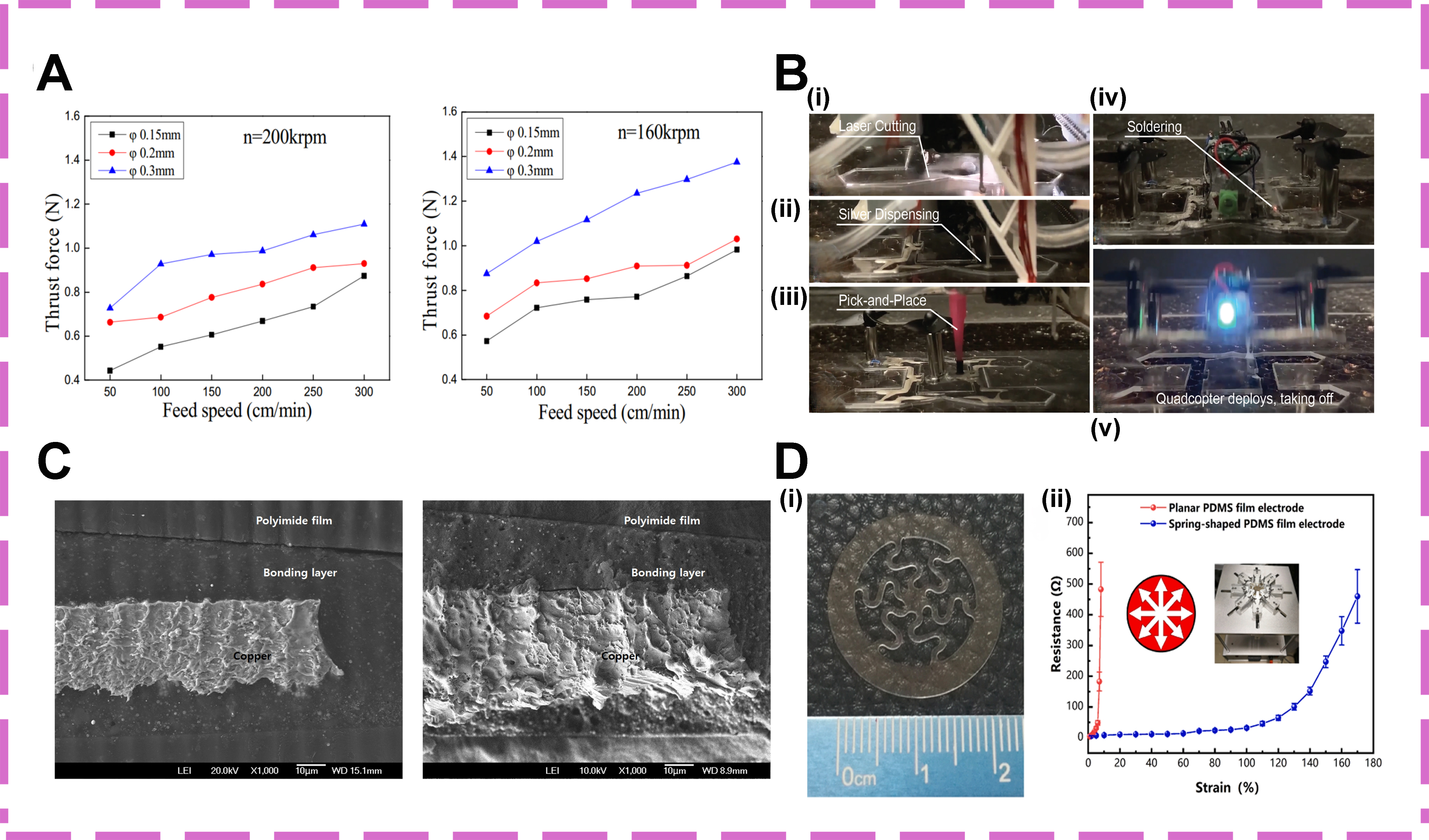
Figure 5. Cutting techniques for fabrication and performance characterization of flexible electronic circuits. (A) Relationship among feed speed, drill diameter and thrust force[42]; (B) Making a Device with LaserFactory[43]; (C) SEM images of cross-sectional view: under air cutting and under solvent cutting[44]; (D) (i) Picture of spring-shaped PDMS film cutting by UV nanosecond laser, (ii) Resistance-strain curves of different PDMS film electrodes[45]. SEM: Scanning electron microscopy; PDMS: polydimethylsiloxane; UV: ultraviolet.
Nevertheless, the productivity and repeatability advantages of stamping are offset by its rigidity, making it less suited for fine or multilayer structures. This limitation highlights the transition toward alternative approaches such as blade-based cutting. However, traditional mechanical cutting still faces several inherent challenges. At the microscale, high-speed cutting often induces localized heat accumulation, leading to thermal softening of materials, dimensional drift, and edge collapse[47]. Additionally, mechanical loading can introduce burrs and concentrated stress zones, further constraining the applicability of this technique in high-resolution patterning. These drawbacks have driven increasing attention toward tool-based cutting strategies, which, while more adaptable, bring their own set of challenges that must be systematically addressed. As summarized in Table 2, stamping and mechanical cutting each offer distinct advantages across forming mechanisms, processing precision, production efficiency, and application adaptability.
Comparative analysis of stamping and cutting techniques
| Characteristic | Stamping technology | Cutting technology |
| Mechanism | High-pressure shear using metallic dies | Relies on tool-material movement |
| Precision | ~0.05 mm (determined by die quality and clearance) | ~0.15 mm; repeatability up to ±0.01 mm, but limited by tool wear and material response |
| Efficiency | A few tenths of a second per sheet; highly suited for large-scale production | Tens of seconds per sheet; suited for small- to medium-volume use |
| Production cost | High initial die cost; very low unit cost in mass production | Low upfront cost (no dies required); relatively higher unit cost |
| Material | Commonly uses PI and PET | Also uses PI and PET adaptability |
| Applications | Standardized, high-volume production | Prototyping and customized devices |
| Challenges | Limited adaptability; sensitive to die wear and clearance | Tool wear, thermal effects, burr formation |
| Advances | High-precision dies and advanced ceramic composite molds improve durability and edge quality | Intelligent path planning and closed-loop control enhance precision and adaptability |
In 2012, Zhang et al. systematically investigated the influence of spindle speed (120-200 krpm), feed rate (50-300 cm/min), and drill diameter (0.15/0.20/0.30 mm) on cutting force during micro-drilling[42]. Using a DYTRAN 1051 micro-force sensor (sampling rate: 5,000 Hz), they recorded real-time thrust variations, revealing that distinct material-dependent cutting responses-maximum force occurred in the copper foil layer, followed by the adhesive layer, with the PI layer exhibiting the lowest resistance. Thrust force consistently increased with larger drill diameters and higher feed rates, whereas elevated spindle speeds effectively suppressed force growth [Figure 5A]. High spindle speed and low feed rate were shown to effectively mitigate local stress concentration and deformation, enhancing hole-position stability, which is crucial for preserving FPC structural integrity under complex loading environments. In 2016, Zheng et al. compared micro-drilling tool wear behavior in flexible FPCs vs. rigid PCBs[48]. They found that tool degradation was strongly influenced by feed rate and drilling repetition. As the number of holes increased from 0 to 500, the process capability index (CPK) dropped significantly; the PI burr thickness increased from 20 to 45 μm, and burr height rose from 10 to 14 μm-clearly degrading hole quality. Increasing spindle speed to 158 krpm partially alleviated wear progression and improved hole-wall morphology.
Stamping capitalizes on metallic dies and high-pressure shear to achieve rapid and precise material separation, offering excellent repeatability and high throughput, making it indispensable for standardized, large-scale workflows. However, its reliance on rigid die geometries limits adaptability; in multilayer FPCs, improper die clearance exacerbates interfacial stress accumulation, leading to delamination, burr formation, and compromised edge quality. Blade cutting, by contrast, demonstrates greater adaptability across diverse designs and low-to-medium production volumes. With achievable positioning accuracies down to
Recent advancements in boron nitride ceramic matrix composite (BN-CMC) molds combined with thermoforming have significantly improved cutting efficiency and surface finish, exemplifying the “processing-structure-property” coupling in flexible circuit fabrication[49]. Meanwhile, the integration of intelligent control and perception algorithms is fostering a shift toward digitalized, closed-loop machining systems[50]. Mechanical cutting is thus evolving into a triadic paradigm that unifies material innovation, process optimization, and adaptive control - supporting macro-to-micro scale patterning. Under artificial intelligence (AI) and data-driven guidance, toolpath planning, stress prediction, and deviation correction are becoming increasingly precise, mitigating multiscale stress concentration, warpage, and delamination. Concurrently, green manufacturing initiatives are promoting low-toxicity lubricants and energy-efficient workflows.
Laser cutting techniques
Since its inception, laser cutting technology has played a pivotal role in the electronics industry due to its non-contact processing nature, high precision, and broad material adaptability. Unlike conventional mechanical methods, laser cutting eliminates the need for physical tool interaction, enabling efficient fabrication of intricate geometries, through-holes, and multilayer windows in flexible circuits. The technology originated in the 1960s. CO2 lasers, with their strong absorption in non-metallic substrates, were widely used in early non-metal applications. However, their long wavelengths lead to deep energy penetration and large heat-affected zones, often resulting in thermal damage such as surface carbonization, melting[51]. In contrast, neodymium-doped yttrium aluminum garnet (Nd:YAG) lasers, with shorter wavelengths, offered improved precision for thin metallic films but still suffered from excessive thermal diffusion in polymer substrates, restricting their applicability. Entering the 21st century, femtosecond lasers emerged as a disruptive solution due to their ultrashort pulse duration and extremely high peak power, achieving so-called “cold cutting” that significantly suppresses thermal effects. This made them ideal for edge definition in thermally sensitive and multilayered flexible materials, where conventional techniques fall short[52]. Additionally, ultraviolet (UV) lasers - particularly those with 355 nm wavelength - have expanded the resolution frontier in flexible circuit cutting[53]. These UV nanosecond lasers have demonstrated exceptional performance in layer-specific patterning, microvia drilling, and surface cleaning, with typical cutting speeds around 20 mm/s, kerf widths near 55 μm[54], and heat-affected zones controlled to ~2.3 μm[45]. Overall, laser cutting systems now routinely achieve 10 μm-scale resolution for flexible substrates ranging from 5 to
Performance comparison of typical laser types in flexible electronics processing
| Property | CO2 Laser | Nd Laser | Fs Laser | Fs UV Laser |
| Wavelength | 10.6 µm | 1.064 µm | 800 nm | 355 nm |
| Accuracy | ~20 μm | ~10 μm | ~5 μm | < 5 μm |
| Thermal effect | ~10 μm | ~2.3 μm | ~1 μm | < 1 μm |
| Materials | Mainly for non-metals | Conventional polymer and metal composites | Ultrathin metals and polymer materials | Heat-sensitive and specialized materials |
| Cost | Low | Moderate | High | Medium high |
| Speed | Relatively fast | Fast | Slow | Slow |
| Technical limitations | Significant thermal damage, limited accuracy | Heat diffusion material restrictions | High-cost complex equipment | Small spot size requires precise control |
As early as 2006, Huske et al. employed UV nanosecond lasers with ~20 μm focused spot sizes to achieve high-fidelity patterning of FPCs[56]. By carefully modulating single-pulse energy and implementing multipass scanning strategies, the process preserved cut continuity while effectively mitigating carbonization and recasting in the heat-affected zone. The resulting cut edges exhibited negligible mechanical stress concentration and residue accumulation, with the copper-polyimide interface remaining structurally intact - substantially reducing the risk of warpage, delamination, and fatigue-induced failure. Advancing this paradigm, in 2021, Nisser et al. proposed an integrated electromechanical assembly system[43]. Anchored on a standard CO2 laser platform, the system retained precise cutting capabilities while integrating a silver paste nozzle and lightweight robotic arm, maximizing spatial efficiency. It supported circuit fabrication, with a minimum line width of 0.75 mm, enabled high-precision manipulation of components up to 65 g, and achieved rapid soldering and ink curing via localized laser heating. This approach reduced silver ink curing time from two hours to just five minutes, lowering overall system cost to approximately $150 and significantly enhancing throughput and integration - thus offering a scalable solution for low-cost, application-specific flexible electronics. The process chain integrated laser cutting, silver dispensing, pick-and-place, and soldering into a unified workflow, ultimately culminating in the successful demonstration of a functional device [Figure 5B]. In 2013, Kim et al. introduced an innovative method for laser cutting FPCs in liquid media, where coolant-assisted ablation effectively reduced carbon residue and HAZ propagation[44]. Experiments showed that the transmittance of 355 nm UV laser in water was 27.7%, necessitating a power increase from 2-10 W (in air) to 4-18 W to maintain a target energy density of 15.7-235.7 J/cm2. Thermal simulations revealed a 100 K temperature drop in the copper layer within 3 ms and an 11% reduction in HAZ width. Scanning electron microscopy (SEM) cross-sectional images further confirmed that solvent-assisted cutting produced cleaner interfaces and significantly narrowed the bonding-layer damage compared with conventional air cutting [Figure 5C]. In 2022, Wu et al. proposed a “heat generation-diffusion co-regulation” strategy for minimizing thermal damage during UV laser cutting of polydimethylsiloxane (PDMS) films[45]. By reducing laser fluence (1 W, 1,300 mm/s,
Despite these advances, two major obstacles remain. First, the high cost and operational complexity of femtosecond and deep-UV systems limit industrial scalability. Second, thermal control during ultrathin substrate machining remains challenging, often causing edge carbonization, warping, or delamination in multilayer structures due to stress transmission. To overcome these challenges, research is focusing on multidimensional parameter tuning and intelligent feedback control. Techniques such as dual-pulse modulation, segmented energy delivery, and real-time thermal compensation have established stress-aware machining frameworks that improve yield and adaptability. Looking ahead, laser cutting is expected to evolve through three converging fronts: high-efficiency laser sources with tunable pulse parameters, intelligent trajectory planning, and compact system integration. The infusion of intelligent manufacturing paradigms enables autonomous path correction, layer recognition, and real-time parameter adjustment, promoting a shift toward self-adaptive fabrication.
Etching techniques
Chemical etching techniques
Chemical etching techniques have long held a central role in both semiconductor and flexible circuit fabrication due to their high selectivity and compatibility across diverse material systems. By precisely regulating reaction kinetics and utilizing photolithographic masks to shield non-target areas, this technique enables the etchant to selectively react with the exposed surface materials[57]. Demonstrating exceptional process controllability, chemical etching is indispensable in the micrometer structuring of materials such as silicon, oxides, and metallic thin films[58]. For instance, in FPCs, wet chemical etching has achieved interline pitches as narrow as 16 μm, offering high-resolution patterning fidelity even at reduced feature sizes[57]. As illustrated in Figure 6, the integration of chemical etching in flexible electronics showcases its versatility across various substrates and structural dimensions.
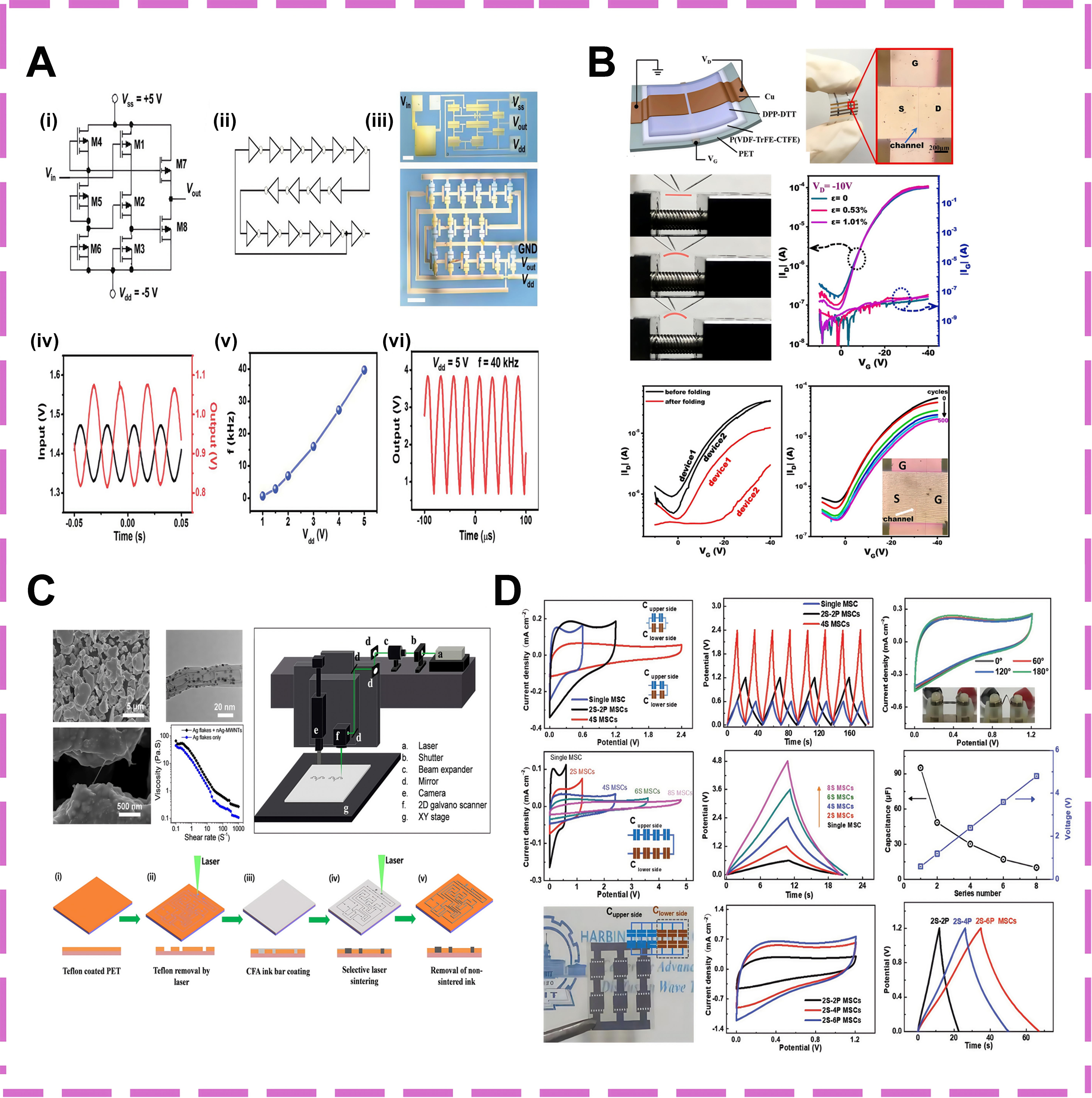
Figure 6. Etching techniques for fabrication and performance characterization of flexible electronic circuits. (A) (i and ii) Circuit diagrams of a cascade amplifier (i) and a fifteen-stage CMOS RO (ii). (iii) Photographs of the cascade amplifier (top) and the CMOS RO (bottom). The scale bars in the panels denote 100 µm. (iv) Input and output waveforms of the cascade amplifier. (v) Oscillation frequency change of the fifteen-stage RO with Vdd increasing from 1 to 5 V. (vi) Output waveform of the fifteen-stage CMOS RO at Vdd = 5 V[59]; (B) Flexible organic transistor on PET substrate[60]; (C) Laser patterning process of the CFA film[61]; (D) Electrochemical performance of MXene DSMSCs in different connection ways[62]. CMOS: Complementary Metal-Oxide-Semiconductor; RO: ring oscillator; Vdd: power supply voltage; PET: polyethylene terephthalate; CFA: carbon conductive flexible adhesive; DSMSCs: double-side microsupercapacitors; GND: ground; DPP-DTT: poly[2,5-(2-octyldodecyl)-3,6-diketopyrrolopyrrole-alt-5,5-(2,5-di(thien-2-yl)thieno-[3,2-b]-thiophene)]; P(VDF-TrFE-CTFE): poly(vinylidene fluoride-trifluoroethylene-chlorotrifluoroethylene); MWNTs: multi-walled CNTs; 2D: two-dimensional; MSC: microsupercapacitor.
In 2013, Dahiya et al. introduced a low-cost flexible packaging strategy that thins silicon chips to 15 μm using tetramethylammonium hydroxide wet etching and transfers them onto PI films via an intermediate PDMS layer, eliminating the need for precision equipment[63]. Under a minimum bending radius of 9 mm, the resistance of metal interconnects exhibited minimal change and remained stable after 1,000 bending cycles, demonstrating excellent electrical robustness and mechanical compliance. In 2021, Sheng et al. focused on controlling lateral undercutting during wet etching by constructing a T-shaped structural model to simulate the etching evolution of an 8 μm copper layer with a 2 μm photoresist under various processing conditions[64]. Their findings revealed that changes in cavity geometry induced recirculation vortices at the bottom, which in turn enhanced lateral etching at the top surface and compromised profile uniformity. Experimental results confirmed that the initial concentration of the etching solution played a decisive role: at 0.45 mol/L, the vertical etch depth reached 7.70 μm, with lateral etching limited to 1.68 μm, yielding an etching factor (EF) as high as 4.58 - a favorable trade-off between vertical selectivity and lateral precision. The optimized process successfully fabricated flexible printed circuit board (FPCB) patterns with an 18 μm line pitch, and atomic force microscopy (AFM) measurements closely matched the simulated morphologies, validating the accuracy of the computational model and providing robust process support for high-density flexible circuit manufacturing. In 2023, Tang et al. introduced a π-shaped copper pattern and applied finite element modeling to analyze flow field and concentration gradient distributions within CuCl2-based wet etching cavities[57]. The study found that increasing the feed speed to 3.8 m/min and nozzle pressure to
While wet etching offers broad material compatibility and uniformity across large areas, its isotropic nature limits boundary precision at sub-micron scales, often leading to lateral undercutting and edge degradation. In contrast, dry etching - characterized by high anisotropy, vertical profile control, and high aspect ratio fidelity - has become essential for fabricating densely integrated flexible circuits, particularly under conditions of complex interconnects, thermal stress, or mechanical strain. As early as 2003, Lindeberg et al. combined double-sided photolithography with dry etching to fabricate nickel nanowire clusters within PI substrates, achieving diameters of 300-500 nm and lengths up to 75 μm[65]. This enabled the creation of an integrated flexible circuit-magnetic sensor platform. Under a magnetic field of 7 kOe, the sensor exhibited a resistance change ratio (ΔR/R) of 0.29%-0.98%, demonstrating excellent magnetoresistive performance. Subsequent oxygen plasma treatment reduced the PI surface contact angle from 59° to 21°, significantly enhancing electrochemical wettability. The device maintained less than 5% resistance fluctuation under a minimum bending radius of 9 mm, and showed no cracking of the metal layers after thermal cycling (25-100 °C), confirming its structural stability and mechanical flexibility under high strain and strong magnetic interference. In 2023, Ouyang et al. extended dry etching applications to multilayer flexible packaging[66]. By integrating through-glass vias (TGVs) into PDMS and applying SF6/O2 plasma for deep reactive ion etching, they achieved an etch rate of 0.49 μm/min with a feature precision of 150 μm. After 1,000 bending cycles at a 2 mm radius, the copper interconnects with 40 μm pitch exhibited only a 7% resistance change, validating the vertical etching capability of plasma dry etching across multi-material interfaces and offering high-reliability process support for flexible packaging under complex deformation environments.
Overall, wet and dry etching technologies serve as complementary approaches in flexible electronics manufacturing, each optimized for distinct structural and application demands. Wet etching offers high selectivity, scalability, and low-cost processing, making it ideal for large-area circuits with relaxed dimensional tolerances. Dry etching, by contrast, enables high-resolution patterning and precise morphological control, supporting the fabrication of high-aspect-ratio microstructures and multilayer heterogeneous systems-key to high-density flexible integration. However, etching processes still face structural challenges. At ultrathin layers or material interfaces, uneven stress release and anisotropic reactions often cause deformation, delamination, or functional failure - undermining device reliability in demanding scenarios such as wearables and integrated sensors.
Looking ahead, etching technologies are expected to evolve along three critical paths. First, green manufacturing will focus on eco-friendly etchants - such as low-toxicity ionic liquids and aqueous solutions - and energy-efficient, low-temperature processes to reduce environmental impact. Second, the integration of multiscale reaction-diffusion modeling with fluid dynamics control will enable precise regulation of interfacial morphology. Third, AI-driven closed-loop platforms will offer real-time monitoring, adaptive parameter tuning, and self-learning capabilities. Through this convergence, etching will shift from a standalone process to a central enabler of structural formation, functional integration, and intelligent, sustainable manufacturing - reshaping the trajectory of flexible electronics fabrication.
Electrochemical etching techniques
Electrochemical etching has emerged as a precise, efficient, and eco-friendly subtractive technique for flexible circuit fabrication. Unlike conventional chemical etching, it enables programmable, maskless patterning via localized electric fields, facilitating high-resolution structuring without extensive chemical usage. By inducing controlled anodic reactions under mild conditions, the method allows selective material removal with minimal environmental impact, making it especially suitable for complex and sustainable flexible electronic systems. In industrial applications, typical patterning resolutions reach 20-25 μm (as reported by TATFOOK), with high-precision features down to 1.6-22.4 μm achievable using meniscus-confined electrochemical etching (MCEE)[60]. At applied voltages of 8-25 V, etch rates generally range from 0.1 to 0.4 μm/min, enabling its deployment in microelectrode fabrication and multiscale channel tuning on flexible substrates[67]. As summarized in Table 4, electrochemical etching has been successfully adapted for a wide range of conductive material systems.
Commonly used materials in electrochemical etching processes for flexible circuits
| Organic materials | Inorganic materials | ||
| Metal | Liquid metal alloy | And other | |
| PEDOT | Copper | Gallium indium alloy | Graphene |
| PANI | Gold | Gallium indium tin alloy | Indium tin oxide |
| PPy | Aluminum | Gallium indium tin zinc alloy | Molybdenum disulfide |
| Silver | |||
| Nickel | |||
As early as 1997, Kaneko et al. proposed a monolithic integration strategy for flexible integrated circuits (ICs) and micromechanical structures, where Complementary Metal-Oxide-Semiconductor (CMOS) circuits were thinned to below 20 μm using KOH-based electrochemical etching and transferred onto a
Electrochemical etching is advancing toward greener processes, intelligent control, and integrated functionality. Environmentally, traditional electrolytes often produce toxic by-products and wastewater, limiting scalability in flexible electronics. To address this, non-toxic and recyclable electrolytic systems have been developed. For instance, electrochemical recovery of indium from waste indium tin oxide (ITO) achieves both high resource efficiency and reduced environmental impact, supporting a sustainable manufacturing chain[70]. Meanwhile, the demand for pattern uniformity and process stability in highly integrated systems is driving the incorporation of real-time monitoring and machine learning into etching workflows. These intelligent feedback systems improve robustness and yield in fabricating complex structures[71]. However, challenges persist in selective etching of multilayer architectures, where interfacial stress heterogeneity and non-uniform corrosion often cause layer warping and microcracking, undermining device reliability. Current strategies, such as electric field modulation and adaptive ion concentration control, aim to mitigate localized stress and enhance structural and functional integrity. As flexible systems evolve to incorporate biodegradable materials, self-healing capabilities, and ultra-low-power wireless modules, electrochemical etching is poised to become a key enabler for sustainable, high-performance, and intelligent flexible electronics.
Laser etching techniques
Laser etching, owing to its non-contact nature, high spatial resolution, and broad material compatibility, is rapidly emerging as a core subtractive manufacturing technique for micro/nano patterning in flexible electronics. In contrast to chemical and electrochemical etching methods that rely on liquid-phase environments and mask systems, laser etching utilizes a focused beam to induce localized, instantaneous ablation. This enables greater design flexibility and compatibility with heterogeneous and multilayered structures. Representative laser direct writing techniques can achieve sub-10 μm spatial resolution[72], processing speeds up to 100 mm/s[73], and a heat-affected zone confined within ~1 μm[74]. Unlike traditional chemical etching which depends on masking and material selectivity, laser etching enables “maskless and geometry-adaptable” patterning by triggering localized ablation, bond breaking, or material vaporization through a high-energy focused laser beam[75]. However, nanosecond or picosecond laser systems often suffer from excessive energy input, which can enlarge the HAZ and lead to edge melting, microcracks, or interfacial delamination - compromising resolution and structural integrity[76]. To overcome these limitations, femtosecond lasers have emerged as a critical breakthrough. Due to their pulse durations being shorter than the thermal relaxation time of materials, they enable ultrafast energy deposition and material removal with negligible heat diffusion - realizing true “cold ablation”.
In 2016, Zacharatos et al. integrated laser direct write (LDW), spatial beam shaping, and selective etching technologies to fabricate continuous silver nanoparticle patterns over areas larger than 1 cm2 on PI, PET, and polyethylene naphthalate (PEN) substrates[72]. The sintered silver films exhibited low resistivity down to
As flexible electronics demand higher integration density, lower power consumption, and adaptability to complex geometries, laser etching is evolving into a core manufacturing platform - integrating subtractive processing, material modulation, and interfacial engineering. Femtosecond and picosecond lasers, with their high spatial resolution and minimal thermal damage, have proven essential for microstructuring ceramics, glass, and polymers in heterogeneous systems. With increasing commercial availability and system reliability, laser etching is transitioning from lab-scale experimentation to pilot-scale manufacturing, showing strong adaptability across diverse processing environments. Looking ahead, the convergence of intelligent modeling, in situ monitoring, and multi-wavelength control will drive the development of adaptive digital fabrication platforms. Real-time tuning of power, focus, and pulse dynamics will enable high-fidelity via formation, edge passivation, and complex multilayer patterning - meeting the demands of heterogeneous integration.
Photolithography techniques
Photolithography has evolved into an indispensable paradigm in micro- and nanofabrication, driving the progression of microelectronics and ICs since its inception. Distinguished by its unrivaled resolution, fidelity, and technological maturity, it underpins the fabrication of high-density interconnects and high-frequency devices[79]. The process operates by projecting light through a mask onto a photoresist, with exposure, development, etching, and lift-off collectively ensuring faithful transfer of nanoscale information onto substrates[80]. Variants of lithography address complementary needs: electron-beam lithography achieves sub-10 nm resolution at limited throughput; focused-ion-beam lithography excels in nanoscale prototyping; extreme ultraviolet (EUV) lithography has enabled scaling at the most advanced semiconductor nodes; while soft lithography, celebrated for low cost and versatility, has expanded applications to nonplanar and flexible substrates[81]. Consequently, photolithography is no longer confined to silicon but is rapidly extending into flexible and multifunctional devices, reinforcing its role as a strategic pillar of cross-platform manufacturing.
In flexible electronics, however, substrate adaptability remains a defining challenge. Conventional techniques exploit the atomically smooth surfaces of silicon wafers, whereas spin-coated resists on polymeric or stretchable substrates exhibit thickness irregularities and edge collapse, eroding pattern resolution and consistency. Addressing this, industry has advanced low-temperature photoresists (< 85 °C) and elastomer-modified systems, exemplified by the formulations of Fuyang Sineva New Material Technology Co., Ltd. (Fuyang Sineva) tailored for organic light-emitting diode (OLED) flexible panels, enabling foldable and rollable architectures while preserving uniformity on heat-sensitive substrates. Equally crucial is the interfacial stability between photoresists and metallic layers, which dictates device reliability. Evaporated films are prone to delamination and cracking under cyclic bending; thus, plasma-assisted surface modification and reactive adhesion-promoting layers[82] have been employed, markedly strengthening metal-substrate bonding and ensuring mechanical integrity of multilayer interconnects under dynamic strain.
Since 2006, lithographic innovations have progressively reshaped the landscape of flexible electronics, advancing from low-temperature processing to high-resolution biointegrated devices. Wong et al. pioneered digital lithography by replacing conventional photomasks with inkjet-printed phase-change layers, enabling hydrogenated amorphous silicon (a-Si:H) TFTs fabricated at ≤ 150 °C[83]. The resulting devices achieved mobilities of ~1 cm2/V·s, on/off ratios > 108, and subthreshold swings of 0.5 V/dec, with precision of ±5 μm allowing fabrication of 128 × 128 pixel arrays (75 dpi) on PEN substrates that preserved conductivity under bending. In 2019, Tang et al. harnessed soft nano-lithography to fabricate highly ordered poly(3,4-ethylenedioxythiophene):poly(4-styrenesulfonate) (PEDOT:PSS) nanowire arrays on PET substrates, with ~70 nm width and ~60 nm height, bridging ~500 nanowires per electrode pair[84]. The process eliminated etching and transfer, achieved 95% yield across 20 devices, and produced flexible ammonia sensors with 100 ppb detection limits, linear sensitivity of 0.2524 ppm-1, and durability beyond 1,200 bending cycles. In 2022, Dadras-Toussi et al. demonstrated multiphoton lithography (MPL) for 3D-printed organic semiconductor composites, where incorporation of 0.5 wt% PEDOT:PSS raised conductivity by ten orders of magnitude to 2.7 × 10⁴ S/m while retaining 89% transmittance at 550 nm[85]. MPL enabled fabrication of ~400 nm resolution circuits and capacitors with specific capacitance of 0.08 F/g, and even preserved enzyme bioactivity, as in glucose oxidase (Gox)-integrated electrodes achieving glucose detection at 0.03 mM, 232.9 µA·mM-1·cm-2 sensitivity, and ~4 s response. Microelectrodes further reduced impedance from 63 to 19 kΩ at 1 kHz, confirming superior electrochemical performance. In 2023, Zschieschang et al. underscored the role of lithography in scaling organic thin film transistors (OTFTs), demonstrating devices with 1.5 μm channels, 1 μm overlaps, mobility of 11 cm2/V·s, transconductance of
Although photolithography remains foundational to flexible electronics, its broader adoption is constrained by its dependence on planar substrates and the intrinsic vulnerability of photoresists under extreme humidity, temperature, and high mechanical loading. These limitations sharply contrast with the pressing demands of wearable and soft electronic systems, where nonplanar architectures, environmental resilience, and mechanical adaptability are indispensable. Progress, however, is converging toward solutions: low-temperature curable and biodegradable resists promise compatibility with flexible substrates; hybridization with inkjet printing, laser direct writing, and transfer methods enables patterning on curved and dynamic surfaces; and real-time monitoring powered by machine learning provides closed-loop control under fluctuating conditions. Looking forward, photolithography is evolving beyond a resolution-centric paradigm to serve as a strategic enabler of flexible, sustainable, and environment-resilient manufacturing. Within emerging domains such as flexible photonics, wearable bioelectronics, and multiphysics-coupled systems, its role is increasingly defined not only by precision but by its capacity to sustain functionality under extreme environments.
Under extreme service conditions, subtractive manufacturing demonstrates unique advantages in constructing highly reliable interconnects through stringent control of pattern fidelity and heat-affected zones. For instance, laser etching effectively suppresses dielectric damage induced by localized overheating, thereby preserving signal integrity in high-frequency circuits. Such processes are particularly critical in aerospace and high-frequency electronics, where devices must endure prolonged exposure to thermal cycling between -55 and 150 °C and sustained mechanical vibrations, with reliability typically assessed in accordance with the Automotive Electronics Council (AEC) standard AEC-Q100. Key evaluation metrics include linewidth uniformity, interfacial adhesion strength, and thermal cycling lifetime, which collectively capture the long-term operational stability of flexible circuits under coupled thermal stresses and complex mechanical loading (JESD22-A104).
Additive manufacturing
Additive manufacturing, initially developed for high-precision electronics, has become integral to flexible circuit fabrication due to its efficiency in material usage, design flexibility, and digital process control. Unlike subtractive methods, it enables direct patterning on flexible substrates without bulk removal, reducing waste and shortening production cycles. Recent advances, including electrochemical deposition, various printing techniques, and 3D printing, have expanded its capabilities from simple pattern transfer to high-resolution, digitally programmable fabrication. These innovations support complex, high-density circuitry while aligning with sustainable manufacturing goals.
Electrochemical deposition techniques
Electroplating techniques
Electroplating has emerged as a key enabling technology in flexible electronics due to its maturity and stability in depositing conductive materials. By electrochemically depositing highly conductive metal layers onto flexible substrates, electroplating offers low resistivity, precise thickness control, and strong interfacial adhesion, making it highly advantageous in flexible circuit fabrication[88]. Unlike subtractive manufacturing, this technique enables direct formation of high-performance circuits without large-area material removal, demonstrating unique competitiveness in high-resolution, multilayer, and complex device architectures[89]. State-of-the-art processes have achieved copper layers with line widths/spacing of 25 μm and thicknesses of 10-20 μm[90], delivering excellent electrical performance and structural stability. As illustrated in Figure 7, electrochemical deposition plays a vital role in the fabrication of multilayer metal architectures and is widely adopted in flexible sensors, wearable heaters, and patterned electrodes. Its contributions to enhancing conductivity, mechanical integrity, and operational reliability are particularly significant in high-reliability applications.
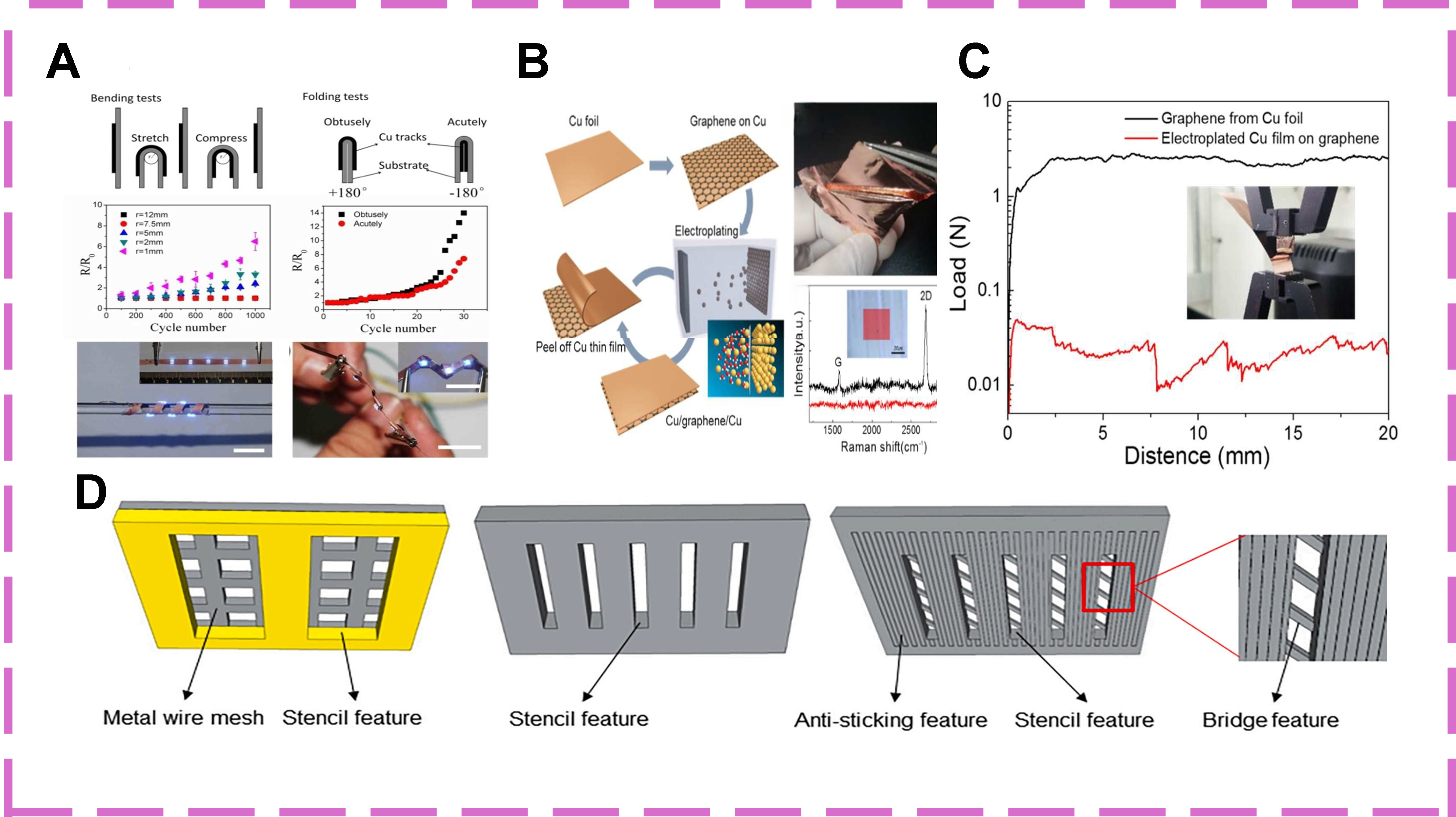
Figure 7. Electrochemical deposition techniques for fabrication, interfacial evaluation, and patterning optimization of flexible electronic circuits. (A) Flexibility and foldability test results of p-Cu circuits on PET substrate[91]; (B) Free-standing Cu thin film from an electroforming process[92]; (C) Comparison of the graphene peel strength from the electroplated Cu and the Cu foil template. For the delamination of Cu film from graphene and CVD graphene from the Cu foil, an epoxy adhesive was used[92]; (D) Comparison of conventional metal masks and HFMM for the screen printing process[93]. PET: Polyethylene terephthalate; CVD: chemical vapor deposition; HFMM: hybrid fine metal mask.
In 2009, Lee et al. systematically evaluated the synergistic effects of current density (0.2-3 A/dm2) and plating time on copper microstructure evolution in flexible laminates[94]. They revealed a preferred orientation transition of copper grains from (220) to (111), which significantly enhanced ductility and stress relaxation. Therefore, the copper layers exhibited exceptional fatigue resistance and electrical stability, maintaining crack-free surfaces and a resistivity of 20.6-22.1 nΩ·m after over 15,000 bending cycles. At high current densities (3 A/dm2), the plating time was reduced to 0.5 h. In 2012, Wu et al. constructed high-density copper patterns with 25 μm line width/spacing on 12.5 μm-thick PI substrates using a process that combined copper adhesion layer evaporation, photolithography, and electroplating[90]. The copper thickness was tunable from 2 to 15 μm (2-10 mA current, 200-1,000 s plating time), and the resulting structures exhibited excellent uniformity and interface bonding. Failure analysis identified local overplating and edge non-uniformity - caused by excessive current density and Cu particle agglomeration (1-5 μm) - as the main sources of short circuits. These issues were effectively mitigated through magnetic stirring and additive optimization, producing defect-minimized copper layers with high purity. The fabricated devices withstood solder float tests (300 °C × 10 s) under 0.7 kgf/cm peel strength and 1015 Ω·cm insulation resistance. In 2015, Liu et al. developed a cost-effective Zn-Cu synergistic process combining galvanic replacement and subsequent electroplating to fabricate flexible copper wires[91]. By using zinc nanoparticle epoxy paste as a seed layer, the initial conductive copper layer (g-Cu) was formed without palladium catalysts or organic reducing agents, followed by electroplated copper thickening (p-Cu). The resulting structure exhibited a low resistivity of ~10-5 Ω·cm, approaching bulk copper levels. The copper wires maintained electrical conductivity after 1,000 bending cycles and 500 thermal shock cycles from -40 to 125 °C, demonstrating excellent mechanical flexibility and environmental reliability. With a minimum pattern resolution of
Electroplated structures in flexible electronics remain prone to microcracks and interfacial delamination under mechanical stress and cyclic loading, severely compromising device reliability. Conventional metallic coatings often suffer from poor fatigue resistance and weak adhesion, limiting their applicability in high-strain environments. To overcome these limitations, composite coatings, such as Cu-graphene and Cu-Ni, have demonstrated improved ductility, fatigue endurance, and electrical performance[96,97]. Concurrently, the integration of automated current modulation and in-situ monitoring has enhanced layer uniformity and reduced morphological defects during electroplating[98], For instance, in a 3.5 wt% NaCl environment, a KF-99-modified graphene oxide-polymer composite reduced corrosion current density significantly[99]. Electroplating is now evolving into a multifunctional platform that combines material innovation, structural tuning, and AI-assisted process control. The incorporation of 2D materials such as graphene and MoS2 boosts conductivity and interfacial strength, while intelligent feedback systems ensure defect minimization and uniform deposition. As device architectures grow increasingly complex, managing interfacial stress and improving interlayer adhesion are critical to prevent fatigue failure. In parallel, the pursuit of green electroplating - via low-toxicity electrolytes and closed-loop deposition - will support sustainable and high-performance flexible electronics.
Electroforming techniques
Electroforming is increasingly recognized as a transformative additive manufacturing process in flexible electronics, enabling the direct construction of intricate metallic architectures through precision-controlled, template-assisted electrochemical deposition. Characterized by its ability to produce high aspect ratio structures, achieve micron-scale pattern fidelity, and maintain superior electrical conductivity, electroforming has transcended its traditional prototyping role to become a cornerstone of pattern transfer in advanced device fabrication[100]. Unlike conventional electroplating, which prioritizes planar uniformity and large-area metal layer formation, electroforming allows for fine-tuned control over structural thickness, morphology, and composition by leveraging parameters such as current density, electrolyte formulation, and temperature gradients[101]. When coupled with micro/nano-lithographic techniques, this process excels in replicating high-resolution features and is particularly suited for fabricating flexible OLED masks, nested microsystems, and 3D functional elements such as microneedle arrays[93]. These electroformed components often exhibit complex 3D topologies and higher aspect ratios than electroplated films, which remain confined to 2D profiles emphasizing adhesion and surface smoothness.
In 2014, Laine-Ma et al. first proposed a pattern transfer method using a releasable carrier, where high-precision copper features with 65-85 μm linewidths were fabricated on stainless steel templates and transferred to thermoplastic substrates such as acrylonitrile butadiene styrene (ABS) and polyphenylene oxide (PPO) via thermal lamination, following surface oxidation using acidic H2O2-H2SO4 treatment[102]. This process achieved an interfacial adhesion strength of 1.4 N/mm and constrained PPO substrate deformation within ±0.1 mm, effectively mitigating thermal stress accumulation and delamination risks - offering reusability, etching-free operation, and dimensional stability. In 2016, Rho et al. introduced a monolayer chemical vapor deposition (CVD)-graphene interface template for electroforming, enabling defect-free copper film detachment due to graphene’s low interfacial adhesion and high conductivity[92]. The resulting copper layers maintained stable sheet resistance (~0.7 Ω/sq) even after 5,000 bending cycles at a curvature radius of 7 mm, with a peel strength of 486.8 ± 36.2 N/m. This study highlights how graphene serves as a release layer that allows uniform Cu thin films to be peeled off without cracks or wrinkles. Mechanical delamination tests revealed that copper deposited on graphene required significantly lower force to separate compared with conventional Cu foil, confirming the weak adhesion at the graphene-Cu interface [Figure 7B and C]. In a 2020 review, Zhang et al. systematically summarized two decades of advances in precision micro/nano-electroforming, highlighting breakthroughs in photolithography-deposition-release workflows, including electrolyte formulation, grain control, and interfacial uniformity[103]. To extend the lifetime and resolution of electroformed masks in high-precision applications, in 2021, Chung et al. proposed a hybrid fine metal mask (HFMM) strategy combining micro/nano-lithography with electroforming[93]. By incorporating bridge-reinforced structures and anti-adhesive coatings, the HFMM exhibited high mechanical strength and release efficiency, with a surface water contact angle of 145°, facilitating < 10 μm pattern transfer. It retained high delamination efficiency and edge fidelity over multiple deposition cycles, proving especially suitable for high-resolution, large-scale production in flexible electrodes and OLED displays. Unlike conventional wire-mesh masks that suffer from pattern distortion and poor release, HFMM introduced stencil and anti-sticking features that significantly improved resolution and durability. The bridge-reinforced design further prevented collapse of fine openings during repeated use [Figure 7D]. More recently, in 2024, Srivastava et al. proposed a cost-effective method for fabricating flexible circuits using graphite-drawn paths followed by copper electroplating[104]. The fabricated copper conductors exhibited stable electrical resistance (~20 Ω) across 25-85 °C, and maintained less than 2.5% variation during ±180° bending. Even after 1,000 bending cycles, resistance increased only from 2 to 2.2 Ω, with less than 10% relative change, indicating superior flexibility and electrical robustness. Long-term durability was also confirmed, with resistance increasing from 3 to just 3.4 Ω over 12 months of ambient storage. This approach enabled the creation of a functional flexible piano circuit with real-time touch response under bending, a bendable light-emitting diode (LED) display (> 85°), and a detailed copper-plated Indian Institute of Technology (IIT) Mandi logo that remained conductive beyond 90° deformation.
Electroforming is advancing into a precision, cost-efficient, and intelligent manufacturing technology with expanding utility in flexible electronics. Integrating 2D materials, such as WS2 and graphene, has notably enhanced the electrical conductivity, mechanical resilience, and interfacial adhesion of electroformed layers. These hybrids enable nanoscale conductive networks with improved structural stability. Concurrently, AI and machine learning are being deployed to monitor deposition in real time, reduce defects, and ensure batch consistency, while self-healing materials extend device reliability under dynamic conditions. To mitigate stress-induced instability in complex architectures, recent approaches include gradient layers, stress-buffering interfaces, and hierarchical structuring - jointly improving mechanical robustness and functional durability. Green manufacturing is also gaining momentum through the development of non-toxic electrolytes and recyclable deposition systems. Furthermore, 3D electroforming, enabled by precise template and rate control, supports the fabrication of spatially complex, high-density interconnects. As materials engineering, intelligent control, and multi-process integration converge, electroforming is poised to become a foundational enabler for next-generation smart, sustainable, and large-area flexible electronics.
Printing techniques
Screen printing techniques
Screen printing, as a low-cost, structurally simple, and highly material-compatible additive manufacturing technique, is rapidly emerging as a mainstream patterning method in flexible electronics. Its working principle relies on stencil-based transfer - where conductive inks are pressed through a patterned mesh screen onto the surface of a flexible substrate using a squeegee - to achieve highly uniform conductive structures[105]. Compared to traditional processes, screen printing eliminates the need for high-vacuum environments and expensive equipment, significantly reducing capital costs and fabrication barriers, especially for large-area and cost-sensitive production[106]. One of its core advantages lies in the controllability of pattern thickness and morphology. By rationally designing the mesh structure and tuning ink rheology, screen-printed patterns with thicknesses ranging from 5 to 50 μm and resolutions better than 100 μm can be realized on various flexible substrates. Metal-based inks such as nano-silver can be sintered at low temperatures (< 150 °C), while carbon-based and hybrid systems form continuous conductive networks via film formation or photo-/thermo-assisted processing, minimizing thermal damage to sensitive materials and enhancing the flexibility and mechanical integrity of the entire structure. As illustrated in Figure 8, printed electronics enable the precise patterning of conductive inks and the multilayer integration of high-performance flexible devices.
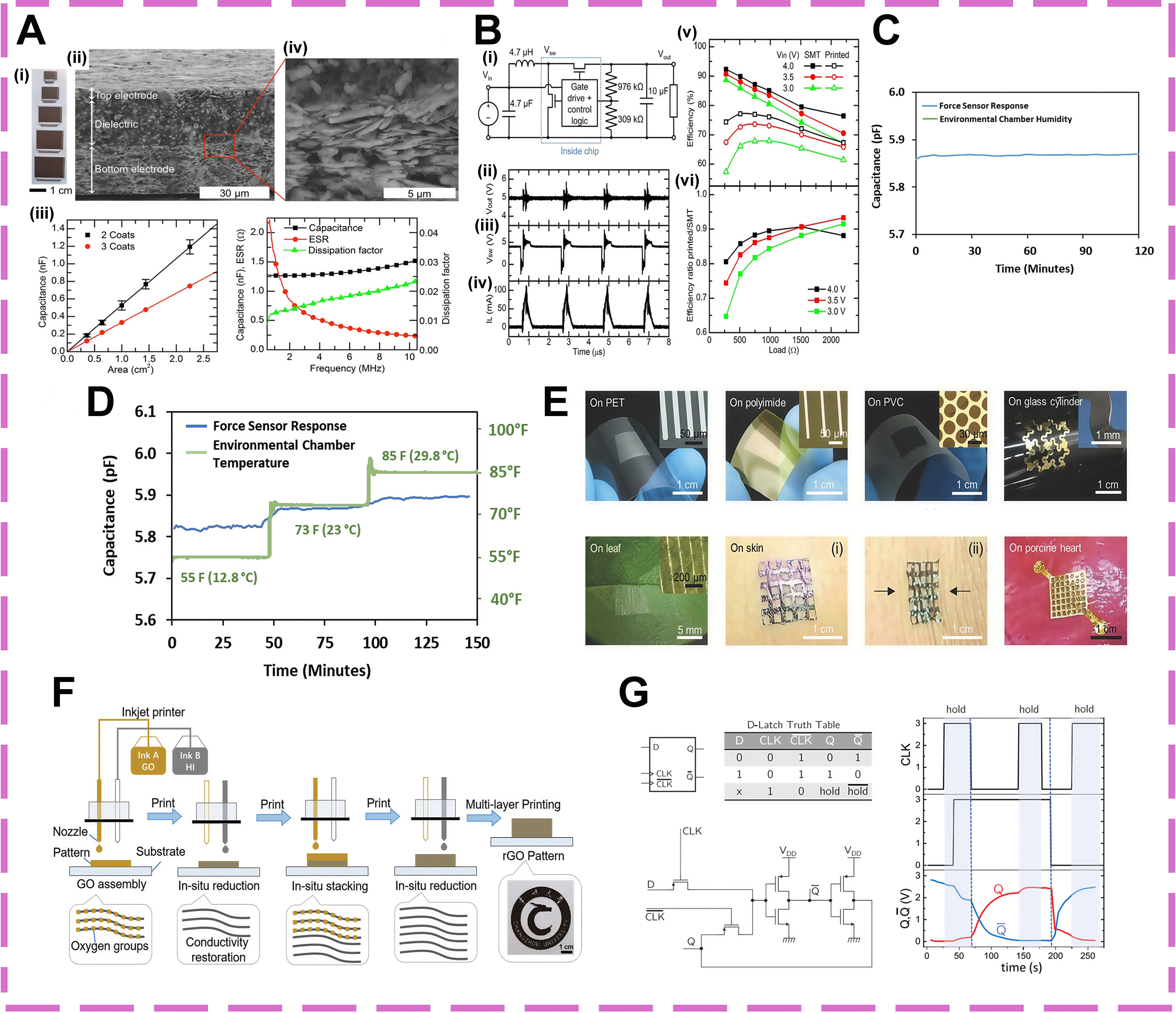
Figure 8. Printing techniques for fabrication, environmental stability, and functional integration of flexible electronic circuits. (A) (i) Photographs of the capacitors with five different areas. (ii) Cross-sectional SEM micrographs of a capacitor with two coats of dielectric, showing the barium titanate dielectric and silver electrodes. (iii) Capacitance of capacitors with 2 and 3 coats of barium titanate dielectric and varying area, measured at 1 MHz. (iv) Capacitance, ESR, and dissipation factor of a 2.25 cm2 capacitor with 2 coats of dielectric, vs. frequency[107]; (B) (i) Diagram of voltage regulator circuit. (ii-iv) Waveforms of (ii) Vout, (iii) Vsw and (iv) current into the inductor, with 4.0 V input voltage and 1 kΩ load resistance, measured using printed inductor. Surface mount resistors and capacitors were used for this measurement. (v) Efficiency of a voltage regulator circuit using all surface-mount components vs. one with printed inductor and resistors, for various load resistances and input voltages. (vi) Ratio of efficiencies of the surface-mount and printed circuits shown in (v)[107]; (C) Effect of relative humidity varying from 20% RH to 80% RH on the force sensor[108]; (D) Effect of temperature on the force sensor[108]; (E) Different thin film devices transfer-printed onto the surfaces of various substrates[109]; (F) A schematic illustration of the in situ approach combining patterning and in situ reduction of GO patterns using reactive inkjet printing[110]; (G) Flexible hybrid complementary-PTL D-Latch on paper[111]. SEM: Scanning electron microscopy; ESR: equivalent series resistance; RH: relative humidity; GO: graphene oxide; PTL: pass transistor logic; SMT: satisfiability modulo theory; PET: polyethylene terephthalate; PVC: polyvinyl chloride; rGO: reduced graphene oxide.
In 2011, Kim et al. conducted an environmental aging test on screen-printed silver circuits under 85 °C/85% RH for 1,000 h, revealing a ~48% decline in flexibility[112]. Their study identified microstructural degradation and resistance fluctuation induced by humid heat as critical limiting factors for silver ink adaptability. The endurance test further showed that smaller bending radii accelerated resistance growth, underscoring the vulnerability of screen-printed Ag circuits to coupled thermal-mechanical stresses. These findings highlight that although silver inks are initially attractive for flexible circuits, their long-term stability under harsh environments remains a key bottleneck. In 2014, Cao et al. employed screen printing to fabricate TFTs based on separated single-walled CNTs (s-SWCNTs), achieving high carrier mobility (7.67 cm2/V·s), high on/off ratios (104-105), and low operating voltages (< 10 V), while maintaining stable performance under a bending radius of 3 mm - demonstrating the excellent adaptability of carbon-based materials for high-performance flexible devices[113]. The study further confirmed that printed inductors integrated into voltage regulator circuits could deliver stable output signals with minimal waveform distortion. Efficiency testing revealed that although printed passive components performed slightly below conventional satisfiability modulo theory (SMT) devices, they still maintained over 80% of the reference efficiency [Figure 8A and B]. In 2015, Ostfeld et al. printed high-Q planar spiral inductors (Q ≈ 33-35, f_res ≈ 24-36 MHz) and resistors, which were integrated into a flexible direct current (DC)-DC boost converter to drive OLED devices[107]. The system achieved a conversion efficiency exceeding 85% under a 4 V input and 1,000 Ω load, outperforming conventional SMT approaches and showcasing advantages for high-frequency, low-power integrated systems. In 2020, Maddipatla et al. developed a screen-printed capacitive force sensor based on silver ink and PDMS, which exhibited excellent linearity [0-100 N, the coefficient of determination (R2) = 0.998], fast response (3.7 s), quick recovery (5.7 s), and good operational stability under 20%-80% RH conditions[108]. The study further showed that humidity variations had negligible impact on capacitance, confirming the sensor’s robustness against environmental moisture. Temperature effects were also systematically evaluated, with stable output maintained across a broad range of 12.8-29.8 °C [Figure 8C and D]. As device complexity increases, system-level integration is becoming a critical frontier in printed flexible electronics. In 2021, Liu et al. proposed a graphene/carbon black hybrid ink strategy, forming a synergistic conductive network that achieved a conductivity of 2.15 × 10⁴ S/m at a linewidth of 90 μm and a thickness of 7 μm[114]. After 1,000 high-strain bending cycles, resistance changes remained below 1.5%, highlighting its mechanical robustness and flexibility. In 2022, Brooke et al. combined vapor phase polymerization (VPP) with screen printing to fabricate poly(3,4-ethylenedioxythiophene) (PEDOT)-based conductive patterns on PET substrates, achieving a conductivity of 500 S/cm and a pattern resolution of 100 μm[115]. The resulting organic electrochemical transistor (OECT) devices demonstrated an on-state current of ~70 mA at 1 V, response times under tens of milliseconds, and transconductance over 100 mS - suitable for high-speed flexible analog circuits. In 2023, Qin et al. systematically reviewed the development of carbon-based conductive inks and printing techniques, emphasizing their synergistic optimization for high conductivity, low cost, and environmental robustness[116].
Despite the significant advantages of screen printing in terms of cost-effectiveness and production scalability for flexible electronics, it still faces critical limitations in achieving high-resolution and high-density circuitry[117]. To overcome this precision barrier, researchers have introduced high-tension polyester mesh screens and optimized ink rheological properties, such as viscosity and surface tension, to enhance pattern fidelity[118], thereby expanding the applicability of screen printing to micro-scale patterning. Beyond resolution, long-term mechanical fatigue and electrical instability of printed patterns also pose significant reliability concerns. To address issues such as microcrack formation and conductivity degradation, self-healing ink systems have recently emerged. For example, polymeric inks embedded with microcapsules can autonomously repair conductive pathways upon fracture[119]. In parallel, the integration of conductive nanocomposites continues to advance, with functionalized ZnO-reduced graphene oxide (rGO) and MWCNT-based composites showing outstanding performance in enhancing both electrical conductivity and mechanical durability[120,121]. In line with green manufacturing and hybrid integration trends, efforts are underway to develop biodegradable inks and integrate screen printing with techniques such as laser direct writing and electrochemical deposition. This convergence promotes a more sustainable, versatile manufacturing platform capable of meeting regulatory demands and system-level integration needs. Screen printing is poised to play a central role in next-generation flexible electronics - enabling multifunctional, durable, and eco-friendly smart devices.
Thermal transfer printing techniques
Thermal transfer printing has emerged as a key technique in flexible electronics manufacturing due to its efficiency, versatility, and cost-effectiveness[122]. Unlike screen printing, which relies on direct deposition through patterned masks, thermal transfer decouples pattern formation from material deposition. High-precision conductive patterns can be prefabricated on donor films and then rapidly transferred to the target substrate via thermal lamination, significantly improving pattern fidelity and interfacial integrity. Typically performed at ~180 °C under ~5 kg/cm2 pressure, the process facilitates softening, melting, or interfacial reactions of the functional materials, enabling pattern transfer onto heat-sensitive substrates such as PET and textiles, with achievable resolutions down to 40 μm[123]. Compared to screen printing, which is sensitive to stencil precision and ink rheology, thermal transfer offers superior thermal stability and interfacial adaptability, making it particularly suitable for low-temperature-compatible fabrication. Moreover, the process requires no high-energy equipment or complex post-processing, thereby reducing manufacturing time, material waste, and overall costs[109].
In 2018, Descent et al. proposed a donor-film-based thermal transfer method that efficiently transfers a
Thermal transfer printing is evolving into a low-temperature, multifunctional, and intelligent manufacturing technique with expanding potential in flexible electronics. The incorporation of advanced conductive materials, such as liquid metals and graphene, alongside refined microstructural tuning has significantly improved the electrical and mechanical performance of printed layers. The emergence of sub-50 °C transfer processes has enhanced compatibility with heat-sensitive substrates, including polymer films and textiles, minimizing thermal damage and broadening application scope. Meanwhile, AI and big data are enabling intelligent control through real-time monitoring and dynamic thermal feedback, improving consistency and yield in large-scale production. To boost mechanical resilience and stretchability, self-healing materials have been introduced, allowing conductive patterns to recover function after cracking or fatigue, thereby extending device longevity. Additionally, stress-distribution optimization and low-modulus interfacial engineering are being integrated to mitigate multiscale stress concentrations and enhance structural stability in system-level applications. As flexible electronics shift from 2D patterning to 3D integration and complex system architectures, thermal transfer printing is transitioning from a low-cost, rapid process to a platform offering advanced material adaptability, interfacial reliability, and multilayer integration. Driven by green manufacturing and hybrid process demands, it is poised to play a pivotal role in next-generation flexible electronic fabrication.
Inkjet printing techniques
Inkjet printing is rapidly advancing as a transformative additive manufacturing technology in flexible electronics, underpinned by its non-contact deposition modality, fully digital control architecture, and superior material utilization exceeding 90%[126]. Thermal inkjet systems typically eject droplets of approximately 23 pL with diameters around 35 μm, while piezoelectric systems can achieve finer 14 pL droplets (~30 μm in diameter), enabled by nozzles of ~40 μm and operated within a frequency spectrum of 6-30 kHz (Advanced Printing Technologies). When coupled with precise substrate temperature regulation (40-80 °C) and high-precision motion control, this setup enables resolution surpassing 30 μm[127]. Crucially, inkjet printing facilitates real-time pattern customization and multilayer deposition without physical tooling, drastically reducing iteration cycles by over 70% and slashing production costs to merely one-tenth of conventional manufacturing approaches[128]. Unlike screen printing, which depends on stencil templates and viscous paste formulations, inkjet technology is inherently compatible with low-viscosity functional inks, enabling maskless, agile pattern switching-ideal for small-batch, design-variable circuit prototyping. Furthermore, while thermal transfer printing requires prior fabrication on donor substrates followed by entire-pattern relocation, inkjet printing enables direct, on-site deposition with superior topological adaptability[129].
In 2011, Huang et al. developed a water-based graphene oxide (GO)/functionalized GO (FGO) ink formulation, enabling the fabrication of flexible conductive patterns through 25-pass multilayer printing followed by thermal reduction at 400 °C[130]. The resulting structures exhibited a conductivity of up to
Inkjet printing is advancing toward higher precision, enhanced multifunctionality, and environmentally sustainable manufacturing. Nanomaterial-based inks - such as MoS2 dispersions - combined with AI-assisted optimization of jetting frequency and droplet control are pushing patterning resolution to the submicron scale, enabling high-density fabrication in flexible electronics. In parallel, biodegradable inks derived from cellulose and other natural polymers align well with inkjet printing’s low-energy, mask-free process, supporting green manufacturing and reducing ecological impact. Functionally, inkjet printing allows precise multilayer stacking and the direct integration of energy devices like supercapacitors and self-powered modules - addressing growing demands for lightweight, highly integrated, and energy-autonomous systems in wearables and IoT. Future integration of big-data-enabled in-situ monitoring and intelligent automation will further close the loop between design and production, promoting large-scale deployment of cost-effective, high-performance flexible electronics. Inkjet printing is thus emerging as a key platform in next-generation intelligent electronics. To meet the rising demand for stretchable, reliable interconnects, liquid metal wiring offers a material-driven solution with superior conductivity retention under extreme deformation[133].
Electrospinning techniques
Electrospinning (ES) has evolved into a transformative nanomanufacturing paradigm that seamlessly integrates operational simplicity with exceptional material adaptability, enabling the rational design of nanofiber networks with finely tailored dimensions and architectures. Its distinctive capability to engineer functional structures at the micro- and nanoscale has rendered it indispensable in frontier domains such as flexible electronics, biomedicine, filtration, energy storage, and catalysis[134]. The underlying mechanism involves the generation of a Taylor cone at the needle tip of a polymer solution or melt under a strong electric field, where the charged jet undergoes continuous stretching and thinning. Subsequent rapid solvent evaporation or melt solidification produces uniform and highly controllable micro/nanofiber membranes on the collector[135]. These membranes are characterized by extraordinarily high surface-to-volume ratio, porosity, and tunable alignment, while parameters such as voltage, flow rate, and collection distance allow precise modulation of fiber diameter, morphology, and distribution[136]. Industrial scalability has been convincingly demonstrated by Innovative Engineering Solutions (Inovenso, Turkey), whose NanoSpinner 416 Industrial Electrospinning/Spraying Line fabricates nanofibers with diameter precision between 0.05-0.4 μm (average ~120 nm), employing 132-264 nozzles and achieving web widths of up to 100 cm, thereby underscoring the industrial readiness of ES for large-scale flexible electronics.
Unlike conventional techniques, ES uniquely enables low-temperature, direct fabrication of 3D porous networks on flexible substrates, simultaneously preserving mechanical compliance and enhancing interfacial tunability - an essential feature for maintaining functional reliability under high strain, humid, and thermally dynamic environments. A representative case is the ES of polyvinylidene fluoride (PVDF), where dipoles (-CH2 and -CF2) align with the electric field, markedly elevating β-phase content and crystallinity, thereby amplifying piezoelectric and dielectric properties[137]. Beyond single-polymer systems, incorporation of conductive or thermally conductive fillers enables electrospun composites to combine mechanical flexibility with efficient heat dissipation, mitigating electromigration and local overheating in high-power interconnects. Notably, boron nitride (BN)/graphene-doped aligned nanofiber membranes demonstrate in-plane thermal conductivities exceeding 3 W·m-1·K-1 with thicknesses below 50 μm, offering a viable solution for thermal management in high-density circuits[138]. Concurrently, the adoption of sustainable strategies has extended ES into green electronics, where cellulose nanofibers and lignocellulosic nanofibers produce membranes with superior mechanical robustness and barrier performance, significantly reducing WVTR, suppressing moisture-induced dielectric drift and insulation degradation, and enabling environmentally responsible disposal upon end-of-life[139].
Since 2021, ES has catalyzed a series of breakthroughs in flexible electronics and energy devices, demonstrating its disruptive potential across materials and applications. Wang et al. pioneered a liquid-metal stencil printing strategy using electrospun thermoplastic polyurethane (TPU) nanofiber membranes, achieving layer-by-layer ICs that combined ultrahigh conductivity (3.2 × 10⁴ S/cm), extreme stretchability (stable LED illumination at 800% strain), excellent breathability (814 L/m2/s), and chemical durability[140]. The resulting strain sensors delivered segmented linear responses across 0%-200% strain [gauge factors (GFs) 1.35 and 2.69], while capacitive arrays enabled real-time 4 × 4 tactile mapping with recyclability and reconfigurability. In 2023, Ilango et al. underscored the decisive role of ES in flexible batteries, where one-dimensional nanofiber networks provided enlarged surface area, high porosity, and tunable architectures, drastically shortening ion diffusion pathways and enhancing cycling stability[141]. Si/CNF composite electrodes retained 869 mAh/g after 480 cycles, SnOx-CNF electrodes delivered 674 mAh/g after 100 cycles, and NiCo2O4/carbon-fiber composites maintained 639 mAh/g after 100 cycles. In 2024, Xie et al. addressed long-standing weaknesses of ceramic paper by developing printable flexible ceramic fiber sheets with
At the application frontier, ES has revealed transformative potential in flexible circuits by advancing encapsulation, reinforcement, and functional separation layers. Poly(vinylidene difluoride-co-trifluoroethylene) [P(VDF-TrFE)]-based electrospun membranes serve as high-performance encapsulation films, uniting low WVTR with intrinsic piezoelectric responsiveness to suppress metal corrosion and leakage[145]. As reinforcement, the porous architectures of electrospun networks effectively dissipate localized stresses, delaying pad uplift and interlayer delamination. In energy storage, PVDF/ceramic nanofiber separators - featuring high porosity and thermal stability - have been extensively validated in lithium-ion batteries[146]. Electrospun electrodes further advance wearable and bioelectronic systems, combining breathability, softness, and biocompatibility to preserve electrical fidelity under continuous skin and tissue deformation[147].
Nevertheless, its reliability under extreme environments remains a formidable challenge. Under high humidity, repeated thermal cycling, and heavy mechanical loading, devices are prone to dielectric drift, interfacial aging, and microcrack propagation, which critically undermine long-term stability. Addressing these limitations will require advanced interfacial engineering strategies - such as core-shell structures and plasma modification - to enhance environmental robustness, alongside multiphysics modeling frameworks capable of capturing coupled electrical, thermal, mechanical, and humidity effects. Moreover, the integration of intelligent control into ES processes promises greater manufacturing precision and reproducibility. Through these innovations, ES can evolve from a laboratory technique into a scalable pathway for producing flexible devices capable of reliable operation in extreme conditions and under high-load demands.
Reverse offset printing techniques
Reverse offset printing (ROP) is rapidly redefining additive manufacturing in flexible electronics, offering a rare convergence of submicron resolution, cost-efficiency, and industrial scalability. Unlike inkjet printing, which relies on stochastic droplet deposition, ROP utilizes an “indirect transfer” strategy: inks first form a continuous film on an elastic blanket roll and are then precisely detached and redeposited onto the substrate. This controlled transfer effectively suppresses deleterious artifacts such as coffee-ring formation and edge roughness, enabling large-area fabrication of uniform submicron-scale features[148]. Cutting-edge studies have demonstrated linewidths below 1 μm[149], dramatically outperforming conventional screen and inkjet printing, while eliminating reliance on costly masks and reducing process complexity, thereby advancing toward scalable industrial adoption[150]. Across domains ranging from flexible displays and TFTs to OLEDs, RFID, and high-frequency antennas, ROP is now recognized as a pivotal manufacturing node that reconciles fine resolution with throughput. At the mechanistic level, its fidelity is governed by ink rheology and the wetting-dewetting dynamics of the blanket interface: typical inks exhibit viscosities near 15.5 mPa·s at 1 s-1 shear rates[151], while transfer pressure and velocity directly dictate edge integrity and dimensional uniformity. These attributes endow ROP with exceptional versatility, accommodating diverse functional inks - including silver nanoparticles, CNT dispersions, graphene, and conductive polymers - and supporting substrates such as PI, PET, paper, and flexible glass.
In 2019, Leppäniemi et al. harnessed ROP to pattern metal nitrate-based oxide semiconductor inks with submicron precision, enabling high-performance flexible TFTs[152]. Oxygen plasma treatment tuned the surface energies of PDMS and substrates, producing In2O3 patterns with linewidths near 1 μm, uniform thicknesses of 15-20 nm, sharp boundaries, and complete suppression of coffee-ring defects. Devices fabricated on Si/SiO2 and PI/Al2O3 exhibited saturation mobilities of 3.1 and 3.5 cm2/V·s with on/off ratios of 107-108, outperforming inkjet-printed counterparts. Structural stability persisted under 300 °C annealing, while Ag electrodes annealed at 250 °C improved conductivity but revealed ion migration risks. Roll-to-roll processing further demonstrated scalable fabrication of continuous ≈ 2 μm lines, confirming ROP’s potential in high-resolution flexible sensing and display technologies for harsh environments. In 2021, Shin et al. advanced tunable ROP using a stretchable PDMS blanket, enabling dynamic scaling of pattern dimensions[153]. By transferring Ag inks in a pre-stretched state and releasing strain, linewidths contracted from 24 to 15.3 μm and spacings from 121 to 69 μm at ε = 1.5. This innovation transcended mold resolution limits, preserved fidelity under extreme strain, and allowed directional control of anisotropic and isotropic patterning. Compared to lithography and inkjet methods, it offered reduced costs, simplified workflows, and scalable precision fabrication of flexible devices suited to sensors, displays, and electronics for extreme environments. In 2022, Kim et al. proposed a streamlined ROP route for micropatterning copper nanowire (CuNW) transparent electrodes with resolutions down to 7 μm[154]. Ink formulations incorporating poly-4-vinylphenol (PVP), propylene glycol monomethyl ether acetate (PGMEA), and polyacrylates optimized cohesion and adhesion, producing sharp, uniform patterns. Intense pulsed light (IPL) annealing reduced sheet resistance to 31.6 Ω/sq with 79% optical transmittance at 550 nm. Devices sustained electrical integrity over 1,000 cycles at 1 mm bending radii and showed < 11% resistance variation after 162 h in ambient conditions. Applications in flexible LEDs, transparent heaters, and OLEDs demonstrated long-term stability and robustness under mechanical and environmental stress. In 2025, Dai et al. pioneered ROP in electroluminescent multipixel arrays, surpassing screen printing in both resolution and luminance[155]. COMSOL-guided designs achieved 200 μm pixels with 100 μm spacing, delivering tenfold brightness gains and peak luminance of 71.9 cd/m2 per pixel. Arrays fabricated under roll-to-roll conditions preserved uniformity and flexibility, operating reliably when bent to 1 cm diameters. By avoiding photolithography and vacuum deposition while offering precise boundaries, ROP demonstrated scalable, durable, and energy-efficient pathways for wearable displays under prolonged mechanical stress. In 2025, Eiroma et al. showcased micrometer-scale Cu wiring and electrodes for flexible circuits via two ROP-based approaches: Cu nanoparticle ink with IPL sintering, and polymer resist ROP combined with vacuum copper deposition and lift-off[156]. Both yielded linewidths of 1-2 μm, thickness uniformity < 5%, and yields exceeding 99%. On 38 μm PI and 125 μm PEN, sheet resistances reached 0.56 Ω/sq, with resistivities approaching bulk copper (4.9-6.3 μΩ·cm). Under severe bending stress, robust chip-to-substrate connectivity was maintained, with nanoparticle-based structures offering superior initial reliability due to enhanced thickness stability.
Fukuda et al. achieved channel lengths down to 0.6 μm in organic TFTs, yielding mobilities of ~9.0 ×
Looking forward, three trajectories are poised to shape the evolution of ROP. First, the development of nanocomposite inks and eco-benign solvent systems will improve both sustainability and long-term device reliability. Second, embedding machine vision and closed-loop control into the transfer process will enable real-time defect detection and correction, enhancing reproducibility and yield. Third, deep integration with other processes will catalyze scalable submicron patterning on large-area flexible substrates, paving the way for applications in flexible displays, wearable healthcare electronics, and high-frequency communication. In essence, ROP’s strategic value resides in its ability to reconcile the dichotomy between resolution and throughput, positioning it as an intermediate yet transformative technology between photolithography and inkjet printing. Future breakthroughs will depend not on incremental parameter tuning alone but on cross-process convergence and intelligent end-to-end automation, propelling flexible electronics manufacturing toward a future of precision, affordability, and sustainability.
3D printing techniques
Fused deposition modeling techniques
As a representative technique in additive manufacturing, fused deposition modeling (FDM) has recently demonstrated significant potential in the construction of flexible electronics. This process involves heating thermoplastic materials - such as PLA or TPU - to 200-300 °C and extruding them through a nozzle to build 3D structures with conductive or insulating functionalities, layer by layer, at thicknesses ranging from 0.05 to 0.3 mm[161]. Typical FDM systems feature a build volume of 200 mm × 200 mm × 250 mm, a dimensional accuracy of approximately 0.2 mm, and positioning precisions of 5.5 μm in the Z-axis and 15 μm in the XY-plane, with a maximum printing speed of up to 150 mm/s. These parameters enable the efficient fabrication of multifunctional support frameworks and embedded conductive architectures. With a simple processing flow, low material cost (< 0.1 USD/g), and high adaptability to various equipment platforms, FDM is particularly suited for the customized, small-batch production of curved and structurally complex electronic devices. Although its resolution is inferior to that of photolithography and screen printing, FDM exhibits unique advantages in geometric design flexibility and material compatibility. Researchers have developed composite filaments by integrating high-conductivity carbon-based materials such as graphene and CNTs[162]. Meanwhile, composite hydrogels with tunable mechanical performance have also emerged as promising FDM-compatible materials for applications requiring both conductivity and stretchability[163]. As illustrated in Figure 9, FDM enables structured, multimaterial fabrication and the direct printing of functional components for a wide range of applications.
Figure 9. 3D printing techniques for curved structure fabrication and multifunctional device integration in flexible electronics. (A) Curved layer vs. flat layer for conductive polymers[164]; (B) Curved layer part produced by modified Fab@home rapid prototyping machine, and curved layer part produced by the National University of Singapore machine[164]; (C) Simplified schematics depicting the process of graphene-based 3D printing using the technique of FDM[165]; (D) Fully-printed, flexible, and hysteresis-free CNT-TFTs[166]; (E) Lathe AJP for smart catheter functionalization[167]. 3D: Three-dimensional; FDM: fused deposition modeling; CNT-TFTs: carbon nanotube thin-film transistors; AJP: aerosol jet printing; PLA: polylactic acid; PLL: poly-L-lysine; SWCNTs: single-walled carbon nanotubes; IPA: isopropyl alcohol; ACE: acetone; PDMS: polydimethylsiloxane.
In 2011, Diegel et al. introduced the concept of Curved Layer Fused Deposition Modeling (CLFDM), which combines nonplanar slicing with continuous path optimization algorithms[164]. This strategy enables the continuous deposition of conductive polymers on complex 3D surfaces, effectively mitigating interlayer discontinuities and the staircase effect commonly seen in conventional FDM. Experimental results demonstrated a ~30% increase in interlayer tensile strength for short wood fiber-reinforced polypropylene, and a 25% improvement in shear strength for glass fiber composites. Compared with flat-layer circuits, CLFDM produced smoother surfaces, stronger interlayer bonding, and more reliable conductive pathways, making it highly suitable for flexible electronics requiring large deformation [Figure 9A and B]. In 2016, Zhang et al. developed a flexible composite filament by blending thermally rGO (600 S/cm) with a PLA matrix for FDM printing[165]. The introduction of r-GO not only enhanced electrical conductivity but also preserved the ductility of the PLA matrix, enabling multifunctional integration. This strategy highlights the potential of combining renewable biopolymers with conductive nanofillers to balance sustainability and performance [Figure 9C]. With a 6 wt% filler content, the composite maintained excellent flexibility, and its conductivity increased to 4.76 S/cm after directional extrusion, outperforming typical carbon-based conductive composites. The resulting flexible circuit exhibited an 800 μm linewidth and strong interlayer adhesion, enabling stable LED operation and showing good adhesion and deformation tolerance on both paper and PI substrates. That same year, Zhou et al. explored a hybrid strategy that combines FDM-printed substrates with inkjet-printed silver nanoparticle traces[168]. They proposed a three-step approach-thermal plowing, high-viscosity ink deposition, and low-temperature sintering-which significantly enhanced the continuity and density of conductive paths on rough FDM surfaces. The silver ink (HPS-021LV) achieved a resistivity as low as 6.94 μΩ·cm after sintering at 125 °C for 20 min, approaching the intrinsic value of bulk silver (5.9 μΩ·cm). Furthermore, the drying time for a 1 μL droplet at 200 °C was reduced to ~100 s, far outperforming aqueous systems. More recently, in 2024, Gupta et al. provided a comprehensive review of extrusion-based 3D printing for wearable electronics[169]. They highlighted recent progress in the fabrication of triboelectric nanogenerators (TENGs), flexible lithium-ion batteries, and strain sensors. These systems have been successfully deployed in monitoring physiological signals such as heart rate, blood pressure, and glucose levels, and are expanding into intelligent packaging and environmental sensing.
Despite the structural design flexibility and manufacturing simplicity of FDM, its broader adoption in flexible electronics remains limited by challenges in electrical uniformity and long-term reliability. The layer-by-layer architecture of FDM makes conductive paths prone to cracking or open-circuit failure under repeated bending, reducing suitability for high-flexibility applications. To address this, CNTs have been incorporated into thermoplastic PU. Meanwhile, interlayer misalignment and uneven thermal solidification inherent to FDM hinder integration precision. To improve fabrication consistency, intelligent control systems have been applied to monitor nozzle temperature and deposition rate in real time. Multifunctional composites, such as r-GO/PLA, have also strengthened interfacial adhesion and fatigue resistance, supporting durable structural performance. Functionally, FDM is evolving toward the direct printing of multi-material, stimuli-responsive, and 3D-integrated devices. In areas like implantable electronics and biodegradable platforms, the use of biocompatible materials and low-temperature processing allows for programmable, environmentally adaptive structures.
Looking ahead, FDM is expected to transcend its limitations through hybrid integration with techniques such as laser sintering and inkjet printing, expanding material compatibility and design complexity. Additionally, green manufacturing chains based on biodegradable materials will support its sustainable application in next-generation flexible electronics. Together, these advances position FDM as a versatile integration platform within future intelligent manufacturing ecosystems.
Aerosol jet printing techniques
Aerosol jet printing (AJP) has emerged as a promising additive manufacturing technique that overcomes the inherent limitations of conventional printing processes. By atomizing liquid precursors and directing them onto substrates via high-velocity gas streams, AJP enables non-contact deposition with minimal thermal input, effectively addressing the constraints of photolithography and screen printing in terms of equipment cost, process complexity, and material compatibility[170]. Compared to layer-by-layer thermal extrusion methods such as FDM, AJP offers superior spatial freedom and micron-level patterning resolution, achieving lateral features as small as 10 μm (Optomec). Furthermore, its compatibility with a wide range of functional inks - including metal nanoparticles, conductive polymers. Notably, AJP has advanced from traditional planar deposition to conformal patterning on 3D surfaces, enabling the continuous fabrication of conductive traces on curved, irregular, and even dynamically deforming substrates[171].
In 2016, Gupta et al. systematically established the critical process window for AJP, elucidating the influence of parameters such as nozzle diameter (150 μm), focusing ratio (4.5), platform speed (5 mm/s), and substrate temperature (45 °C) on line width control and the mitigation of the coffee-ring effect[172]. Their work not only achieved sub-10 μm resolution but also confirmed the compatibility of the printed interconnects with CMOS chips and flexible PET substrates, directly linking printing parameters to device integration quality. Under optimized conditions, the silver ink linewidth was confined to < 10 μm with smooth cross-sectional profiles, and integration of silver ink, Sukhoi-8 (SU-8), and PEDOT:PSS enabled the fully printed construction of passive components including capacitors (10-60 pF), resistors (200-950 Ω), and inductors (1-12.5 nH). Post laser sintering, a sheet resistance of 0.2 Ω/sq was achieved, with excellent deposition uniformity and compatibility demonstrated on both PET flexible substrates and 3D curved surfaces. In 2017, Cao et al. realized fully printed CNT-TFTs using AJP, achieving a high mobility of
Despite significant progress in fabrication capabilities and device performance, AJP still faces key obstacles to large-scale industrial adoption. A primary concern is the poor environmental stability of conductive materials-especially copper-based nanoparticle inks-which are prone to oxidation under ambient conditions, leading to rapid conductivity degradation. Although antioxidant coatings have been explored, their long-term effectiveness under high humidity and elevated temperatures remains unproven. Another critical challenge lies in achieving uniform deposition and high-resolution patterning for multilayer circuits and large-area applications, which limits process scalability. To address this, Smith et al. proposed an optimized process framework involving aerosol parameter tuning and gas flow field control, enabling more stable deposition on complex flexible substrates[174]. However, further improvements in resolution and reproducibility remain essential for realizing high-density interconnects and multifunctional integration in industrial systems[175]. Current research is focusing on the coupled design of interfacial engineering and multilayer architecture. By introducing stress-buffering layers and functionally graded structures, this approach aims to effectively suppress strain concentration and enhance the deformability of printed patterns, thereby advancing AJP toward higher reliability.
Additive manufacturing, represented by deposition techniques, printing processes, and 3D printing, is distinguished by its ability to enable multi-material co-deposition and reconfigurable architectures, thereby demonstrating unique adaptability under extreme environments compared with subtractive approaches. In high-humidity and corrosive conditions, composite inks improve the densification and impermeability of conductive pathways. This strategy has been demonstrated in flexible energy storage devices and implantable bioelectronics, which retain stable performance under 85 °C/85% RH accelerated aging tests (JESD22-A101). Under high mechanical loading, 3D printing allows the construction of embedded or 3D interconnect structures that effectively mitigate stress concentrations, ensuring stable electrical performance in wearable systems and soft robotics. Reliability evaluation is typically conducted in terms of damp-heat endurance (JESD22-A101, IEC 60068) and electrical retention under high-cycle bending (IEC 62899-202-5), which collectively reflect the long-term stability and robustness of additively manufactured circuits operating under coupled environmental and mechanical stresses.
Conformal manufacturing
Conformal manufacturing reconfigures existing materials at the micro- or nanoscale to create functional circuit structures without adding or removing mass. Focusing on spatial modulation and structural adaptation, it emphasizes “normative” rather than “material-intensive” processes. Enabled by smart materials and microscale techniques, conformal approaches-such as self-assembly and laser-induced carbonization-offer maskless, energy-efficient, and highly controlled patterning suitable for multi-material integration and 3D microstructural tuning. As AI-driven design and multi-physics platforms mature, conformal manufacturing is emerging as a key strategy to transition flexible circuits from 2D static layouts to 3D dynamic architectures, enabling synchronized evolution of materials and device functions.
Self-assembly techniques
Self-assembly has emerged as a pivotal conformal manufacturing strategy for constructing flexible electronics, offering a distinct paradigm from conventional additive or subtractive approaches. Rather than relying on material deposition or selective removal, self-assembly guides pre-existing functional units to autonomously organize into ordered architectures under external energy gradients. This mechanism enables maskless, contact-free fabrication patterns and multifunctional structures, particularly advantageous for complex, nonplanar flexible substrates. The fundamental driving forces arise from intrinsic physicochemical potential differences within the material system - including surface tension, electromagnetic response, van der Waals interactions, and capillary forces - which collectively minimize system free energy to achieve spatial configuration optimization and electrical compatibility[176]. With a resolution down to 2 μm, self-assembly demonstrates broad material compatibility and dimensional scalability[177]. To enhance both precision and throughput, recent research has focused on interface-guided strategies based on triple-phase contact line tension control. By modulating the surface energy difference (Δγ) between the liquid medium and the patterned substrate, the functional units can be precisely localized within energy wells, enabling efficient assembly of device modules on non-flat surfaces[178]. As illustrated in Figure 10, the self-assembly process allows automatic construction of complex devices by controlling interfacial energy, stress fields, or template geometries.
Figure 10. Self-assembly techniques for molecular design, structural construction, and functional integration of flexible electronic materials. (A) Various cellulose-based functional materials derived from the molecular-scale design and structural optimization[179]; (B) Schematic illustration of hierarchical structure of cellulose and molecular design strategies for the construction of functional materials[179]; (C) Schematic, mechanism, and characterization of the tension gradient-electrostatic attraction-induced silver colloidal nanoparticle self-assembly strategy[177]; (D) Demonstration and characterization of the nanoparticle microelectronics[177]. PDDA: Poly(dimethyl diallyl ammonium chloride); LED: light-emitting diode.
In 2012, Knuesel et al. proposed a liquid-liquid-solid three-phase interfacial self-assembly strategy driven by surface energy differentials[176]. By carefully tuning hydrophilic [11-mercaptohendecanoic acid (MUA)-modified Au] and hydrophobic [3-glycidyloxypropyl trimethoxysilane (GPTMS)-modified Si] interfaces, the assembly process exploited an energy cascade of up to -400 mJ/m2 to precisely guide chip orientation and attachment. Without gravitational assistance, they achieved rapid and precise positioning of 3-1,000 μm chips on flexible substrates, enabling tight tiling at a lifting speed of 30 mm/s. Within three minutes, 62,000 chips were assembled with a positioning accuracy of 0.9 μm and a yield of 99.3%, significantly outperforming conventional pick-and-place methods. The resulting 20 μm-thick flexible silicon concentrator solar cells retained 90% of their photovoltaic efficiency under a bending radius of 1 cm, reducing silicon material usage by 22-fold compared to traditional 300 μm wafers, and demonstrating strong adaptability to high-curvature, high-integration energy systems. In 2018, Guo et al. introduced a controlled tensile buckling strategy that enables predictable evolution of 2D functional films into 3D mesostructures without requiring pre-stretching[180]. This method accommodates a wide range of materials - including metals, polymers, and semiconductors - and operates across scales from micrometers to centimeters. The out-of-plane displacement reached up to 80% of the feature length. A helical interconnect-LED array integrated using this method demonstrated responsive stepwise illumination under strains ranging from 9.8% to 49.6%, supporting the structural design of reliable strain sensors under complex stress fields. In 2021, Pang et al. applied self-assembly to cellulose-based flexible materials[179]. By using green solvents to disrupt hydrogen bonding networks and induce ordered microstructure reconfiguration, they developed multifunctional aerogels with a compressive strength of 51.53 N/cm2, as well as integrated flame retardant and sound absorption properties. The assembled device exhibited a specific capacitance of 387.6 F/g and a strain sensor sensitivity of 23.35 kPa-1, maintaining stable performance during cyclic tests and demonstrating coupling capacity under high-compression and high-temperature conditions. Solvent-driven hydrogen bond breaking induces cellulose molecular chains to reorganize into hierarchical network structures, which can be further tuned through cross-linking, nanomaterial reinforcement, or supramolecular interactions. This structural adaptability accounts for the simultaneous achievement of high mechanical resilience and multifunctionality in the devices [Figure 10A and B]. In 2023, Liu et al. reviewed patterning strategies for organic semiconductors in FOFETs, comparing one-step printing with two-step transfer methods[181]. They highlighted that micron-scale patterning can significantly reduce electrical crosstalk, improve response uniformity, and enhance mechanical compliance - providing a key approach to improving electrical stability in multi-module integration. In 2024, Li et al. innovatively combined tension gradient and electric double layer effects, leveraging the Marangoni effect to guide the precise self-assembly of nanoparticles[177]. This enabled the fabrication of high-density patterns with a resolution of 2 μm and a thickness of 1 μm. The Marangoni-driven gradient effectively induced ordered deposition at the air-liquid interface, thereby ensuring structural uniformity and nanoscale alignment. Moreover, the resulting microelectronic circuits maintained stable conductivity under bending, torsion, and stretching, underscoring their robustness against extreme mechanical deformations [Figure 10C and D]. The resulting microcircuits exhibited less than 10% resistance change under 180° bending, 360° twisting, and 30% stretching, and remarkably, retained conductive functionality even after 35% overstretching-induced fracture.
While self-assembly offers transformative potential for high-density, energy-efficient fabrication, its system-level application is hindered by alignment errors, limited multilayer integration precision, and mechanical instability. Misalignments during autonomous component placement can accumulate across millimeter-scale domains, leading to voids and dislocations that compromise electrical continuity and structural uniformity. Vertical interconnects across insulating layers also remain difficult to achieve, often resulting in crosstalk and functional degradation in heterogeneous systems. To overcome these challenges, recent research has focused on cooperative self-assembly strategies that integrate real-time monitoring, adaptive feedback, and intelligent control of alignment, contact, and conformity. Meanwhile, advances in fluid-phase formulation, hydrodynamic control, and surface tension modulation have enabled self-converging pathways that suppress microscale error amplification. However, stress heterogeneity and multiscale mechanical coupling continue to cause deformation and reliability loss, emphasizing the need for integrated design frameworks that balance structural precision with mechanical resilience. Looking ahead, self-assembly is evolving toward multimodal integration, functional-structural co-construction, and intelligent system embedding. By interfacing with diverse fabrication techniques and leveraging stimuli-responsive materials under external fields, self-assembled systems gain autonomous alignment, self-healing, and adaptive sensing capabilities. This convergence of smart materials, field-driven control, and scalable manufacturing paves the way for flexible electronics with ultrahigh integration density and robust long-term performance.
Laser-induced carbonization techniques
Laser-induced carbonization is rapidly advancing as a transformative micro/nano-fabrication strategy, distinguished by its mask-free, non-contact, and high-resolution capabilities, and is gaining substantial traction in the fabrication of photonic components and integrated microelectronic systems[182]. This technique seamlessly integrates tightly focused laser beams with precise path control, enabling microscale pattern definition and localized functional tuning. Its processing efficacy is predominantly regulated by key laser parameters-namely, pulse duration, repetition frequency, and single-pulse energy-which collectively dictate the sintering uniformity, material selectivity, and patterning fidelity. Among various laser sources, femtosecond lasers stand out for their ability to deposit energy within an ultrashort timescale, preceding any significant thermal diffusion. This sharply reduces the heat-affected zone and preserves the edge integrity of processed regions, making it a cornerstone in high-resolution fabrication[183]. As illustrated in Figure 11, laser-induced carbonization enables the high-resolution, direct construction of conductive features through the selective photothermal reduction of metal precursors. Table 5 systematically categorizes representative precursor materials utilized in laser-induced carbonization.
Figure 11. Laser-induced carbonization techniques for fabrication and application of graphene-based flexible electronic devices. (A) A concept and fabrication process of proposed LIG-based temperature sensor[184]; (B) Micro-supercapacitors fabricated using the as-written Cu-Gr composite electrodes[185]; (C) Placement of copper terminals on a typical LIG heating circuit for resistance measurement and applying loads[186]; (D) Photographs of laser-scribed graphene-based electro-thermal flexible heaters. LIG: Laser-induced graphene; PI: polyimide; PET: polyethylene terephthalate; PC: polycarbonate; PVA: polyvinyl alcohol.
Common precursor materials and their key properties in laser-induced carbonization
| Precursor type | Representative materials | Typical structural features | Advantages after laser carbonization |
| Olyimide | Kapton, PI films | Aromatic backbone, high thermal stability | High electrical conductivity |
| Natural polysaccharides | Cellulose, lignin chitosan | Rich in hydroxyl groups, C–H bonds | Biodegradable |
| Polyacrylonitrile | PAN solution, PAN fibers | High nitrogen content | Nitrogen-doped graphitic carbon |
| Polyvinyl alcohol | PVA films, composite hydrogels | Hydrophilic, hydroxyl-rich backbone | Flexible and hydrophilic |
| Soluble carbon precursors | Glucose, sucrose, hydrogel inks | Biocompatible, eco-friendly | Printable and laser-carbonizable |
In 2020, Kothuru et al. reported a metal-free and post-treatment-free strategy to directly generate high-carbon-content (> 95%) conductive graphene structures on PI substrates[187]. By modulating laser power (1.35-1.95 W) and scanning speed (0.45-0.82 m/min), they achieved high-quality laser-induced graphene (LIG) patterns with a conductivity of 367.78 S/m, which were successfully applied in capacitive touch, liquid-level detection, and H2O2 sensing. These sensors exhibited rapid response (< 10 ms), a low detection limit (0.3 μM), and mechanical durability under bending and stretching, offering an effective solution for flexible devices operating in highly dynamic conditions. Also in 2020, Delacroix et al. introduced a CO2-laser-based approach using a natural citric acid-urea precursor to fabricate graphite-like patterns with a carbon content of 97% and conductivity of 5.21 S/cm[187]. These patterns maintained < 0.5 mm resolution and mechanical flexibility, sustaining high current densities (44 A/cm2) even on PET substrates, thus pushing the limits of LIG technologies in terms of material sustainability and current tolerance. For device fabrication, in 2020, Gandla et al. constructed temperature-sensitive resistors (200 kΩ) on PI films using a 1,064 nm laser with 20 μm spot and 500 mm/min scan speed[184]. The linear resistance-temperature response not only exhibits high sensitivity but also demonstrates outstanding long-term durability under repeated bending, confirming its practical potential for wearable thermal monitoring systems [Figure 11A]. Integration with flexible PCBs was achieved via ACF, and the device exhibited a highly linear temperature response (R2 = 0.999) from -10 to 60 °C, immune to humidity and pressure, with no performance degradation after 5,000 bending cycles at 5 mm radius. In 2021, Liao et al. proposed a synchronous process for laser-induced copper ion reduction and in-situ graphene formation on polycarbonate substrates, resulting in Cu/Gr composite conductors with a low sheet resistance of 0.57 Ω/sq and unchanged resistance over 50 days[185]. The dual function of simultaneously reducing Cu ions and forming conductive graphene ensures both high conductivity and long-term stability, which are critical for energy-storage devices. Moreover, the fabricated micro-supercapacitors exhibited stable electrochemical behavior even under repeated bending [Figure 11B]. The fabricated flexible supercapacitor exhibited an areal capacitance of
In recent years, LIG has attracted considerable attention for the development of flexible and wearable energy storage systems owing to its facile fabrication and structural tunability. Jaleel et al. optimized laser parameters (scanning speed of 180 mm/s and power of 40 W) to fabricate LIG electrodes on PI substrates, achieving a high defect density (ID/IG = 2.38), specific surface area of 25.146 m2/g, and pore size of
Despite advances in microscale patterning and material compatibility, laser-induced carbonization still faces critical barriers to industrial scalability. Chief among these is limited processing throughput, as point-by-point scanning constrains fabrication rates, making it difficult to meet large-area production demands for flexible electronics. Although methods like multi-beam parallelization and fly-scan trajectory optimization have improved efficiency, they remain insufficient for high-density circuits or system-level architectures. Achieving high throughput without sacrificing resolution has thus become a central challenge. Another key limitation is the expansion of the heat-affected zone, which compromises material compatibility. These effects are magnified in multilayer or heterogeneous systems, where thermal stresses and crack accumulation threaten device reliability. Addressing this requires a combined approach involving laser parameter tuning, temporal pulse shaping, and stress-relief interfacial design to ensure process stability under coupled thermal-mechanical-electrical conditions. Concurrently, LIC is integrating green manufacturing, intelligent control, and high-density patterning strategies. Low-energy lasers paired with biodegradable substrates have reduced process-related carbon emissions, supporting sustainable production. Intelligent control - via beam path optimization and real-time defect detection - has cut defect rates and improved yield, enabling adaptive, closed-loop process workflows. As enabling technologies mature, LIC is poised to achieve multifunctional, high-density integration in flexible electronics, wearables, and sensor platforms. Its dual optimization of structure and performance positions LIC as a key driver in the next generation of intelligent electronics manufacturing.
Conformal manufacturing, represented by self-assembly and laser-induced carbonization, enables interfacial functionalization and 3D structural modulation at the molecular or porous-network scale, providing new strategies for flexible circuits in complex environments. Self-assembled monolayers and supramolecular films enhance metal/polymer interfacial adhesion and stability, while LIG forms highly conductive porous graphitized networks on PI with strong bonding. These features highlight its potential in soft robotics and implantable bioelectronics, where conductivity can be sustained even in artificial sweat or phosphate-buffered saline. Reliability assessments focus on electrical retention under cyclic loading (AEC-Q100), failure modes in corrosive media such as electrochemical corrosion and delamination, and long-term interfacial stability quantified by peel testing and electrochemical impedance spectroscopy.
Table 6 summarizes a comparative analysis of different flexible circuit manufacturing approaches, namely subtractive, additive and conformal methods. The comparison highlights their key process parameters, including achievable feature size, material compatibility, and process complexity.
Comparison of feature size, material compatibility, and process complexity for three wiring techniques (Subtractive, Additive, Conformal)
| Wiring technique | Dimensional accuracy | Material compatibility | Process complexity |
| Subtractive manufacturing | 2 nm (ASML) | Metals, polymers, oxides; depends on mask/etch selectivity, substrate chemical/thermal stability, and laser/plasma absorption | Mechanical cutting: low; conventional etching: medium; photolithography: high/complex |
| Additive manufacturing | < 1 μm (ROP) | Metals, polymers, conductive/dielectric inks; depends on substrate surface energy/roughness and adhesion, and ink properties | Electrochemical deposition: moderate; printing processes: medium; 3D printing: complex workflow |
| Conformal manufacturing | ~2 μm (self-assembly) | Nanoparticles, polymers; depends on surface functionalization and solvent/ionic environment | LIG: low; self-assembly: sensitive to environment and surface cleanliness |
SUMMARY
This review examines the multidimensional fabrication strategies of flexible circuits under complex and extreme conditions, summarizing key challenges in stress regulation, process integration, and sustainable transitions. At the material level, substrates, conductors, encapsulants, adhesives, and reinforcements must maintain thermal stability, interfacial adhesion, and mechanical durability under high temperature, humidity, and strain. Development is shifting toward multifunctional composites and biodegradable systems to ensure long-term reliability. At the process level, subtractive, additive, and conformal techniques are advancing in pattern resolution, interlayer compatibility, and energy efficiency. However, under coupled stress-humidity loads or dense functional layouts, single-process approaches often fall short. This has driven a shift toward multi-process synergy and modular decoupling strategies. System-level efforts, from high-density interconnects to biodegradable electronics, are shaping a framework balancing performance, reliability, and sustainability. Yet most research remains at prototype or single-module scale, lacking unified stress-regulation models and standardized multi-process integration platforms-key barriers to industrial-scale deployment. The additive, subtractive, and conformal manufacturing strategies reviewed here establish the foundation for flexible circuits designed for extreme environments, yet significant reliability challenges persist. In miniaturized packaging, reduced device spacing accelerates electrochemical migration and corrosion in humid environments, where even trace residues can compromise conductive paths. Addressing these limitations requires the development of heat-resistant adhesives combined with high-performance polymers, the incorporation of nanoscale protective coatings or anti-electromigration architectures, and the integration of thermo-mechanical failure simulations for process-material co-optimization. Advancements in these directions will enhance stability and reliability, enabling flexible circuits to operate effectively in aerospace, deep-sea, defense, and extreme-environment monitoring applications.
The future advancement of flexible electronics requires systematic breakthroughs in three interrelated domains: process standardization, sustainable manufacturing, and interdisciplinary integration. Process standardization serves as the foundation for scalability and reliability by defining unified parameter sets, cross-material reliability matrices, and process-aware design kits, thereby ensuring comparability across platforms, reducing process-transfer barriers, and enabling high-yield production lines and supply chain coordination, particularly in aerospace electronics, industrial IoT, and large-scale manufacturing. Equally critical, sustainable and green manufacturing emphasizes life-cycle efficiency, resource conservation, and ecological compatibility. This can be achieved through low-temperature, solvent-lean processes, rigorous life-cycle assessments, and design-for-disassembly strategies to enable closed-loop material utilization, ultimately reducing energy and waste while ensuring compliance with international environmental standards and supporting growth in green consumer electronics, environmental monitoring devices, and circular-economy industries. Moreover, the integration of material innovation with system-level design represents a strategic pathway to translate material advances into functional device performance. By coupling novel substrates and conductive materials with system-level architectures and employing multiscale simulation frameworks that bridge microscale properties with macroscale behaviors, this approach accelerates the practical deployment of material breakthroughs and enables scalable manufacturing of multifunctional flexible systems, driving applications in flexible energy platforms, soft robotics, intelligent healthcare monitoring, and next-generation human-machine interfaces.
The evolution of flexible circuits depends on full-chain collaboration across materials, processes, and systems. Building cross-scale, multifunctional platforms integrated with intelligent feedback and multiphysics co-simulation will be critical to advance from structural compliance to system-level adaptability. Equally essential is cross-disciplinary co-design that couples materials selection, mechanics-aware layouts, and system architectures through digital twins and inline metrology, with validation on application-relevant testbeds (wearables, interventional devices, biodegradable nodes) to demonstrate field-reliable, scalable manufacturing. Current additive, subtractive, and conformal manufacturing techniques enable flexible circuits to function within moderate ranges of temperature, mechanical loading, and chemical exposure; however, in aerospace applications, sustained operation above 200-300 °C will be required. In chemical industry settings, tolerance to strong acids and alkalis is essential. In nuclear facilities and space missions, long-term reliability must be ensured under coupled thermo-mechanical-electrochemical stresses. These requirements exceed the capability of present technologies, constrained by adhesive thermal degradation, limited corrosion resistance, and insufficient multi-field durability. Addressing these gaps necessitates ultrahigh-temperature polymers, multifunctional protective coatings, and advanced in-situ characterization and multiscale simulations to mitigate failure pathways. Although current strategies remain restricted to specific device classes and limited environments, breakthroughs are anticipated through hybrid additive-subtractive processes, multiscale structural design, and process-material co-optimization, thereby pushing performance boundaries and enabling flexible electronics in unprecedentedly extreme scenarios. As a foundational element of future intelligent electronics, flexible circuit manufacturing is poised to redefine micro/nano fabrication and enable next-generation green, resilient, and adaptive electronic systems.
DECLARATIONS
Authors’ contributions
Conceptualization: Chen, Y.; You, R.
Writing: Chen, Y.; Liang, M.
Validation, resources: Liang, M.; Tian, M.; Lu, X.; Wang, W.; Xu, J.
Review and editing, supervision, project administration, funding acquisition: You, R.
All authors have read and agreed to the published version of the manuscript.
Availability of data and materials
Not applicable.
Financial support and sponsorship
This work was supported by the National Natural Science Foundation of China (NSFC) (No. 62204020), Beijing Nova Program (No. 20230484473) and Beijing Outstanding Young Scientist Program (No. JWZQ20240101028).
Conflicts of interest
Lu, X. and Wang, W. are affiliated with AVIC Chengdu Aircraft Industrial (Group) Co., Ltd., while the other authors have declared that they have no conflicts of interest.
Ethical approval and consent to participate
Not applicable.
Consent for publication
Not applicable.
Copyright
© The Author(s) 2025.
REFERENCES
1. Rogers, J. A.; Someya, T.; Huang, Y. Materials and mechanics for stretchable electronics. Science 2010, 327, 1603-7.
2. Kim, D. H.; Ghaffari, R.; Lu, N.; Rogers, J. A. Flexible and stretchable electronics for biointegrated devices. Annu. Rev. Biomed. Eng. 2012, 14, 113-28.
3. Yang, C. C.; Hsu, Y. L. A review of accelerometry-based wearable motion detectors for physical activity monitoring. Sensors 2010, 10, 7772-88.
4. Zhang, Z.; Zhu, Z.; Zhou, P.; et al. Soft bioelectronics for therapeutics. ACS. Nano. 2023, 17, 17634-67.
5. Wanner, D.; Hashim, H. A.; Srivastava, S.; Steinhauer, A. UAV avionics safety, certification, accidents, redundancy, integrity, and reliability: a comprehensive review and future trends. Drone. Syst. Appl. 2024, 12, 1-23.
6. Zhang, J.; Wang, J.; Zhong, C.; Zhang, Y.; Qiu, Y.; Qin, L. Flexible electronics: advancements and applications of flexible piezoelectric composites in modern sensing technologies. Micromachines 2024, 15, 982.
8. Zhao, Z.; Tan, Z.; Liu, Z.; Efe, M. O.; Ahn, C. K. Adaptive inverse compensation fault-tolerant control for a flexible manipulator with unknown dead-zone and actuator faults. IEEE. Trans. Ind. Electron. 2023, 70, 12698-707.
9. Baruah, R. K.; Yoo, H.; Lee, E. K. Interconnection technologies for flexible electronics: materials, fabrications, and applications. Micromachines 2023, 14, 1131.
10. Wu, F.; Meng, X.; Liu, Z.; et al. Ta4C3 Nanosheet/melamine sponges with high sensitivity and long-term stability for wearable piezoresistive sensors. ACS. Appl. Nano. Mater. 2024, 7, 695-704.
11. Wu, F.; Yu, L.; Zhou, L.; et al. Conductive hydrogel with Ta4C3TX MXene to detect human movement. ACS. Appl. Nano. Mater. 2024, 7, 27668-80.
12. Rafanelli, A.; Hillman, D.; Johnson, C.; Coyle, R.; Pearson, T. Pb-free solders and aerospace/defense (A&D) high performance considerations. J. Surf. Mount. Technol. 2023, 36, 8-31.
13. Ji, D.; Jiang, L.; Cai, X.; et al. Large scale, flexible organic transistor arrays and circuits based on polyimide materials. Org. Electron. 2013, 14, 2528-33.
14. Wang, Y.; Zhou, X.; Feng, X.; et al. Polyimide films containing trifluoromethoxy groups with high comprehensive performance for flexible circuitry substrates. ACS. Appl. Polym. Mater. 2022, 4, 5831-9.
15. Ma, J.; Liu, X.; Wang, R.; Lu, C.; Wen, X.; Tu, G. Research progress and application of polyimide-based nanocomposites. Nanomaterials 2023, 13, 656.
16. Barlow, F.; Lostetter, A.; Elshabini, A. Low cost flex substrates for miniaturized electronic assemblies. Microelectron. Reliab. 2002, 42, 1091-9.
17. Gilleo, K.; Boyes, B.; Corbett, S.; Larson, G.; Price, D. High volume, low cost flip chip assembly on polyester flex. Circuit. World. 1999, 25, 11-7.
18. Li, J.; Wong, W. Y.; Tao, X. M. Recent advances in soft functional materials: preparation, functions and applications. Nanoscale 2020, 12, 1281-306.
19. Zhou, L.; Liu, S.; Miao, X.; et al. Advancements and applications of liquid crystal/polymer composite films. ACS. Mater. Lett. 2023, 5, 2760-75.
20. Ma, J.; Choi, J.; Park, S.; et al. Liquid crystals for advanced smart devices with microwave and millimeter-wave applications: recent progress for next-generation communications (Adv. Mater. 45/2023). Adv. Mater. 2023, 35, 2370327.
21. Kim, J.; Kim, B. Y.; Park, S. D.; et al. Mechanical durability of flexible printed circuit boards containing thin coverlays fabricated with poly(amide-imide-urethane)/epoxy interpenetrating networks. Micromachines 2021, 12, 943.
22. Reese, C. J.; Musgrave, G. M.; Wong, J.; et al. Photopatternable, degradable, and performant polyimide network substrates for e-waste mitigation. RSC. Appl. Polym. 2024, 2, 805-15.
23. Bian, L.; Huo, Y.; Meng, D. Thermal residual stress and interface binding effects on fiber reinforced composites. Arch. Appl. Mech. 2021, 91, 3315-26.
24. Tang, W.; Liu, Y.; Jing, X.; Hou, J.; Zhang, Q.; Jian, C. Progress of research on the bonding-strength improvement of two-layer adhesive-free flexible copper-clad laminates. RSC. Adv. 2024, 14, 12372-85.
25. Yang, D.; Wang, J.; Cao, Y.; et al. Polyaniline-based biological and chemical sensors: sensing mechanism, configuration design, and perspective. ACS. Appl. Electron. Mater. 2023, 5, 593-611.
26. Yang, L.; Huang, X.; Wu, H.; et al. Silver nanowires: from synthesis, growth mechanism, device fabrications to prospective engineered applications. Eng. Sci. 2023, 23, 808.
27. Oh, H.; Jeong, S.; Yun, Y.; Jeong, S. Y. Development of transmission line employing graphene-silver nanowire/PET structure for application in flexible and wearable devices in X-band wireless communication systems. J. Electromagn. Eng. Sci. 2024, 24, 1-8.
28. Chen, H.; Zhuo, F.; Zhou, J.; et al. Advances in graphene-based flexible and wearable strain sensors. Chem. Eng. J. 2023, 464, 142576.
29. Li, J.; Li, M.; Chen, Z.; et al. Large area roll-to-roll printed semiconducting carbon nanotube thin films for flexible carbon-based electronics. Nanoscale 2023, 15, 5317-26.
30. Chen, X.; Wang, Y.; Zhang, S.; et al. 3D printing of graphene oxide/carbon nanotubes hydrogel circuits for multifunctional fire alarm and protection. Polym. Test. 2023, 119, 107905.
31. Ko, Y.; Kwon, G.; Choi, H.; et al. Cutting edge use of conductive patterns in nanocellulose-based green electronics. Adv. Funct. Mater. 2023, 33, 2302785.
32. Zhang, W.; Yao, Z.; Liu, H.; et al. Electrical and mechanical reliability and failure mechanism analysis of electrically conductive adhesives. Microelectron. Reliab. 2023, 151, 115236.
33. Zhang, Y.; Yu, W.; Zhang, L.; Yin, J.; Wang, J.; Xie, H. Thermal conductivity and mechanical properties of low-density silicone rubber filled with Al2O3 and graphene nanoplatelets. J. Therm. Sci. Eng. Appl. 2018, 10, 011014.
34. Jiang, J.; Yang, S.; Li, L.; Bai, S. High thermal conductivity polylactic acid composite for 3D printing: synergistic effect of graphene and alumina. Polym. Adv. Technol. 2020, 31, 1291-9.
35. Dermanaki Farahani, R.; Gagne, M.; Klemberg-Sapieha, J. E.; Therriault, D. Electrically conductive silver nanoparticles-filled nanocomposite materials as surface coatings of composite structures. Adv. Eng. Mater. 2016, 18, 1189-99.
36. Lins, F.; Kahl, C.; Zarges, J. C.; Heim, H. P. Modification of polyamide 66 for a media-tight hybrid composite with aluminum. Polymers 2023, 15, 1800.
37. Li, Q.; Ran, Z.; Ding, X.; Wang, X. Fabric circuit board connecting to flexible sensors or rigid components for wearable applications. Sensors 2019, 19, 3745.
38. Ying, W. B.; Wang, G.; Kong, Z.; et al. A biologically muscle-inspired polyurethane with super-tough, thermal reparable and self-healing capabilities for stretchable electronics. Adv. Funct. Mater. 2021, 31, 2009869.
39. Balan, A. E.; Al-Sharea, A.; Lavasani, E. J.; et al. Paraffin-multilayer graphene composite for thermal management in electronics. Materials 2023, 16, 2310.
40. Bell, C.; Corney, J.; Zuelli, N.; Savings, D. A state of the art review of hydroforming technology: its applications, research areas, history, and future in manufacturing. Int. J. Mater. Form. 2020, 13, 789-828.
41. Yuan, J.; Lyu, B.; Hang, W.; Deng, Q. Review on the progress of ultra-precision machining technologies. Front. Mech. Eng. 2017, 12, 158-80.
42. Zhang, X.; Wang, C. Y.; Zheng, L. J.; Wang, L. F.; Song, Y. X. Experimental study on cutting force of high-speed micro-drilling flexible printed circuit board. Mater. Sci. Forum. 2012, 723, 401-6.
43. Nisser, M.; Liao, C. C.; Chai, Y.; Adhikari, A.; Hodges, S.; Mueller, S. LaserFactory: a laser cutter-based electromechanical assembly and fabrication platform to make functional devices & robots. In Proceedings of the 2021 CHI Conference on Human Factors in Computing Systems. Association for Computing Machinery; 2021. p. 1-15.
44. Kim, T.; Kim, J. Laser cutting of flexible printed circuit board in liquid. J. Korean. Soc. Manuf. Technol. Eng. 2013, 22, 56-62.
45. Wu, C.; Xu, J.; Zhang, T.; et al. Precision cutting of PDMS film with UV-nanosecond laser based on heat generation-diffusion regulation. Opt. Laser. Technol. 2022, 145, 107462.
46. Ke-Wang, S. P.; Ma, W. P.; Tzeng, S. C.; Chang, K. C. Quality management and reliability of flexible printed circuit (fpc) after blanking. 2006. https://www.researchgate.net/publication/289073677_Quality_management_and_reliability_of_flexible_printed_circuit_fpc_after_blanking. (accessed 2025-11-03).
47. Zhang, D.; Zhang, X.; Nie, G.; Yang, Z.; Ding, H. Characterization of material strain and thermal softening effects in the cutting process. Int. J. Mach. Tools. Manuf. 2021, 160, 103672.
48. Zheng, L.; Wang, C.; Zhang, X.; et al. The tool-wear characteristics of flexible printed circuit board micro-drilling and its influence on micro-hole quality. Circuit. World. 2016, 42, 162-9.
49. Duan, X.; Yang, Z.; Chen, L.; et al. Review on the properties of hexagonal boron nitride matrix composite ceramics. J. Eur. Ceram. Soc. 2016, 36, 3725-37.
50. Xu, W.; He, Y.; Li, J.; et al. Robotization and intelligent digital systems in the meat cutting industry: from the perspectives of robotic cutting, perception, and digital development. Trends. Food. Sci. Technol. 2023, 135, 234-51.
51. Mulko, L.; Soldera, M.; Lasagni, A. F. Structuring and functionalization of non-metallic materials using direct laser interference patterning: a review. Nanophotonics 2022, 11, 203-40.
52. Ali, B.; Litvinyuk, I. V.; Rybachuk, M. Femtosecond laser micromachining of diamond: current research status, applications and challenges. Carbon 2021, 179, 209-26.
53. Sharma, A.; Yadava, V. Experimental analysis of Nd-YAG laser cutting of sheet materials - a review. Opt. Laser. Technol. 2018, 98, 264-80.
54. Wu, C.; Rong, Y.; Huang, Y.; Li, M.; Zhang, G.; Liu, W. Precision cutting of polyvinyl chloride film by ultraviolet nanosecond laser. Mater. Manuf. Process. 2021, 36, 1650-7.
55. Mishra, S.; Yadava, V. Laser beam micromachining (LBMM) - a review. Opt. Lasers. Eng. 2015, 73, 89-122.
56. Huske, M. Burr and stress-free cutting of flexible printed circuits. 2006. https://api.semanticscholar.org/CorpusID:143429311. (accessed 2025-11-03).
57. Tang, Y.; Li, H.; Sheng, J.; et al. Study on wet chemical etching of flexible printed circuit board with 16-μm line pitch. J. Electron. Mater. 2023, 52, 4030-6.
58. Srivastava, R. P.; Khang, D. Y. Structuring of Si into multiple scales by metal-assisted chemical etching. Adv. Mater. 2021, 33, e2005932.
59. Zhang, H.; Liu, Y.; Yang, C.; Xiang, L.; Hu, Y.; Peng, L. M. Wafer-scale fabrication of ultrathin flexible electronic systems via capillary-assisted electrochemical delamination. Adv. Mater. 2018, 30, e1805408.
60. Wang, C.; Liu, W.; Tao, X.; et al. Maskless metal patterning by meniscus-confined electrochemical etching and its application in organic field-effect transistors. Org. Electron. 2021, 96, 106221.
61. Ji, S. Y.; Ajmal, C. M.; Kim, T.; Chang, W. S.; Baik, S. Laser patterning of highly conductive flexible circuits. Nanotechnology 2017, 28, 165301.
62. Li, Q.; Wang, Q.; Li, L.; et al. Femtosecond laser-etched MXene microsupercapacitors with double-side configuration via arbitrary on- and through-substrate connections. Adv. Energy. Mater. 2020, 10, 2000470.
63. Dahiya, R. S.; Gennaro, S. Bendable ultra-thin chips on flexible foils. IEEE. Sens. J. 2013, 13, 4030-7.
64. Sheng, J.; Li, H.; Shen, S.; et al. Investigation on chemical etching process of FPCB with 18 μm line pitch. IEEE. Access. 2021, 9, 50872-9.
65. Lindeberg, M.; Hjort, K. Interconnected nanowire clusters in polyimide for flexible circuits and magnetic sensing applications. Sens. Actuators. A. Phys. 2003, 105, 150-61.
66. Ouyang, G.; Fukushima, T.; Ren, H.; Iyer, S. S. 3D flexible fan-out wafer-level packaging for wearable devices. In 2023 IEEE 73rd Electronic Components and Technology Conference (ECTC), Orlando, USA. May 30 - June 02, 2023. IEEE; 2023. pp. 601-5.
67. Lee, H. Material removal characteristics of abrasive-free Cu chemical-mechanical polishing (CMP) using electrolytic ionization via Ni electrodes. Micromachines 2023, 14, 272.
68. Kaneko, S.; Asaoka, N.; Tosaka, H.; Ohta, R.; Yanagisawa, K. Monolithic fabrication of flexible film and thinned integrated circuits. In Proceedings IEEE The Tenth Annual International Workshop on Micro Electro Mechanical Systems. An Investigation of Micro Structures, Sensors, Actuators, Machines and Robots, Nagoya, Japan. January 26-30, 1997. IEEE; 1997. pp. 471-6.
69. Tsuji, A.; Kobayashi, T.; Murata, J. Soft copper nanoimprinting via solid-state electrochemical etching for flexible optoelectronics. ACS. Appl. Mater. Interfaces. 2025, 17, 21929-39.
70. Pa, P. Environmentally friendly electrochemical recycling of indium from scrap ITO glass and PET. Int. J. Adv. Manuf. Technol. 2017, 89, 1295-306.
71. Jeerapan, I.; Poorahong, S. Review - Flexible and stretchable electrochemical sensing systems: materials, energy sources, and integrations. J. Electrochem. Soc. 2020, 167, 037573.
72. Zacharatos, F.; Makrygianni, M.; Geremia, R.; et al. Laser direct write micro-fabrication of large area electronics on flexible substrates. Appl. Surf. Sci. 2016, 374, 117-23.
73. Seppala, J. E.; Hoon Han, S.; Hillgartner, K. E.; Davis, C. S.; Migler, K. B. Weld formation during material extrusion additive manufacturing. Soft. Matter. 2017, 13, 6761-9.
74. Wang, X.; Yu, H.; Li, P.; et al. Femtosecond laser-based processing methods and their applications in optical device manufacturing: a review. Opt. Laser. Technol. 2021, 135, 106687.
75. Liu, H.; Lin, W.; Hong, M. Hybrid laser precision engineering of transparent hard materials: challenges, solutions and applications. Light. Sci. Appl. 2021, 10, 162.
76. Büttner, H.; Michael, K.; Gysel, J.; et al. Innovative micro-tool manufacturing using ultra-short pulse laser ablation. J. Mater. Process. Technol. 2020, 285, 116766.
77. Qin, R.; Hu, M.; Zhang, N.; et al. Flexible fabrication of flexible electronics: a general laser ablation strategy for robust large-area copper-based electronics. Adv. Electron. Mater. 2019, 5, 1900365.
78. Liang, S.; Chen, X.; Li, F.; Song, N. Laser-engraved liquid metal circuit for wearable electronics. Bioengineering 2022, 9, 59.
79. Pease, R.; Chou, S. Lithography and other patterning techniques for future electronics. Proc. IEEE. 2008, 96, 248-70.
80. Yang, Y.; Jeon, Y.; Dong, Z.; et al. Nanofabrication for nanophotonics. ACS. Nano. 2025, 19, 12491-605.
82. Yeh, W. M.; Lawson, R. A.; Tolbert, L. M.; Henderson, C. L. A study of reactive adhesion promoters and their ability to mitigate pattern collapse in thin film lithography. In SPIE Advanced Lithography, San Jose, USA. 2011. pp. 534-40.
83. Wong, W. S.; Lujan, R.; Daniel, J. H.; Limb, S. Digital lithography for large-area electronics on flexible substrates. J. Non. Cryst. Solids. 2006, 352, 1981-5.
84. Tang, N.; Zhou, C.; Xu, L.; Jiang, Y.; Qu, H.; Duan, X. A fully integrated wireless flexible ammonia sensor fabricated by soft nano-lithography. ACS. Sens. 2019, 4, 726-32.
85. Dadras-Toussi, O.; Khorrami, M.; Louis Sam Titus, A. S. C.; Majd, S.; Mohan, C.; Abidian, M. R. Multiphoton lithography of organic semiconductor devices for 3D printing of flexible electronic circuits, biosensors, and bioelectronics. Adv. Mater. 2022, 34, e2200512.
86. Zschieschang, U.; Klauk, H.; Borchert, J. W. High-resolution lithography for high-frequency organic thin-film transistors. Adv. Mater. Technol. 2023, 8, 2201888.
87. Bathaei, M. J.; Singh, R.; Mirzajani, H.; et al. Photolithography-based microfabrication of biodegradable flexible and stretchable sensors. Adv. Mater. 2023, 35, e2207081.
88. Augustyn, P.; Rytlewski, P.; Moraczewski, K.; Mazurkiewicz, A. A review on the direct electroplating of polymeric materials. J. Mater. Sci. 2021, 56, 14881-99.
89. Yu, J.; Li, J.; Zhao, Y.; et al. Copper metallization of electrodes for silicon heterojunction solar cells: process, reliability and challenges. Sol. Energy. Mater. Sol. Cells. 2021, 224, 110993.
90. Wu, Y. C.; Huang, Y. J.; Chen, M. K.; Lin, Y. L.; Fu, S. L. Failure analysis of Cu electroplating process with polyimide substrate fabricated for flexible packaging. In 2012 7th International Microsystems, Packaging, Assembly and Circuits Technology Conference (IMPACT), Taipei. October 24-26, 2012. IEEE; 2012. pp. 94-7.
91. Liu, J.; Yang, C.; Zou, P.; et al. Flexible copper wires through galvanic replacement of zinc paste: a highly cost-effective technology for wiring flexible printed circuits. J. Mater. Chem. C. 2015, 3, 8329-35.
92. Rho, H.; Park, M.; Lee, S.; et al. A graphene superficial layer for the advanced electroforming process. Nanoscale 2016, 8, 12710-4.
93. Chung, S.; Kim, P. K.; Ha, T. Fabrication of hybrid fine metal mask through micro/nano-photolithography and electroforming. Microelectron. Eng. 2021, 247, 111598.
94. Lee, C.; Lim, J.; Hwang, S.; et al. Characterization of flexible copper laminates fabricated by Cu electro-plating process. Trans. Nonferrous. Met. Soc. China. 2009, 19, 965-9.
95. Kosarev, A. A.; Kalinkina, A. A.; Kruglikov, S. S.; Vagramyan, T. A.; Kasatkin, V. E. Effect of the macro- and microthrowing power of the electrolyte on the uniformity of distribution of electroplated copper in through-holes for PCB. J. Solid. State. Electrochem. 2021, 25, 1491-501.
96. Ahn, J. Y.; Ryu, H.; Kim, Y.; et al. Effect of interfacial layer incorporation in electroplated copper–graphene composites on thermal conductivity. J. Alloys. Compd. 2025, 1021, 179762.
97. Ren, S.; Xia, X.; Song, K.; et al. Effect of adding copper-plated graphite on the organization and wear reduction of copper-nickel alloy composite coatings. Surf. Coat. Technol. 2025, 496, 131661.
98. Li, Y.; Sun, Q.; Li, X. Real-time in situ monitoring of internal stress of the electroplating processes using FBG sensors. Appl. Phys. A. 2019, 125, 3109.
99. Singh, B. P.; Jena, B. K.; Bhattacharjee, S.; Besra, L. Development of oxidation and corrosion resistance hydrophobic graphene oxide-polymer composite coating on copper. Surf. Coat. Technol. 2013, 232, 475-81.
100. Gabardo, C. M.; Soleymani, L. Deposition, patterning, and utility of conductive materials for the rapid prototyping of chemical and bioanalytical devices. Analyst 2016, 141, 3511-25.
101. Lee, M. B.; Ju, S. H.; Ahn, J. W. High-pixel-density fine metal mask fabricated by electroforming of Fe-Ni alloy onto UV-nanoimprinted resin pattern on Si substrate. Trans. Electr. Electron. Mater. 2023, 24, 373-80.
102. Laine-Ma, T.; Ruuskanen, P.; Pasanen, S.; Karttunen, M. Electroformed conductor patterns in electronics manufacturing. Circuit. World. 2014, 40, 150-9.
103. Zhang, H.; Zhang, N.; Gilchrist, M.; Fang, F. Advances in precision micro/nano-electroforming: a state-of-the-art review. J. Micromech. Microeng. 2020, 30, 103002.
104. Srivastava, V.; Dubey, S.; Vaish, R.; Rajpurohit, B. S. Optimized fabrication of flexible paper-based PCBs with pencil and copper electroplating. Adv. Mater. Technol. 2025, 10, 2400688.
105. Hong, S.; Oh, S.; Kim, E.; et al. Fabrication of screen-printed electrodes with long-term stability for voltammetric and potentiometric applications. Sens. Actuators. Rep. 2024, 8, 100234.
106. Rong, Y.; Ming, Y.; Ji, W.; et al. Toward industrial-scale production of perovskite solar cells: screen printing, slot-die coating, and emerging techniques. J. Phys. Chem. Lett. 2018, 9, 2707-13.
107. Ostfeld, A. E.; Deckman, I.; Gaikwad, A. M.; Lochner, C. M.; Arias, A. C. Screen printed passive components for flexible power electronics. Sci. Rep. 2015, 5, 15959.
108. Maddipatla, D.; Zhang, X.; Bose, A. K.; et al. A polyimide based force sensor fabricated using additive screen-printing process for flexible electronics. IEEE. Access. 2020, 8, 207813-21.
109. Zhou, H.; Qin, W.; Yu, Q.; Cheng, H.; Yu, X.; Wu, H. Transfer printing and its applications in flexible electronic devices. Nanomaterials 2019, 9, 283.
110. Lv, S.; Ye, S.; Chen, C.; et al. Reactive inkjet printing of graphene based flexible circuits and radio frequency antennas. J. Mater. Chem. C. 2021, 9, 13182-92.
111. Brunetti, I.; Pimpolari, L.; Conti, S.; et al. Inkjet-printed low-dimensional materials-based complementary electronic circuits on paper. npj. 2D. Mater. Appl. 2021, 5, 266.
112. Kim, K. S.; Lee, Y. C.; Ahn, J. H.; Jung, S. B. Evaluation of the flexibility of silver circuits screen-printed on polyimide with an environmental reliability test. J. Nanosci. Nanotechnol. 2011, 11, 5806-11.
113. Cao, X.; Chen, H.; Gu, X.; et al. Screen printing as a scalable and low-cost approach for rigid and flexible thin-film transistors using separated carbon nanotubes. ACS. Nano. 2014, 8, 12769-76.
114. Liu, L.; Shen, Z.; Zhang, X.; Ma, H. Highly conductive graphene/carbon black screen printing inks for flexible electronics. J. Colloid. Interface. Sci. 2021, 582, 12-21.
115. Brooke, R.; Wijeratne, K.; Hübscher, K.; Belaineh, D.; Andersson Ersman, P. Combining vapor phase polymerization and screen printing for printed electronics on flexible substrates. Adv. Mater. Technol. 2022, 7, 2101665.
116. Qin, Y.; Ouyang, X.; Lv, Y.; Liu, W.; Liu, Q.; Wang, S. A review of carbon-based conductive inks and their printing technologies for integrated circuits. Coatings 2023, 13, 1769.
117. Zhou, X.; Peng, Y.; Peng, R.; Zeng, X.; Zhang, Y. A.; Guo, T. Fabrication of large-scale microlens arrays based on screen printing for integral imaging 3D display. ACS. Appl. Mater. Interfaces. 2016, 8, 24248-55.
118. Suresh, R. R.; Lakshmanakumar, M.; Arockia Jayalatha, J. B. B.; et al. Fabrication of screen-printed electrodes: opportunities and challenges. J. Mater. Sci. 2021, 56, 8951-9006.
119. Bandodkar, A. J.; Mohan, V.; López, C. S.; Ramírez, J.; Wang, J. Self-healing inks for autonomous repair of printable electrochemical devices. Adv. Elect. Mater. 2015, 1, 1500289.
120. Gu, M.; Xiao, H.; Wei, S.; Chen, Z.; Cao, L. A portable and sensitive dopamine sensor based on AuNPs functionalized ZnO-rGO nanocomposites modified screen-printed electrode. J. Electroanal. Chem. 2022, 908, 116117.
121. Zargar, R. A.; Arora, M.; Alshahrani, T.; Shkir, M. Screen printed novel ZnO/MWCNTs nanocomposite thick films. Ceram. Int. 2021, 47, 6084-93.
122. Guo, R.; Li, T.; Wu, Z.; et al. Thermal transfer-enabled rapid printing of liquid metal circuits on multiple substrates. ACS. Appl. Mater. Interfaces. 2022, 14, 37028-38.
123. Ding, C.; Wang, J.; Yuan, W.; et al. Durability study of thermal transfer printed textile electrodes for wearable electronic applications. ACS. Appl. Mater. Interfaces. 2022, 14, 29144-55.
124. Descent, P.; Izquierdo, R. Thermal transfer printing with donor ribbon for flexible hybrid RFID antenna fabrication. In 2018 International Flexible Electronics Technology Conference (IFETC), Ottawa, Canada. August 07-09, 2018. IEEE; 2018. p. 1-2.
125. Purushothama, J. M.; Lopez-Soriano, S.; Vena, A.; Sorli, B.; Susanti, I.; Perret, E. Electronically rewritable chipless RFID tags fabricated through thermal transfer printing on flexible PET substrates. IEEE. Trans. Antennas. Propag. 2021, 69, 1908-21.
126. Abdolmaleki, H.; Kidmose, P.; Agarwala, S. Droplet-based techniques for printing of functional inks for flexible physical sensors. Adv. Mater. 2021, 33, e2006792.
127. Hong, J.; Murphy, A. B.; Ashford, B.; Cullen, P. J.; Belmonte, T.; Ostrikov, K. Plasma-digital nexus: plasma nanotechnology for the digital manufacturing age. Rev. Mod. Plasma. Phys. 2020, 4, 39.
128. Allison, J. T.; Cardin, M.; Mccomb, C.; et al. Special Issue: Artificial intelligence and engineering design. J. Mech. Des. 2022, 144, 020301.
129. Liu, Z.; Huang, J.; Li, P.; et al. High-precision inkjet 3D printing of curved multi-material structures: morphology evolution and optimization. Addit. Manuf. 2024, 94, 104497.
130. Huang, L.; Huang, Y.; Liang, J.; Wan, X.; Chen, Y. Graphene-based conducting inks for direct inkjet printing of flexible conductive patterns and their applications in electric circuits and chemical sensors. Nano. Res. 2011, 4, 675-84.
131. Jeranče, N.; Vasiljević, D.; Samardžić, N.; Stojanović, G. A compact inductive position sensor made by inkjet printing technology on a flexible substrate. Sensors 2012, 12, 1288-98.
132. Sajedi-Moghaddam, A.; Rahmanian, E.; Naseri, N. Inkjet-printing technology for supercapacitor application: current state and perspectives. ACS. Appl. Mater. Interfaces. 2020, 12, 34487-504.
133. Jia, L. C.; Jia, X. X.; Sun, W. J.; et al. Stretchable liquid metal-based conductive textile for electromagnetic interference shielding. ACS. Appl. Mater. Interfaces. 2020, 12, 53230-8.
134. Subbiah, T.; Bhat, G. S.; Tock, R. W.; Parameswaran, S.; Ramkumar, S. S. Electrospinning of nanofibers. J. Appl. Polym. Sci. 2005, 96, 557-69.
135. Cho, Y.; Beak, J. W.; Sagong, M.; Ahn, S.; Nam, J. S.; Kim, I. D. Electrospinning and nanofiber technology: fundamentals, innovations, and applications. Adv. Mater. 2025, 37, e2500162.
136. Ji, D.; Lin, Y.; Guo, X.; et al. Electrospinning of nanofibres. Nat. Rev. Methods. Primers. 2024, 4, 1.
137. He, Z.; Rault, F.; Lewandowski, M.; Mohsenzadeh, E.; Salaün, F. Electrospun PVDF nanofibers for piezoelectric applications: a review of the influence of electrospinning parameters on the β phase and crystallinity enhancement. Polymers 2021, 13, 174.
138. Wang, H.; Zhang, Y.; Niu, H.; et al. An electrospinning–electrospraying technique for connecting electrospun fibers to enhance the thermal conductivity of boron nitride/polymer composite films. Compos. Part. B. Eng. 2022, 230, 109505.
139. Cherpinski, A.; Torres-Giner, S.; Vartiainen, J.; Peresin, M. S.; Lahtinen, P.; Lagaron, J. M. Improving the water resistance of nanocellulose-based films with polyhydroxyalkanoates processed by the electrospinning coating technique. Cellulose 2018, 25, 1291-307.
140. Wang, M.; Ma, C.; Uzabakiriho, P. C.; et al. Stencil printing of liquid metal upon electrospun nanofibers enables high-performance flexible electronics. ACS. Nano. 2021, 15, 19364-76.
141. Ilango, P. R.; Savariraj, A. D.; Huang, H.; et al. Electrospun flexible nanofibres for batteries: design and application. Electrochem. Energy. Rev. 2023, 6, 148.
142. Xie, Y.; Cheng, Y.; Lyu, Y.; Li, R.; Han, J. Printable, flexible ceramic fiber paper based on electrospinning. Rare. Met. 2024, 43, 2739-46.
143. Wang, S.; Fan, P.; Liu, W.; et al. Research progress of flexible electronic devices based on electrospun nanofibers. ACS. Nano. 2024, 18, 31737-72.
144. Xiang, J.; Guangming, L.; Zhang, Z.; Chen, T. Electrospun AG80/BN/PI nanofiber films with enhanced thermal conductivity for flexible circuit boards. ACS. Appl. Polym. Mater. 2025, 7, 3622-35.
145. Favrin, F. L.; Zavagna, L.; Sestini, M.; et al. Antifouling properties of electrospun polymeric coatings induced by controlled surface morphology. Energy. Environ. Mater. 2024, 7, e12773.
146. Wu, S.; Ning, J.; Jiang, F.; Shi, J.; Huang, F. Ceramic nanoparticle-decorated melt-electrospun PVDF nanofiber membrane with enhanced performance as a lithium-ion battery separator. ACS. Omega. 2019, 4, 16309-17.
147. Moon, R. J.; Martini, A.; Nairn, J.; Simonsen, J.; Youngblood, J. Cellulose nanomaterials review: structure, properties and nanocomposites. Chem. Soc. Rev. 2011, 40, 3941-94.
148. Liu, F.; Gillan, L.; Leppäniemi, J.; Alastalo, A. Focused review on print-patterned contact electrodes for metal-oxide thin-film transistors. Adv. Mater. Interfaces. 2023, 10, 2202258.
149. Sneck, A.; Ailas, H.; Gao, F.; Leppäniemi, J. Reverse-offset printing of polymer resist ink for micrometer-level patterning of metal and metal-oxide layers. ACS. Appl. Mater. Interfaces. 2021, 13, 41782-90.
150. Zikulnig, J.; Chang, S.; Bito, J.; et al. Printed electronics technologies for additive manufacturing of hybrid electronic sensor systems. Adv. Sens. Res. 2023, 2, 2200073.
151. Liu, Y.; Wang, Z.; Pan, Y.; et al. The influence mechanism of ink viscosity on ink transfer rates and film defects of the roll-to-roll printed organic photoactive layers. Sci. China. Mater. 2024, 67, 2600-10.
152. Leppäniemi, J.; Sneck, A.; Kusaka, Y.; Fukuda, N.; Alastalo, A. Reverse-offset printing of metal-nitrate-based metal oxide semiconductor ink for flexible TFTs. Adv. Elect. Mater. 2019, 5, 1900272.
153. Shin, S.; Kim, S.; Cho, Y. T. Tunable reverse offset printing with a stretchable blanket for fabricating flexible printed electronics. Adv. Eng. Mater. 2021, 23, 2001537.
154. Kim, J.; Hwang, I.; Kim, M.; Jung, H.; Bae, H.; Lee, Y. Simple, fast, and scalable reverse-offset printing of micropatterned copper nanowire electrodes with sub-10 μm resolution. ACS. Appl. Mater. Interfaces. 2022, 14, 5807-14.
155. Dai, H.; Xia, Y.; Beeby, S.; Torah, R. High-resolution reverse offset printed electroluminescent multipixel arrays for scalable future wearable displays. Adv. Eng. Mater. 2025, 27, 2500582.
156. Eiroma, K.; Sneck, A.; Halonen, O.; Happonen, T.; Sandberg, H.; Leppäniemi, J. Miniaturized micrometer-level copper wiring and electrodes based on reverse-offset printing for flexible circuits. ACS. Appl. Electron. Mater. 2025, 7, 3511-20.
157. Fukuda, K.; Yoshimura, Y.; Okamoto, T.; et al. Reverse-offset printing optimized for scalable organic thin-film transistors with submicrometer channel lengths. Adv. Elect. Mater. 2015, 1, 1500145.
158. Sneck, A.; Mäkelä, T.; Alastalo, A. Reverse-offset for roll-to-roll high-resolution printing. Flex. Print. Electron. 2018, 3, 014001.
159. Bourassa, J.; Ramm, A.; Feng, J. Q.; Renn, M. J. Water vapor-assisted sintering of silver nanoparticle inks for printed electronics. SN. Appl. Sci. 2019, 1, 542.
160. Martins, P.; Pereira, N.; Lima, A. C.; et al. Advances in printing and electronics: from engagement to commitment. Adv. Funct. Mater. 2023, 33, 2213744.
161. Pandya, D. J.; Muthu Pandian, P.; Kumar, I.; et al. Supercapacitors: review of materials and fabrication methods. Mater. Today. Proc. 2023, In Press.
162. Mogan, J.; Sandanamsamy, L.; Halim, N. A.; Harun, W. S. W.; Kadirgama, K.; Ramasamy, D. A review of FDM and graphene-based polymer composite. IOP. Conf. Ser. Mater. Sci. Eng. 2021, 1078, 012032.
163. Feng, X.; Hou, X.; Cui, C.; et al. Mechanical and antibacterial properties of tannic acid-encapsulated carboxymethyl chitosan/polyvinyl alcohol hydrogels. Eng. Regen. 2021, 2, 57-62.
164. Diegel, O.; Singamneni, S.; Huang, B.; Gibson, I. Getting rid of the wires: curved layer fused deposition modeling in conductive polymer additive manufacturing. Key. Eng. Mater. 2011, 467-9, 662-7.
165. Zhang, D.; Chi, B.; Li, B.; et al. Fabrication of highly conductive graphene flexible circuits by 3D printing. Synth. Met. 2016, 217, 79-86.
166. Cao, C.; Andrews, J. B.; Franklin, A. D. Completely printed, flexible, stable, and hysteresis-free carbon nanotube thin-film transistors via aerosol jet printing. Adv. Elect. Mater. 2017, 3, 1700057.
167. Hobbie, H. A.; Doherty, J. L.; Smith, B. N.; Maccarini, P.; Franklin, A. D. Conformal printed electronics on flexible substrates and inflatable catheters using lathe-based aerosol jet printing. Npj. Flex. Electron. 2024, 8, 54.
168. Zhou, W.; List, F. A.; Duty, C. E.; Babu, S. S. Fabrication of conductive paths on a fused deposition modeling substrate using inkjet deposition. Rapid. Prototyp. J. 2016, 22, 77-86.
169. Gupta, A.; Kumar, N.; Sachdeva, A. Flexible wearable devices using extrusion-based 3D printing approach: a review. Mater. Today. Proc. 2024, 113, 79-86.
170. Bappy, M. O.; Song, K.; Zhang, Y. Recent advances in printed devices for next-generation sensing. APL. Electron. Devices. 2025, 1, 021505.
171. Shandra, A.; Li, K.; Spurling, D.; Ronan, O.; Carey, T.; Nicolosi, V. Aerosol jet printed MXene microsupercapacitors for flexible and washable textile energy storage. Adv. Funct. Mater. 2025, e10255.
172. Gupta, A. A.; Bolduc, A.; Cloutier, S. G.; Izquierdo, R. Aerosol jet printing for printed electronics rapid prototyping. In 2016 IEEE International Symposium on Circuits and Systems (ISCAS), Montreal, Canada. May 22-25, 2016. IEEE; 2016. pp. 866-9.
173. Makhinia, A.; Hübscher, K.; Beni, V.; Andersson Ersman, P. High performance organic electrochemical transistors and logic circuits manufactured via a combination of screen and aerosol jet printing techniques. Adv. Mater. Technol. 2022, 7, 2200153.
174. Smith, M.; Choi, Y. S.; Boughey, C.; Kar-Narayan, S. Controlling and assessing the quality of aerosol jet printed features for large area and flexible electronics. Flex. Print. Electron. 2017, 2, 015004.
175. Ma, T.; Li, Y.; Cheng, H.; et al. Enhanced aerosol-jet printing using annular acoustic field for high resolution and minimal overspray. Nat. Commun. 2024, 15, 6317.
176. Knuesel, R. J.; Park, S.; Zheng, W.; Jacobs, H. O. Self-assembly and self-tiling: integrating active dies across length scales on flexible substrates. J. Microelectromech. Syst. 2012, 21, 85-99.
177. Li, X.; Chen, L.; Yu, G.; et al. Rapid fabrication of high-resolution flexible electronics via nanoparticle self-assembly and transfer printing. Nano. Lett. 2024, 24, 1332-40.
178. Saeedi, E.; Kim, S.; Parviz, B. A. Building flexible circuits with self-assembly. Circuit. World. 2008, 34, 25-31.
179. Pang, B.; Jiang, G.; Zhou, J.; et al. Molecular-scale design of cellulose-based functional materials for flexible electronic devices. Adv. Elect. Mater. 2021, 7, 2000944.
180. Guo, X.; Wang, X.; Ou, D.; et al. Controlled mechanical assembly of complex 3D mesostructures and strain sensors by tensile buckling. npj. Flex. Electron. 2018, 2, 28.
181. Liu, H.; Liu, D.; Yang, J.; Gao, H.; Wu, Y. Flexible electronics based on organic semiconductors: from patterned assembly to integrated applications. Small 2023, 19, e2206938.
182. Wang, S.; Zhou, Z.; Li, B.; Wang, C.; Liu, Q. Progresses on new generation laser direct writing technique. Mater. Today. Nano. 2021, 16, 100142.
183. Lim, C.; Hong, M.; Lin, Y.; et al. Sub-micron surface patterning by laser irradiation through microlens arrays. J. Mater. Process. Technol. 2007, 192-3, 328-33.
184. Gandla, S.; Naqi, M.; Lee, M.; et al. Highly linear and stable flexible temperature sensors based on laser-induced carbonization of polyimide substrates for personal mobile monitoring. Adv. Mater. Technol. 2020, 5, 2000014.
185. Liao, J.; Guo, W.; Peng, P. Direct laser writing of copper-graphene composites for flexible electronics. Opt. Lasers. Eng. 2021, 142, 106605.
186. Karimi, G.; Lau, I.; Fowler, M.; Pope, M. Parametric study of laser-induced graphene conductive traces and their application as flexible heaters. Int. J. Energy. Res. 2021, 45, 13712-25.
187. Delacroix, S.; Wang, H.; Heil, T.; Strauss, V. Laser-induced carbonization of natural organic precursors for flexible electronics. Adv. Electron. Mater. 2020, 6, 2000463.
188. Le, T. D.; Phan, H.; Kwon, S.; et al. Recent advances in laser-induced graphene: mechanism, fabrication, properties, and applications in flexible electronics. Adv. Funct. Mater. 2022, 32, 2205158.
189. Uc, J. R. J.; Bhat, S.; Sudhakar, Y. N.; Rao, A.; Cyriac, V.; De, S. Laser-induced graphene electrode-based supercapacitors: insight on the influence of aqueous electrolytes on its energy storage potential. J. Mater. Sci. 2025, 60, 10944-64.
190. Sain, S.; Chowdhury, S.; Maity, S.; Maity, G.; Roy, S. S. Sputtered thin film deposited laser induced graphene based novel micro-supercapacitor device for energy storage application. Sci. Rep. 2024, 14, 16289.
191. Wang, S.; Zeng, G.; Sun, Q.; et al. Flexible electronic systems via electrohydrodynamic jet printing: a MnSe@rGO cathode for aqueous zinc-ion batteries. ACS. Nano. 2023, 17, 13256-68.
192. Nakamura, H.; Honda, S.; Matsumura, G.; et al. Flexible electronic brush: real-time multimodal sensing powered by reservoir computing through whisker dynamics. Sci. Adv. 2025, 11, eads4388.
193. Luo, Y.; Abidian, M. R.; Ahn, J. H.; et al. Technology roadmap for flexible sensors. ACS. Nano. 2023, 17, 5211-95.
194. Wang, S.; Tian, Y.; Wang, C.; Hang, C.; Huang, Y.; Liao, C. Chemical and thermal robust tri-layer rGO/Ag NWs/GO composite film for wearable heaters. Compos. Sci. Technol. 2019, 174, 76-83.
Cite This Article
How to Cite
Download Citation
Export Citation File:
Type of Import
Tips on Downloading Citation
Citation Manager File Format
Type of Import
Direct Import: When the Direct Import option is selected (the default state), a dialogue box will give you the option to Save or Open the downloaded citation data. Choosing Open will either launch your citation manager or give you a choice of applications with which to use the metadata. The Save option saves the file locally for later use.
Indirect Import: When the Indirect Import option is selected, the metadata is displayed and may be copied and pasted as needed.
About This Article
Copyright

Data & Comments
Data
0


Comments
Comments must be written in English. Spam, offensive content, impersonation, and private information will not be permitted. If any comment is reported and identified as inappropriate content by OAE staff, the comment will be removed without notice. If you have any queries or need any help, please contact us at [email protected].