


Electronic states and related orientational assembly in potassium-doped C60 layer on SrTiO3(001)
 0
0 Abstract
Two-dimensional (2D) fullerene (C60) films grown on various metal and semiconductor substrates have been extensively studied but remain less explored on oxide substrates. By using cryogenic scanning tunneling microscopy and spectroscopy (STM/STS), we investigated the molecular orientation and electronic structure of C60 films grown on a SrTiO3(001) surface. Our STM/STS results display the variation of electronic energy levels of C60 molecules as a function of both coordination and potassium doping. The orientation of each C60 molecule can be identified through density-functional theory (DFT) calculations and STM simulations. The orientational assembly of the C60 layer near a K-doped C60 shows a chiral 2×2 superstructure of the hexagon-faced up (H) configuration. Intriguingly, the spatial distribution of the density of states (DOS) peak around the K-doped C60 shows an electronic state in the highest occupied molecular orbital (HOMO)-lowest unoccupied molecular orbital (LUMO) gap that can be attributed to the charge-trapped state. The spatial dependence of this state indicates an upward-bending of the conduction band, induced by the screened electric field of a negatively charged center. Together, the band-bending behavior and the related chiral 2×2 superstructure suggest a possible scenario of a charge-trapped, orientational C60 assembly.
Keywords
INTRODUCTION
Fullerene (C60) molecules have been deposited on various metal and semiconductor surfaces, e.g., Au[1,2], Ag[3,4], Cu[5] and Cd(0001)[6]. Recently, the commensurate-incommensurate phase transition and unique strain relaxation modes, such as heptamer arrays, in C60 monolayers on Cd(0001) have been found by scanning tunneling microscopy (STM), highlighting the significant role of annealing temperature in determining the final superstructure[7]. The interaction between C60 and the metal substrate is primarily dominated by the electronegativity of the substrate[8]. In contrast, the interaction of C60 with semiconductor substrates is more complex. Indeed, it is quite strong on Si(111)[9,10], Si(001)[11,12] and SiC surfaces[13,14] owing to the formation of strong Si-C covalent bonds, while relatively weak on layered inert materials such as graphene[15,16] and hexagonal boron nitride (h-BN)[17]. Moreover, the interaction of C60 with a GaAs surface was shown to vary with the doping type of the substrate, resulting in different band bending and thus different charge transfer[18]. As a result, the charge-induced effect tends to dominate in hybridized systems consisting of C60 layers and semiconducting/insulating substrates. Notably, the growth and properties of C60 films on oxide substrates, particularly perovskite oxides such as SrTiO3 (STO), have attracted significant interest. For example, a combined STM and low-energy electron diffraction (LEED) study revealed a close-packed 6×6 superstructure with specific molecular orientations for a C60 monolayer on STO(001)[19]. Meanwhile, advancements in film growth techniques, such as the “two-step method”, have enabled the epitaxial growth of single-domain C60 films on Au(111)[20].
On the other hand, a variety of novel physical phenomena have been discovered in perovskite oxide interfaces and/or surfaces, e.g., giant magnetoresistance effects[21,22], metal-insulating phase transition[23], interfacial superconductivity[24], and surface-enhanced superconductivity[25-27]. Previously, a K3C60 film was shown to display fully-gapped strong coupling s-wave superconductivity with a relatively high critical temperature (Tc) of ∼22 K[28] on graphitized SiC(0001) substrates through controlled potassium (K) doping. The combination of a self-assembled C60 monolayer and the high dielectric constant semiconductor STO is anticipated to result in enhanced superconductivity due to the expected interface-induced charge transfer and enhanced electron-phonon coupling, similar to FeSe on STO(001) substrates[27]. This expectation is further supported by the advances in novel low-dimensional carbon phases, such as van der Waals (vdW) heterostructures composed of C60 and B60[29]. However, C60 layers grown on STO surfaces are rarely investigated[30], especially with respect to the related electronic states induced by the STO substrate within the C60 layer.
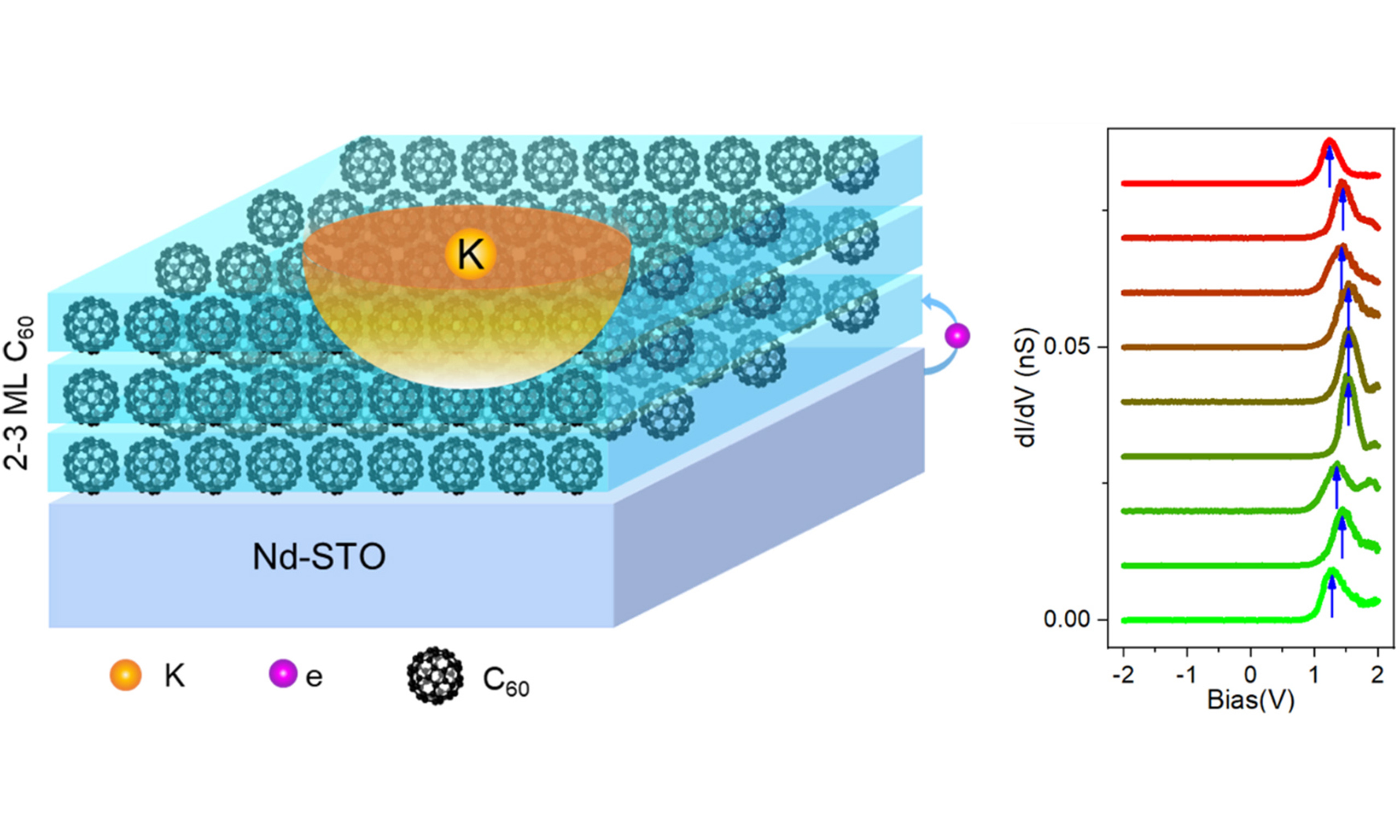
In order to provide an in-depth understanding of the charge-related phenomena in K-doped C60 layers, including charge transfer, charge trapping and band bending, we synthesized C60 multilayers on two different STO(001) clean surfaces, namely pristine and Nb (0.7 wt%)-doped STO(001) surfaces, followed by controlled K doping.
MATERIALS AND METHODS
Preparation of STO substrates
Undoped and Nb (0.7 wt%)-doped STO(001) wafers measuring 10 × 2 × 0.5 mm3 were degassed by direct current (DC) heating at 550 °C for more than 5 h in a molecular beam epitaxy (MBE) chamber. The STO wafer was heated at 800 °C for 1 h and then gradually heated up to 1,200 °C for another half an hour to obtain a TiO2-terminated STO(001) surface with 2×2 superstructure[1,30]. The superstructure was confirmed by STM observations [Supplementary Figure 1]. C60 molecules were evaporated using a Knudsen cell. The monolayer C60 film was obtained by post-annealing at 220 °C for 5 min after 5-minute deposition of C60 on the STO surface kept at room temperature (RT), while multilayer C60 films were obtained without post-annealing after 8-minute deposition. Commercial alkali metal dispensers (SAES Getters, Italy) were used and heated by a direct electric current (IK = 5.9 A) to produce potassium atoms. The pressure during the deposition of potassium atoms was maintained at around 2 × 10⁻⁹ Torr.
STM/STS measurements
All experiments were performed in a commercial ultrahigh vacuum (UHV) system (USM-1300s) consisting of a MBE chamber equipped with an insert chamber allowing in situ STM measurements at liquid-helium temperature. All STM measurements were performed in a constant current mode at 4.2 or 1 K, with a polycrystalline Pt/Ir tip and the bias voltage applied to the sample. Differential conductance (dI/dV) measurements were performed using a lock-in amplifier with a modulation frequency (f) of 271 Hz and a modulation amplitude (V) of 1-5 mV. STM images were analyzed using WsXM software[31].
Computational details
Periodic density-functional theory (DFT) calculations were performed using the Vienna Ab initio Simulation Package (version 5.4.4)[32,33]. Projector augmented wave (PAW)[34,35] pseudopotentials were employed to describe electron-ion interactions. The exchange-correlation energy of the system was described by the Perdew-Burke-Ernzerhof (PBE) functional[36]. Intermolecular forces were estimated using the vdW-D3 method developed by Grimme et al.[37]. The cutoff energy for plane waves was set at 400 eV. The convergence criterion used for atomic forces in structural optimization calculations was 0.03 eV/Å. The convergence criterion for solving the electronic wave function is a 1 × 10⁻⁵ eV energy difference. The K-point setting was based on a 1×1×1 Monkhorst-Pack grid centered at the Γ point. In this work, the simulated STM images, obtained using Hive program[38], revealed atomic-scale surface features.
The gas-phase electronic structure calculations of isolated C60 were performed using the Gaussian 16 software package (version A. 03)[39]. The geometrical structures of ground-state molecules were optimized by using the Becke three parameter Lee-Yang-Parr (B3LYP) hybrid functional combined with the 6-31G(d) basis set. Based on the optimized structures, the electronic structure of the ground-state molecule was obtained at the Becke-Lee-Yang-Parr (BLYP)/6-31G(d) level. The TiO2-surface of the SrTiO3(001) substrate was used for DFT calculation and STM simulation, as described in Ref.[39].
RESULTS AND DISCUSSIONS
Morphologies and electronic properties of undoped and 0.7 wt% Nb-doped STO(001) surface
The flat and clean terraces of both undoped and Nb (0.7 wt%)-doped STO(001) substrates have been achieved, as shown in Figure 1. On the pristine STO(001) surface, randomly distributed surface atoms appear on the surface with a corrugation approximately 200~250 pm [Figure 1A]. In contrast, surface atoms become arranged in 2×2 order on the Nb-doped STO(001) surface [Figure 1B], indicating a well-known TiO2-terminated surface. The 2×2 reconstruction is further confirmed by the 2×2 fractional spots observed in the Fourier transform image in Supplementary Figure 1B. The height profile measured on the high-resolution image of the reconstructed Nb-doped-STO surface shows that the unit cell of the surface reconstruction is about 0.8 nm, which is twice the unit cell size of the pristine SrTiO3(001) surface (~0.4 nm), consistent with a 2×2 surface reconstruction. From the dI/dV spectra acquired on both surfaces, the Nb-doped SrTiO3(001) surface shows a semiconducting gap (~2.4 eV) with a conduction band minimum (CBM) at 0.7 eV and a valence band maximum (VBM) at -1.7 eV, while the undoped SrTiO3(001) surface shows a larger gap (~3.4 eV) with a CBM at 1.1 eV and a VBM at -2.3 eV [Figure 1C]. We note that the CBM and VBM are deduced by extrapolating the rising edges of the conduction/valence bands to their respective intersection with zero. Clearly, the Nb-doped SrTiO3(001) surface exhibits a smaller semiconducting gap with partially filled conduction and valence bands, which may introduce stronger interfacial charge transfer[40,41], as demonstrated in Supplementary Figure 2 and Supplementary Table 1. The Nb-doped STO substrate can therefore provide a stronger charge transfer effect, due to interfacial oxygen vacancies[42]. Bader charge calculations in Supplementary Table 1 also show that the electron donation from STO to C60. The inclusion of both undoped and Nb-doped samples demonstrates that the Nb-doped STO substrate significantly enhances the substrate’s conductivity and ability to supply charge to adsorbed molecules, thus providing an effective method for engineering interfacial electronic properties of the C60 overlayer.
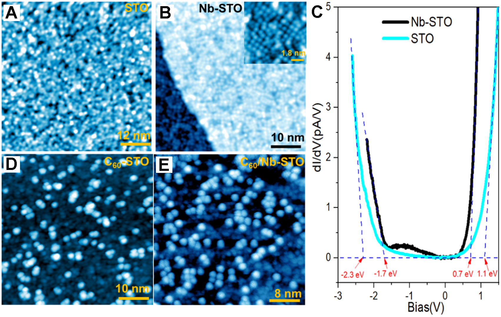
Figure 1. Images of pristine-STO and Nb-doped STO substrate and related dI/dV spectra. (A) Image of pristine STO surface (60 ×
Small point defects exist on the flat terrace [Figure 1B], which may be attributed to TiOx, a typical and unavoidable feature during thermal treatment. Such surface defects may influence the locally adsorbed C60 at short range, but have no long-range effect on the configuration and electronic properties of the C60 assembly layer. By further depositing C60 onto both undoped and Nb (0.7 wt%)-doped STO(001) surfaces with an initial coverage of about 0.3 ML, C60 molecules tended to randomly distribute as monomers on both surfaces, instead of accumulating into islands [Figure 1D and E]. With further deposition of C60, more fullerene molecules initially formed a less-ordered buffer layer, followed by the layer-by-layer growth of C60 films with self-assembled hexagonal lattices, as shown in STM images [Supplementary Figure 3]. New C60 layers formed on the existing C60 buffer layer initially nucleated in the form of trimers or tetramers, as marked by red circles in Supplementary Figure 4, indicating that the buffer layer enhances the interaction between C60 molecules and leads to a short-range ordered arrangement of C60. The existence of a buffer layer indicates that the interaction between C60 and the STO(001) substrate is relatively strong compared to the intralayer interaction within the C60 layer. Another piece of evidence for the strong interface interaction is the random adsorption of C60observed in a typical zoom-in STM topography showing the internal structure of C60 [Figure 2A].
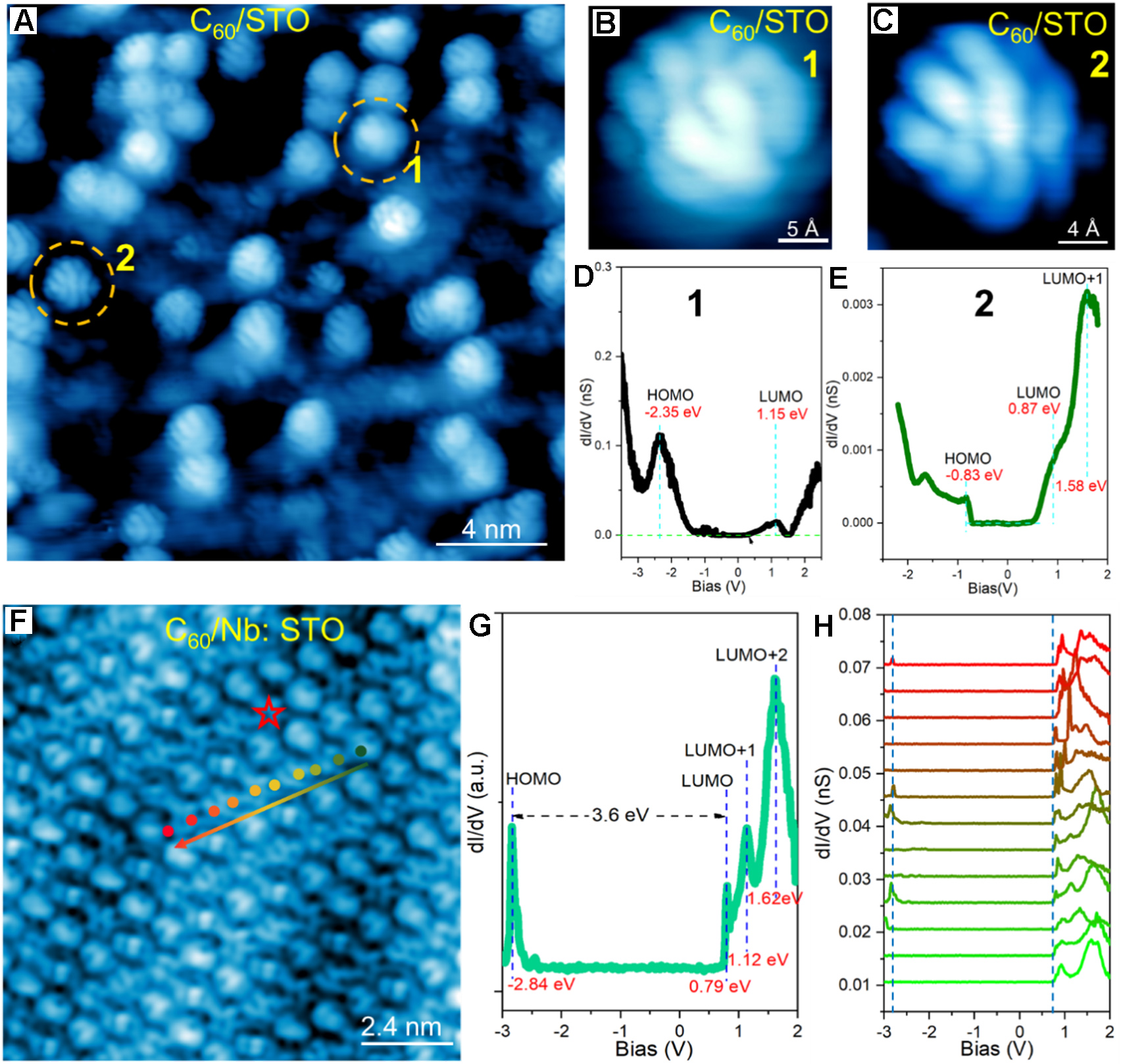
Figure 2. Topographic image and spectroscopy of C60 on undoped STO and Nb-STO substrates. (A) STM image of C60 monomers on undoped STO substrate. Image size is 20 × 20 nm2 with UB: +1.0 V and IT: 10 pA; (B and C) High-resolution image of a single C60 monomer with different internal structures. Image size is 2 × 2 nm2 with UB: +1.0 V and IT: 10 pA; (D and E) Point STS measured on top of the C60 monomer in panels (B) and (C), respectively. STS are taken by the setpoint of UB: +1.5 V, IT: 10 pA and bias modulation of 20 mV; (F) Orbital-resolved STM image of C60 monolayer on Nb-STO substrate. Image size is 12 × 12 nm2 with UB: +1.5 V and IT: 100pA; (G) STS curve measured at the location marked by red star; (H) A linear spectroscopic survey taken along the dotted line in panel (F). STS are taken by the setpoint of UB: +1.5 V, IT: 100 pA and bias modulation of 20 mV. The color gradient from green to red corresponds directly to the gradient in the (H) panel, representing the one-to-one relationship between the atomic sites in the (F) panel and the STS data in the (H) panel. All STS are taken at 4.2 K. C60: Fullerene; STO: SrTiO3; STM: scanning tunneling microscopy; STS: scanning tunneling spectroscopy; HOMO: highest occupied molecular orbital; LUMO: lowest unoccupied molecular orbital.
HOMO-LUMO gap of C60 monomers and 2D layers
By employing cryogenic scanning tunneling microscopy and spectroscopy (STM/STS), we found that fullerene molecules grow layer-by-layer after forming a relatively disordered wetting layer on the 2×2 reconstructed Nb-doped STO(001) surface. Furthermore, the monolayer of C60 shows a gap of about 3.6 eV, which is close to the reported gaps for monolayer and multilayer C60, measured to be ~4.1 and ~4.6 eV, respectively[30]. At the initial stage of C60 adsorption on the STO(001) surface, C60 molecules exist as monomers [Figure 2A]. Measured at a cryogenic temperature of 4.2 K, due to relatively strong interaction between C60 and the STO substrate, zoom-in STM images [Figure 2B and C] show the internal structure of C60, either as “fish-scale”-like [type-I, Figure 2B] or “flower”-like [type-II, Figure 2C]. Such images indicate that the C60 is partially frozen with slight rotation[43,44]. The corresponding dI/dV spectra for the two C60 configurations are shown in Figure 2D and E, respectively. The measured dI/dV curves display a small highest occupied molecular orbital (HOMO)-lowest unoccupied molecular orbital (LUMO) gap for C60 monomers, namely 3.5 eV for type I and 1.7 eV for type II, respectively. Previous work shows that the HOMO-LUMO gap of monolayer C60 on metal surfaces varies from 2.0 to 3.0 eV[4,45], while that on graphene and h-BN sheets is about 3.5 eV[17,46]. For isolated C60 in the gas phase, the difference of εLUMO - εHOMO is ~1.6 eV[15,18], which is in good agreement with our calculation [Supplementary Figure 5], and is usually assumed not to change significantly in the presence of a surface[8,47]. The enlarged HOMO-LUMO gap (ΔEgap) can be expressed as
where εLUMO - εHOMO is the molecular-orbital splitting of C60 in its ground state without considering the on-site Coulomb interaction (U)[24].
The variation in the HOMO-LUMO gap of C60 monomers depends strongly on the adsorbed configuration of C60. For type I-adsorbed C60, the molecule is mostly surrounded by other C60 molecules, resulting in stronger intermolecular coupling; therefore, the measured HOMO-LUMO gap is about 3.5 eV, close to the 3.6 eV measured for the C60 monolayer. In contrast, for the type II-adsorbed C60, the molecule is nearly isolated, and therefore the measured HOMO-LUMO gap is about 1.7 eV, close to that of an isolated C60 in the gas phase (1.6 eV).
The HOMO/LUMO gap of a C60 monomer on STO is about 1.7 eV; while the HOMO/LUMO gap of a C60 monolayer on STO is about 3.6 eV, with an uncertain contribution from the on-site U via neighboring C60 molecules [Supplementary Note 2]. When C60 molecules aggregate into a bulk or a film, U increases owing to enhanced Coulomb interaction from neighboring molecules and the substrate. Accordingly, the ΔEgap value of bulk C60 increases to 3.7 eV, as detected by photoemission spectroscopy[18].
A series of dI/dV spectra measured on the C60 layer in Figure 2F show a HOMO-LUMO gap of about 3.6 eV, as shown in Figure 2G and H. These spectra contain four distinct peaks corresponding to the HOMO, LUMO, LUMO + 1, and LUMO+2 of C60 at - 2.84, 0.79, 1.12, and 1.62 V, respectively. As seen in Figure 2H, although the HOMO energy varies with location, the LUMO energy remains unchanged, indicating enhanced Coulomb interaction for adding an electron due to neighboring molecules. As demonstrated in Supplementary Figure 6A-H, the density of states (DOS) of the C60 monolayer was calculated with various configurations. DFT calculations give a bandgap of about 3.6 eV with a DOS peak appearing inside the bandgap for all configurations. Such in-gap states could be induced by charge transfer between the C60 layer and the STO substrate, as shown in Supplementary Figures 2 and 6, and Supplementary Table 1. K-doped C60 induced a stronger charge transfer, as demonstrated by Bader charge calculations in Supplementary Table 1. More charge transfer occurs from STO to K-doped C60, leading to electron accumulation around the K dopant and trapping charge within a radius of 3 nm.
Orientational assembly of the C60 layer and effect of K-doping
Five different orientations of C60 molecules were resolved with high-resolution imaging, e.g., C-atom faced-up (CA), hexagon-pentagon bond faced-up (H:P), hexagon-hexagon bond faced-up (H:H), pentagon faced-up and deflected (P:D) and hexagon faced-up (H). The intramolecular structures of assembled C60 in the layer can be visualized using cryogenic high-resolution STM imaging, as previously demonstrated by Hou et al.[45]. Various molecular configurations were observed on the Nb-doped STO surface, as shown in Figure 3.
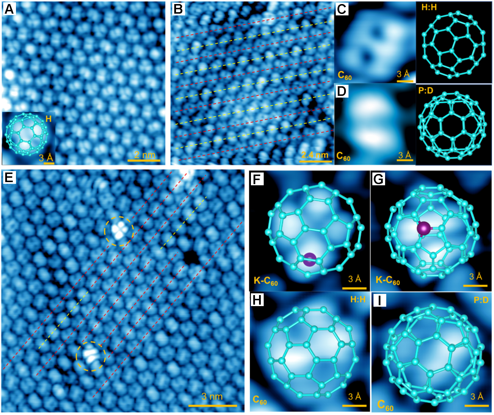
Figure 3. Topographic images of different orientational C60 assembly layers. (A) STM image of undoped C60 assembly layer showing a uniform orientation. Image size is 10 × 10 nm2 with UB: +1.0 V and IT: 150 pA. Inset: enlarged image of a single C60 molecule with a “clover”-shape, overlapped with a structure of C60 with H configuration. Image size is 1.5 × 1.5 nm2 with UB: +1.0 V and IT: 10 pA; (B) STM image of undoped C60 assembly layer showing a staggered orientation arrangement. Yellow and red dashed lines indicated two different oriented C60 chains, respectively. Image size is 12 × 12 nm2 with UB: +1.2 V and IT: 10 pA; (C and D) High resolution image showing different orbitals of C60, corresponding to two distinct orientations of C60, (“8”-shaped, H:H configuration) and (“two-lobe”, P:D configuration), respectively. [Right panels of (C) and (D)] The corresponding structure models of C60; (E) STM image of C60 layer with two K-dopants. Two bright spots, marked by orange-colored dashed circles, corresponding to two different K-doped C60. Image size is 15 × 15 nm2 with UB: +1.2 V and IT: 50 pA; (F and G) High resolution STM images of two K-doped C60, overlapped with proposed structures, (“Four leaf clover”, a K-atom embedded in a C60 with H:H configuration) and (“three-lobe”, a K-atom attached with a H:P configuration C60), respectively; (H and I) Images for two oriented C60, corresponding to the orientation of H:H configuration and hexagon facing up, respectively. Image size is 1.5 × 1.5 nm2 with UB: +1.2 V and IT: 50 pA. C60: Fullerene; STM: scanning tunneling microscopy.
Figure 3A shows a high-resolution image of a local area of the C60 layer, in which all C60 molecules exhibit a uniform configuration with a three-lobe clover-like shape, as shown in the inset figure. This image likely corresponds to the H configuration. STM imaging and simulations of C60 performed on the semiconducting CuSe monolayer seem to show a similar assignment of C60 configuration[46]. Here, in order to account for the substrate effect, we performed STM simulations for various oriented C60 on the TiO2-terminated surface of the SrTiO3(001) substrate [Supplementary Figure 7]. As shown in Supplementary Figure 7C and D, the simulated image of the H configuration displays a three-lobe shape. Figure 3B shows a high-resolution image for another local area of the C60 layer, in which C60 molecules exhibit a staggered orientational assembly. The red dashed line indicates a C60 molecule with an “8-shaped” pattern, corresponding to the H:H configuration, as shown in Figure 3C[46]. The yellow dashed line indicates a C60 molecule with a “two-lobe” internal structure, corresponding to the P:D configuration, as shown in Figure 3D[46]. However, because our simulated images do not show a clear “two-lobe” structure, we assign this feature to the P:D configuration based on Ref.[46].
However, once K is doped into a preformed C60 layer, the doped C60 molecule becomes negatively charged due to the charge transfer from K atoms[47]. This charge transfer causes the LUMO level of C60 to become partially occupied[48]. When the sample is biased at +1.4 V and above, the tunnel current is contributed by (1) direct tunneling from the STM tip to STO; and (2) tunnelling via the LUMO of C60. For a C60 molecule bonded with K, its LUMO level is partly occupied by electrons and hence it becomes more effective at conducting electrons when the sample is positively biased. This makes the doped C60 molecule appear brighter in comparison with undoped ones. Figure 3E shows a local area in the C60 layer with two prominent K-doped C60 molecules, marked by orange dashed circles. High-resolution images of two K-doped C60 molecules are shown as a “four-lobe” pattern in Figure 3F and a “three-lobe” pattern in Figure 3G, which may be assigned to a K-atom embedded in a C60 with H:H configuration and a K-atom attached to an H:P oriented C60, respectively. DFT calculations of K-doped C60 were performed and simulations of the corresponding STM images are shown in Supplementary Figure 8. In addition, DFT calculations were carried out to analyze and explain the charge density difference for various C60 configurations in Supplementary Figure 9.
Between two K-dopants, the orientation of surrounding C60 becomes more random and disordered. As shown in Figure 3E, in the area between the dopants, most C60 molecules tend to adopt the H:H configuration, while some molecules occasionally adopt the P:D configuration.
A chiral 2×2 configuration around a K-doped C60
C60 molecules tend to be either uniformly oriented or staggered in undoped C60 multilayer, and they form a chiral (2×2) superstructure in the area near the K-doped C60 dopant. In the region near a K-doped C60 molecule, Figure 4A shows a so-called chiral 2×2 superlattice. A high-resolution image of such K-doped C60 dopant [Figure 4B] shows a bright contrast with a three-lobe pattern, consistent with the proposed structural model of the configuration of “K-bond-C-atoms faced-up” (K:C) in Figure 4C. Three different C60 orientations can be observed in Figure 4A, i.e., round ball [Figure 4D], two-lobe [Figure 4E and F], and three-lobe [Figure 4G] shapes, with the latter two corresponding to the H:H and H configurations, respectively. For the C60 exhibiting the round ball shape [Figure 4D], it is well known that C60 molecules are free to rotate and flip on the surface. Therefore, the molecules do not exhibit a fixed orientation, and STM images of each molecule arise from a time-averaged signal[49]. Focusing on the three-lobe molecules with H configuration, one may identify a local 2×2 arrangement, as indicated by the yellow triangles and red rhombus in Figure 4A. A similar 2×2 superstructure originating from the partially ordered arrangement of molecular orientations has been observed in the second C60 layer grown on the STO surface[19], where H-oriented C60 molecules are well ordered, while others exhibit no long-range orientational order[50]. Our results are consistent with observations from previous work. The only difference is that the chiral 2×2 superlattice here appears to be located near a K-doped C60, rather than in the undoped C60 layer, which may be related to the enhanced charge transfer induced by K doping.
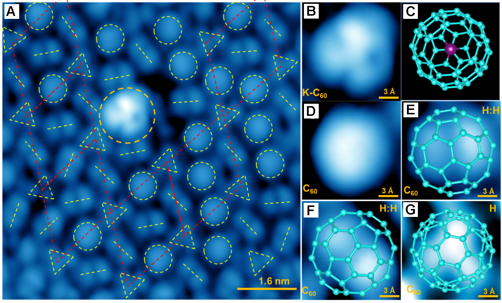
Figure 4. Topographic images of different oriented C60 assembled layers with a K-doped C60 molecule. (A) STM image of a K-doped C60 molecule surrounded by various oriented C60 molecules. Image size is 8 × 8 nm2 with UB: +1.0 V and IT: 50 pA. Yellow colored circles, dashed short lines and triangles, represent different oriented C60 molecules; (B and C) High-resolution STM image of a K-doped C60 molecule and the proposed structure with K atom replaced C and faced up; (D-G) Images of four different oriented C60, overlapped with the corresponding structure models; Image size is 1.5 × 1.5 nm2 with UB: +1.0 V and IT: 50 pA; (D) Round ball shape, suggests a rolling C60; (E and F) Two-lobe shape, suggests H:H configuration; (G) Clover shape, suggests the H configuration. The triangles are arranged in a chiral 2×2 configuration, indicated by red rhombus, as reported previously[19]. C60: Fullerene; STM: scanning tunneling microscopy.
The electronic effect of K-doping in the C60 multilayer
K-doping introduces an emergent charge-trapped state in C60 multilayer, which may be strongly related to the observed chiral (2×2) superstructure. A similar state has also been found as a charged quasiparticle formed by the coupling of excess charges (i.e., electrons or holes) with ionic vibrations from polarons in monolayer CoCl2 on highly oriented pyrolytic graphite (HOPG)[50-52]. As shown in Supplementary Figure 10, a DOS peak appears in the STS of the C60 multilayer [see Supplementary Figures 11 and 12], located at 1.85-1.9 eV for the P:D and H:H configurations [Supplementary Figure 11], while the VBM lies below the measured spectroscopic range of -3 eV. However, after K-doping, the DOS peak of the K-doped C60 molecule shifts downward to 1.54 eV [Figure 5A]. A 0.3 eV energy downshift induced by K-doping reflects electron donation from C60 molecules to the K dopant, contrary to electron donation typically observed from K atoms in the artificial Kagome framework[53]. The calculated DOS of the K-doped C60 monolayer in Supplementary Figure 6F-H shows a slightly down-shifted central peak compared to the DOS of the non-doped C60 monolayer in Supplementary Figure 6A-E, indicating an enhanced electron transfer to K-doped C60. More interestingly, an unexpected effect is revealed by a series of dI/dV spectra measured along the arrowed line crossing the K-doped C60 [Figure 5B]. Although the K-doped C60 shows a 0.3 eV downshift of LUMO, moving away from the K-doped C60, the neighboring C60 molecules show the DOS peak shifted down to 1.24 eV, namely a 0.6 eV downshift compared to the 1.85 eV peak of undoped C60 molecules.
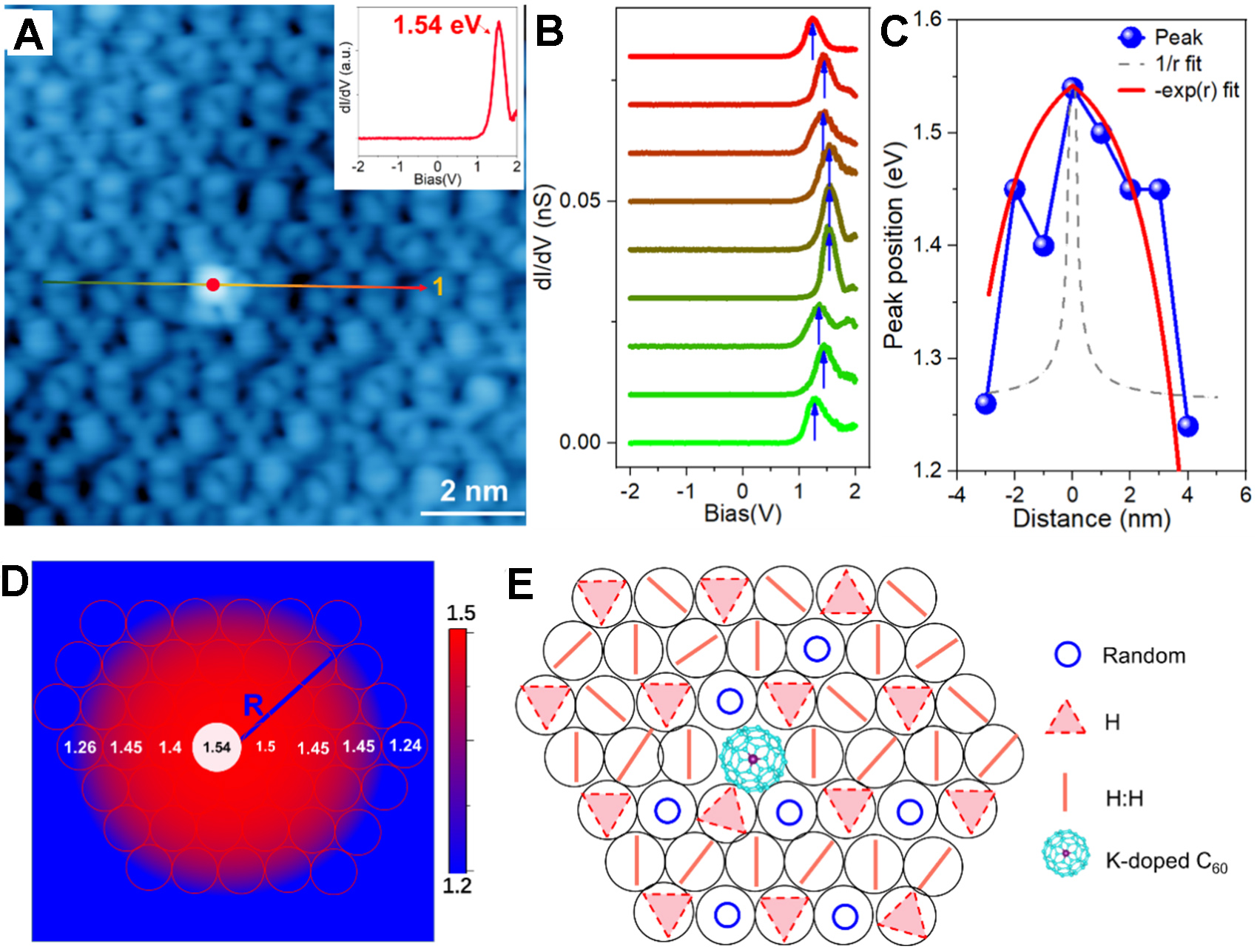
Figure 5. STS measured near K-doped C60 point defects. (A) Image of C60 layer with a point K-doped defect. (inset) dI/dV spectrum measured at the top of point defect. Image size is 10 × 10 nm2 with UB: +1.6 V and IT: 10 pA; (B) A linear STS survey measured along the colored arrowed lines in panel (A). The gradient from green to red matches the gradient color of the arrow in image (A), representing the one-to-one correspondence between the atomic sites in image (A) and the STS data in image (B). All STS measured with VB: 1.6 V, IT: 200 pA and bias modulation of 20 mV at 4.2 K; (C) Spatial dependence of peak energies measured along line STS survey (blue dots and lines). Grey dashed line is the fitting of 1/r and Red dashed line is the fitting of -exp(r), r is the distance to K-dopant; (D) Energies of peak at various spatial locations. Background is the calculated charge-trapped map based on the formula of -exp(r). R is the radius of the charge-trapped area, which is about 3 nm; (E) The orientations of each C60 molecule in layer. The circle, short bar and triangle represent the shape of round ball, two-lobe and three-lobe, respectively, corresponding to random, H:H and H configurations. The triangles (H configuration) show the quasi-(2×2) superstructure. STS: Scanning tunneling spectroscopy; C60: fullerene.
The plots for the peak energies as a function of distance to the K-dopant are shown in Figure 5C. The spatial dependence of the peak energy around the K-dopant can be expressed as Ep = -exp(r), rather than 1/r [Figure 5C], where r is the distance to the K-dopant. The peak energy variation may be due to the charge-trapped center at the K-doped site. Such a charge center induces band-bending of the CBM, where the conduction band bends upward around the charged center. This behavior may originate from the screened electric field associated with a charged center[51], suggesting that a negative charge is located at the center of the feature, consistent with the negatively charged nature of K-doped C60.
The measured peak energies with spatial location of related C60 molecules were also plotted in Figure 5D. By comparing the data with the calculated charge-trapped map based on the -exp(r) expression in the background, the radius of the charge-trapped area (R) was determined to be about 3 nm. The orientational configurations of C60 around the K-doped C60 molecule were also plotted [Figure 5E]. As seen, the three-lobe configuration (H) forms the quasi-(2×2) superstructure. The trapped charge and related (2×2) superstructure may indicate a possible mechanism of polaron formation.
Excess charge (electron or hole) trapped by self-induced lattice distortion due to electron-phonon coupling interaction (EPI) is known as a polaron[54]. Since the C60 layer is a wide-bandgap semiconductor with the bandgap of about 4.5-4.6 eV, the induced charge from K doping extends across approximately one unit cell-length of the quasi-(2×2) superstructure (> 2 nm) [Figure 5D], which is indicative of a possible polaronic nature. The polaron scenario, demonstrated in monolayer CoCl2 on HOPG[51,52], indicates a composite quasiparticle evolved from the excess carrier trapped by local lattice distortion. The polaronic state (PS) appears inside the gap and is spatially localized[52]. A significant upward bending of the conduction band near the polaron center has also been observed in monolayer CoCl2[51]. The energy downshift of the DOS peaks of K-dopant can also be attributed to the polaron formation energy, defined as the energy difference between a PS and the delocalized state at the conduction band edge[52]. Here, the polaron formation energy of K-doped C60 in the surrounding chiral 2×2 superlattice can be estimated to be about -0.3 eV at the center of the polaron (the doping site), considering the CBM at 1.85-1.9 eV. This value is comparable to the -0.24 and -0.29 eV polaron formation energies reported for Co- and Cl-centered polarons in monolayer CoCl2 on HOPG[51,52]. In our experiment, such polaron formation is also accompanied by the occurrence of a short-ranged chiral 2×2 orientational C60 assembly near the K-dopant site. Excess electrons from doped K in the C60 layer, entangled with the oriented assembly of the quasi-(2×2) superstructure, may exert significant influence on the properties of C60 layers, such as lattice reconstructions[55], carrier mobility[56,57], ferromagnetic transition[58-60], superconductivity[61-63], and other many-body correlated states[64-66].
CONCLUSIONS
In summary, the molecular orientation and electronic structure of potassium-doped C60 layers on SrTiO3(001) substrates were investigated, revealing key features such as local chiral superstructure, charge-trapped states, and conduction band bending. Fullerene multilayers were synthesized and grown on various SrTiO3(001) clean surfaces, followed by controlled K doping.
C60 molecules were found to grow layer-by-layer after forming a relatively disordered buffer layer on the SrTiO3(001) surface. An isolated C60 monomer showed a rotating orientation with a small HOMO-LUMO gap of ~1.7 eV, whereas the C60 monolayer had a wider HOMO-LUMO gap of ~3.65 eV. C60 molecules displaying different intramolecular structures were resolved using high-resolution imaging. C60 molecules tend to be uniformly oriented or staggered in undoped C60 multilayers, while forming a quasi-(2×2) superstructure near the K-doped C60 site. K-doped C60 molecules introduce a local shifting of DOS peaks and an enhanced imaging contrast, which may indicate charge-trapping effects and/or the formation of polarons. Potassium doping primarily induces a short-range, charge-trapped orientational C60 assembly near the K-dopant site and an upward bending of the conduction band due to the screened electric field of a negatively charged center. The underlying substrate acts as a template, influencing the fullerene overlayer through its geometric structure and electronic interaction at the interface. Tuning molecular orientation and electronic states in two-dimensional (2D) fullerene layers can be achieved by the cooperative effect of potassium doping and substrate selection.
These findings elucidate the profound interplay and cooperative regulation between charge, lattice, and molecular rotational degrees of freedom in such interfacial systems. This work provides new perspectives and experimental foundations for understanding and designing fullerene-based 2D functional materials.
DECLARATIONS
Authors’ contributions
Conceived and designed the experiment: Pan, M.; Chi, L.
Grew the samples: You, S.; Wang, X.; Wang, J.; Zhang, M.
Performed the STM/STS experiments: You, S.; Wang, X.; Wang, J.; Zhang, M.
Performed the DFT calculations and STM simulations: Xie, M.
Pan, M. wrote the manuscript with input from You, S., Wang, X., Wang, J., Wang, Z., Zhang, M., Xie, M., and Chi, L.
Availability of data and materials
All data analyzed to evaluate the conclusions are available within the paper and its Supplementary Materials. Further source data are available from the authors upon reasonable request.
AI and AI-assisted tools statement
Not applicable.
Financial support and sponsorship
This work was supported financially by the National Key R&D Program of China (Nos. 2022YFA1403100, 2022YFA1403101, and 2022YFA1403102), the National Natural Science Foundation of China (Nos. 22372096, 21790053, 51821002, 22072103, 22161132026, and U24A20496), the Suzhou Key Laboratory of Surface and Interface Intelligent Matter (No. SZS2022011), Gusu Innovation and Entrepreneurship Talent Program - Major Innovation Team (No. ZXD2023002), Jiangsu Excellent Postdoctoral Program (No. 2024ZB117), and the 111 Project and the China Postdoctoral Science Foundation (No. 2024M752313).
Conflicts of interest
All authors declared that there are no conflicts of interest.
Ethical approval and consent to participate
Not applicable.
Consent for publication
Not applicable.
Copyright
© The Author(s) 2026.
Supplementary Materials
REFERENCES
1. Rogero, C.; Pascual, J. I.; Gómez-herrero, J.; Baró, A. M. Resolution of site-specific bonding properties of C60 adsorbed on Au(111). J. Chem. Phys. 2002, 116, 832-6.
2. Tang, L.; Guo, Q. Orientational ordering of the second layer of C60 molecules on Au(111). Phys. Chem. Chem. Phys. 2012, 14, 3323-8.
3. David, T.; Gimzewski, J. K.; Purdie, D.; Reihl, B.; Schlittler, R. R. Epitaxial growth of C60 on Ag(110) studied by scanning tunneling microscopy and tunneling spectroscopy. Phys. Rev. B. Condens. Matter. 1994, 50, 5810-3.
4. Grobis, M.; Lu, X.; Crommie, M. F. Local electronic properties of a molecular monolayer: C60 on Ag(001). Phys. Rev. B. 2002, 66, 161408.
5. Alfonso-moro, M.; Guisset, V.; David, P.; Coraux, J.; Rougemaille, N. Describing stripelike corrugation patterns in C60 monolayers grown on Cu(111) using a frustrated spin Hamiltonian. Phys. Rev. B. 2025, 112, 054431.
6. Wang, Z.; Tao, M.; Yang, D.; et al. Strain-relief patterns and kagome lattice in self-assembled C60 thin films grown on Cd(0001). Int. J. Mol. Sci. 2021, 22.
7. Wang, Z.; Sun, K.; Tao, M.; et al. Commensurate-incommensurate transition and strain relief patterns in monolayer C60 on Cd(0001). Phys. Rev. B. 2021, 103, 245430.
8. Lu, X.; Grobis, M.; Khoo, K. H.; Louie, S. G.; Crommie, M. F. Charge transfer and screening in individual C60 molecules on metal substrates: a scanning tunneling spectroscopy and theoretical study. Phys. Rev. B. 2004, 70, 115418.
9. Cirera, B.; Liu, S.; Park, Y.; et al. Single-molecule tip-enhanced Raman spectroscopy of C60 on the Si(111)-(7×7) surface. Phys. Chem. Chem. Phys. 2024, 26, 21325-31.
10. Wang, H.; Zeng, C.; Li, Q.; et al. Scanning tunneling spectroscopy of individual C60 molecules adsorbed on Si(111)-7×7 surface. Surf. Sci. 1999, 442, L1024-8.
11. Godwin, P.; Kenny, S.; Smith, R. The bonding sites and structure of C60 on the Si(100) surface. Surf. Sci. 2003, 529, 237-46.
12. Chen, D.; Sarid, D. An STM study of C60 adsorption on Si(100)-(2×1) surfaces: from physisorption to chemisorption. Surf. Sci. 1995, 329, 206-18.
13. Ovramenko, T.; Spillebout, F.; Bocquet, F. C.; et al. STM imagery and density functional calculations of C60 fullerene adsorption on the 6H-SiC(0001)-3×3 surface. Phys. Rev. B. 2013, 87, 155421.
14. Bocquet, F. C.; Giovanelli, L.; Ksari, Y.; et al. Peculiar covalent bonding of C60/6H-SiC(0001)-(3×3) probed by photoelectron spectroscopy. J. Phys. Condens. Matter. 2018, 30, 505002.
15. Cho, J.; Smerdon, J.; Gao, L.; Süzer, O.; Guest, J. R.; Guisinger, N. P. Structural and electronic decoupling of C60 from epitaxial graphene on SiC. Nano. Lett. 2012, 12, 3018-24.
16. Jung, M.; Shin, D.; Sohn, S. D.; Kwon, S. Y.; Park, N.; Shin, H. J. Atomically resolved orientational ordering of C60 molecules on epitaxial graphene on Cu(111). Nanoscale 2014, 6, 11835-40.
17. Guo, H.; Martínez-Galera, A. J.; Gómez-Rodríguez, J. M. C60 self-orientation on hexagonal boron nitride induced by intermolecular coupling. Nanotechnology 2020, 32.
18. Ohno, T. R.; Chen, Y.; Harvey, S. E.; et al. C60 bonding and energy-level alignment on metal and semiconductor surfaces. Phys. Rev. B. Condens. Matter. 1991, 44, 13747-55.
19. Zhang, W.; Wang, X.; Liu, N.; et al. Equilibrium configurations and electronic structure of fullerene ultrathin films on SrTiO3(001) surface. Appl. Surf. Sci. 2023, 635, 157768.
20. Pandeya, R. P.; Shchukin, K. P.; Falke, Y.; et al. Molecular order induced charge transfer in a C60-topological insulator moiré heterostructure. Nano. Lett. 2025, 25, 1220-5.
21. Imada, M.; Fujimori, A.; Tokura, Y. Metal-insulator transitions. Rev. Mod. Phys. 1998, 70, 1039-263.
22. Goodenough, J. B. Electronic and ionic transport properties and other physical aspects of perovskites. Rep. Prog. Phys. 2004, 67, 1915-93.
23. Panda, S.; Das, M. K.; Mohapatra, R. R.; et al. Tuning of magnetic anisotropy and metal-insulator transition via heterointerface coupling inLaFeO3/SrRuO3 bilayers. Phys. Rev. B. 2025, 112, 054428.
24. Reyren, N.; Thiel, S.; Caviglia, A. D.; et al. Superconducting interfaces between insulating oxides. Science 2007, 317, 1196-9.
25. Umezawa, A.; Zhang, W.; Gurevich, A.; Feng, Y.; Hellstrom, E. E.; Larbalestier, D. C. Flux pinning, granularity and the irreversibility line of the high-Tc superconductor HgBa2Cu04+x. Nature 1993, 364, 129-31.
26. Jiao, X.; Dong, W.; Shi, M.; et al. Significantly enhanced superconductivity in monolayer FeSe films on SrTiO3(001) via metallic δ-doping. Natl. Sci. Rev. 2024, 11, nwad213.
27. Wang, Q.; Li, Z.; Zhang, W.; et al. Interface-induced high-temperature superconductivity in single unit-cell FeSe films on SrTiO3. Chin. Phys. Lett. 2012, 29, 037402.
28. Ren, M. Q.; Han, S.; Wang, S. Z.; et al. Direct observation of full-gap superconductivity and pseudogap in two-dimensional fullerides. Phys. Rev. Lett. 2020, 124, 187001.
29. Ahmadvand, N. Engineering C60‖B60 heterostructure for high performance electro-optic response: a theoretical performance study. Phys. Chem. Chem. Phys. 2026, 28, 2662-77.
30. Zhang, W.; Wang, J.; Wang, Z.; et al. Geometric and electronic structures of monolayer potassium fullerides on Si(111)-√3×√3-Ag. Appl. Surf. Sci. 2025, 680, 161371.
31. Horcas, I.; Fernández, R.; Gómez-Rodríguez, J. M.; Colchero, J.; Gómez-Herrero, J.; Baro, A. M. WSXM: a software for scanning probe microscopy and a tool for nanotechnology. Rev. Sci. Instrum. 2007, 78, 013705.
32. Kresse, G.; Hafner, J. Ab initio molecular dynamics for liquid metals. Phys. Rev. B. Condens. Matter. 1993, 47, 558-61.
33. Kresse, G.; Furthmüller, J. Efficient iterative schemes for ab initio total-energy calculations using a plane-wave basis set. Phys. Rev. B. Condens. Matter. 1996, 54, 11169-86.
34. Blöchl, P. E. Projector augmented-wave method. Phys. Rev. B. Condens. Matter. 1994, 50, 17953-79.
35. Kresse, G.; Joubert, D. From ultrasoft pseudopotentials to the projector augmented-wave method. Phys. Rev. B. 1999, 59, 1758-75.
36. Perdew, J. P.; Burke, K.; Ernzerhof, M. Generalized gradient approximation made simple. Phys. Rev. Lett. 1996, 77, 3865-8.
37. Grimme, S.; Antony, J.; Ehrlich, S.; Krieg, H. A consistent and accurate ab initio parametrization of density functional dispersion correction (DFT-D) for the 94 elements H-Pu. J. Chem. Phys. 2010, 132, 154104.
38. Vanpoucke, D. E. P.; Brocks, G. Formation of Pt-induced Ge atomic nanowires on Pt/Ge(001): a density functional theory study. Phys. Rev. B. 2008, 77, 241308.
39. Frisch, M.J.; Trucks, G.W.; Schlegel, H.B.; et al. Gaussian 16, Revision A.03. Gaussian, Inc., 2016.
40. Jiao, X.; Gong, G.; Zhang, Z.; et al. Post-growth Fe deposition on the superconductivity of monolayer FeSe films onSrTiO3-δ. Phys. Rev. Materials. 2022, 6, 064803.
41. Wang, L.; Ma, X.; Xue, Q. Interface high-temperature superconductivity. Supercond. Sci. Technol. 2016, 29, 123001.
42. Zhang, H.; Zhang, D.; Lu, X.; et al. Origin of charge transfer and enhanced electron-phonon coupling in single unit-cell FeSe films on SrTiO3. Nat. Commun. 2017, 8, 214.
43. Hou, J. G.; Yang, J.; Wang, H.; et al. Identifying molecular orientation of individual C60 on a Si(111)-(7×7) surface. Phys. Rev. Lett. 1999, 83, 3001-4.
44. Larsson, J. A.; Elliott, S. D.; Greer, J. C.; Repp, J.; Meyer, G.; Allenspach, R. Orientation of individual C60 molecules adsorbed on Cu(111): low-temperature scanning tunneling microscopy and density functional calculations. Phys. Rev. B. 2008, 77, 115434.
45. Hou, J. G.; Jinlong, Y.; Haiqian, W.; et al. Topology of two-dimensional C60 domains. Nature 2001, 409, 304-5.
46. Niu, G.; Geng, J.; Wang, X.; et al. Adsorption configurations and electronic properties of self-assembled C60 and C70 molecules on a semiconductor CuSe monolayer with periodic nanopores. Nanotechnology 2023, 34.
47. Lavrentiev, V.; Abe, H.; Yamamoto, S.; Naramoto, H.; Narumi, K. Isolation of Co nanoparticles by C60 molecules in co-deposited film. Mater. Lett. 2003, 57, 4093-7.
48. Matsumoto, Y.; Sakai, S.; Naramoto, H.; et al. The electronic structures of fullerene/transition-metal hybrid material. MRS. Proc. 2011, 1081, 1081-P07.
49. Nakaya, M.; Kuwahara, Y.; Aono, M.; Nakayama, T. Reversibility-controlled single molecular level chemical reaction in a C60 monolayer via ionization induced by scanning tunneling microscope. Small 2008, 4, 538-41.
50. Han, S.; Guan, M.; Song, C.; et al. Visualizing molecular orientational ordering and electronic structure in CsnC60 fulleride films. Phys. Rev. B. 2020, 101, 085413.
51. Liu, H.; Wang, A.; Zhang, P.; et al. Atomic-scale manipulation of single-polaron in a two-dimensional semiconductor. Nat. Commun. 2023, 14, 3690.
52. Cai, M.; Miao, M. P.; Liang, Y.; et al. Manipulating single excess electrons in monolayer transition metal dihalide. Nat. Commun. 2023, 14, 3691.
53. Wang, X.; Qin, T.; Ma, T.; et al. Impact of potassium doping on a two-dimensional kagome organic framework on Ag(111). J. Phys. Chem. Lett. 2025, 16, 209-14.
55. Reticcioli, M.; Setvin, M.; Hao, X.; et al. Polaron-driven surface reconstructions. Phys. Rev. X. 2017, 7, 031053.
56. Ye, Y.; Hu, Z.; Liu, J.; et al. Research progress of theoretical studies on polarons in cathode materials of lithium-ion batteries. Acta. Phys. Chim. Sin. 2020, 2011003.
57. Wang, H. M.; Liu, X. B.; Hu, S. Q.; et al. Giant acceleration of polaron transport by ultrafast laser-induced coherent phonons. Sci. Adv. 2023, 9, eadg3833.
58. Soriano, D.; Katsnelson, M. I. Magnetic polaron and antiferromagnetic-ferromagnetic transition in doped bilayer CrI3. Phys. Rev. B. 2020, 101, 041402.
59. Yan, B.; Wan, D.; Chi, X.; et al. Anatase TiO2 - a model system for large polaron transport. ACS. Appl. Mater. Interfaces. 2018, 10, 38201-8.
60. Teresa, J. M. D.; Ibarra, M. R.; Algarabel, P. A.; et al. Evidence for magnetic polarons in the magnetoresistive perovskites. Nature 1997, 386, 256-9.
61. Lim, F. H.; Ida, T.; Berciu, M. Route to phonon-mediated high-temperature unconventional superconductivity. Phys. Rev. B. 2021, 103, 064507.
62. Val’kov, V. V.; Dzebisashvili, D. M.; Korovushkin, M. M.; Barabanov, A. F. Spin-polaron concept in the theory of normal and superconducting states of cuprates. Phys.-Usp. 2021, 64, 641-70.
63. Mott, N. F. Polaron models of high-temperature superconductors. J. Phys:. Condens. Matter. 1993, 5, 3487-506.
64. Gerasimenko, Y. A.; Vaskivskyi, I.; Litskevich, M.; et al. Quantum jamming transition to a correlated electron glass in 1T-TaS2. Nat. Mater. 2019, 18, 1078-83.
65. Mostaan, N.; Goldman, N.; Grusdt, F. Unified theory of strong coupling Bose polarons: From repulsive polarons to non-Gaussian many-body bound states. Phys. Rev. Research. 2025, 7, 043349.
Cite This Article
How to Cite
Download Citation
Export Citation File:
Type of Import
Tips on Downloading Citation
Citation Manager File Format
Type of Import
Direct Import: When the Direct Import option is selected (the default state), a dialogue box will give you the option to Save or Open the downloaded citation data. Choosing Open will either launch your citation manager or give you a choice of applications with which to use the metadata. The Save option saves the file locally for later use.
Indirect Import: When the Indirect Import option is selected, the metadata is displayed and may be copied and pasted as needed.
About This Article
Copyright

Data & Comments
Data
0


Comments
Comments must be written in English. Spam, offensive content, impersonation, and private information will not be permitted. If any comment is reported and identified as inappropriate content by OAE staff, the comment will be removed without notice. If you have any queries or need any help, please contact us at [email protected].