


fig3
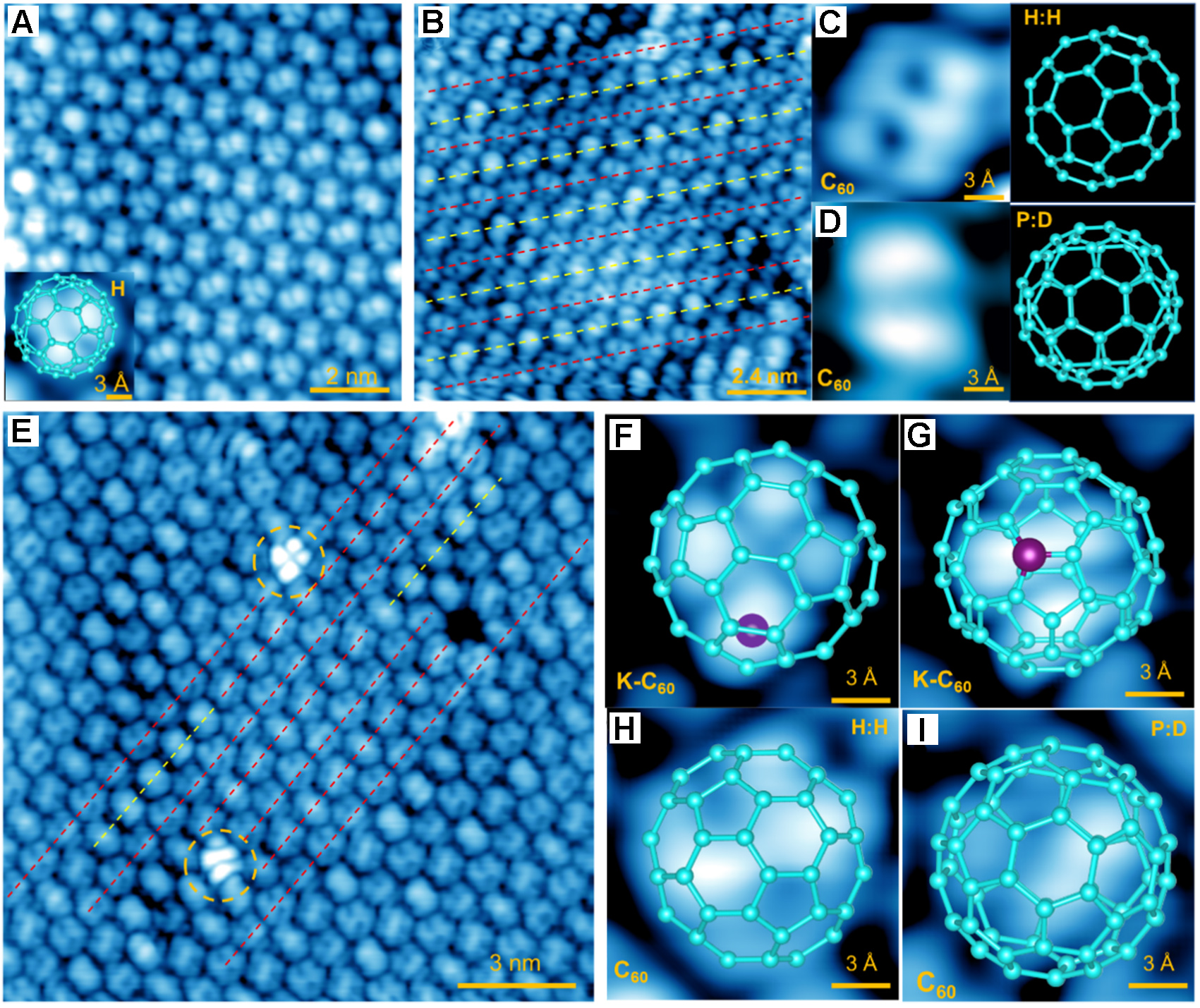
Figure 3. Topographic images of different orientational C60 assembly layers. (A) STM image of undoped C60 assembly layer showing a uniform orientation. Image size is 10 × 10 nm2 with UB: +1.0 V and IT: 150 pA. Inset: enlarged image of a single C60 molecule with a “clover”-shape, overlapped with a structure of C60 with H configuration. Image size is 1.5 × 1.5 nm2 with UB: +1.0 V and IT: 10 pA; (B) STM image of undoped C60 assembly layer showing a staggered orientation arrangement. Yellow and red dashed lines indicated two different oriented C60 chains, respectively. Image size is 12 × 12 nm2 with UB: +1.2 V and IT: 10 pA; (C and D) High resolution image showing different orbitals of C60, corresponding to two distinct orientations of C60, (“8”-shaped, H:H configuration) and (“two-lobe”, P:D configuration), respectively. [Right panels of (C) and (D)] The corresponding structure models of C60; (E) STM image of C60 layer with two K-dopants. Two bright spots, marked by orange-colored dashed circles, corresponding to two different K-doped C60. Image size is 15 × 15 nm2 with UB: +1.2 V and IT: 50 pA; (F and G) High resolution STM images of two K-doped C60, overlapped with proposed structures, (“Four leaf clover”, a K-atom embedded in a C60 with H:H configuration) and (“three-lobe”, a K-atom attached with a H:P configuration C60), respectively; (H and I) Images for two oriented C60, corresponding to the orientation of H:H configuration and hexagon facing up, respectively. Image size is 1.5 × 1.5 nm2 with UB: +1.2 V and IT: 50 pA. C60: Fullerene; STM: scanning tunneling microscopy.


