fig1

Electronic states and related orientational assembly in potassium-doped C<sub>60</sub> layer on SrTiO<sub>3</sub>(001)

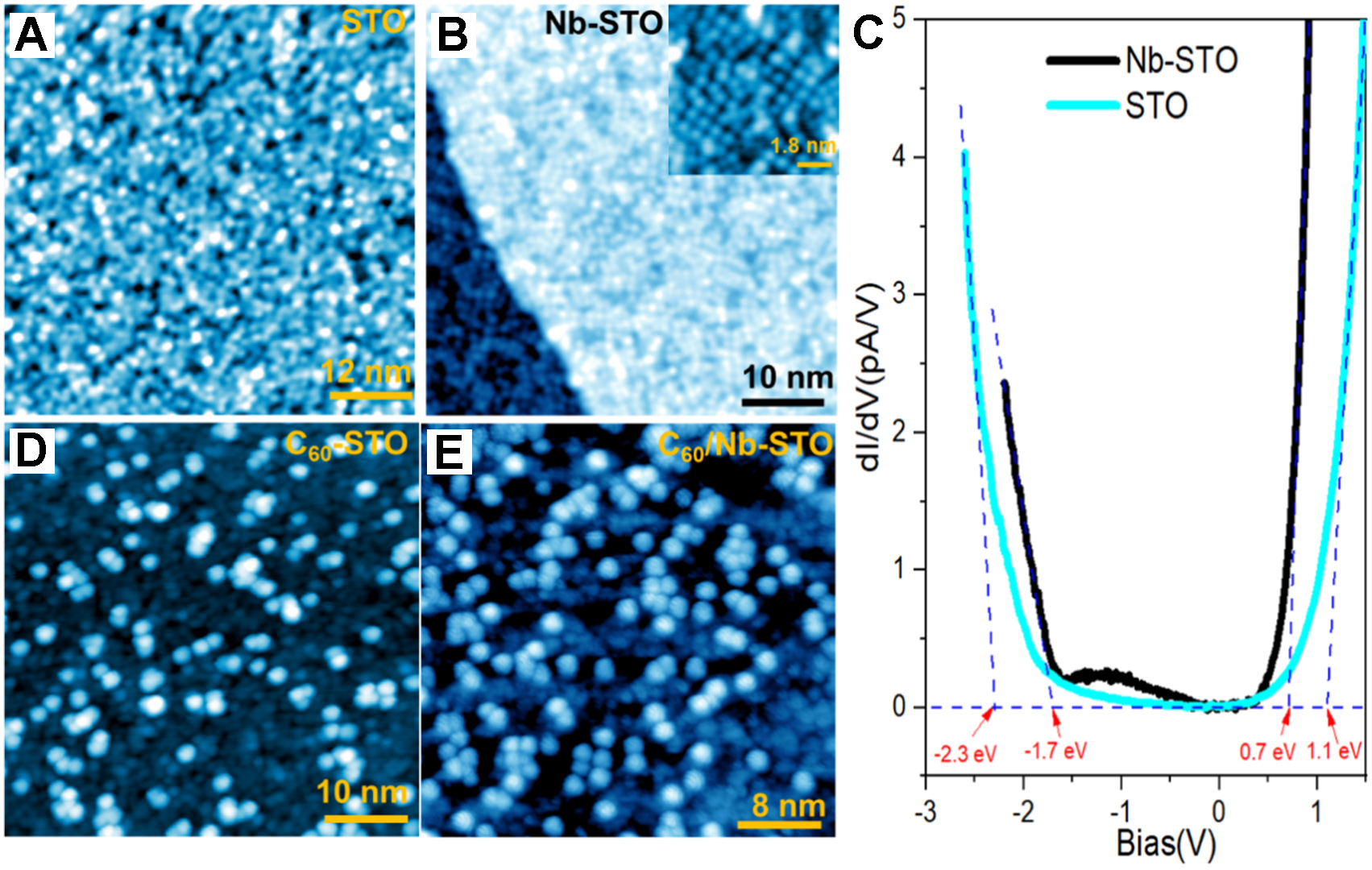
Figure 1. Images of pristine-STO and Nb-doped STO substrate and related dI/dV spectra. (A) Image of pristine STO surface (60 × 60 nm2) with UB: +1.0 V and IT: 20 pA; (B) Image of Nb-doped-STO surface (50 × 50 nm2) with UB: +1.0 V and IT: 50 pA. Inset: High resolution image of 2×2 reconstructed Nb-doped-STO surface (14 × 14 nm2); (C) dI/dV curves taken on the clean surfaces of the pristine STO (cyan) and Nb-doped STO (black) substrate, respectively. All STS measured with VB:1.2V, IT:10 pA and bias modulation of 20 mV at 4.2 K; (D) Imageof C60 deposited on the pristine STO substrate (50 × 50 nm2) with UB: +1.0 V and IT: 20 pA; (E) Image of C60 deposited on the Nb-doped STO substrate. Image size is 40 × 40 nm2 with UB: +1.0 V and IT: 20 pA. STO: SrTiO3; C60: fullerene.

Microstructures
ISSN 2770-2995 (Online)

Portico

All published articles are preserved here permanently:

https://www.portico.org/publishers/oae/

Portico

All published articles are preserved here permanently:

https://www.portico.org/publishers/oae/