


fig5
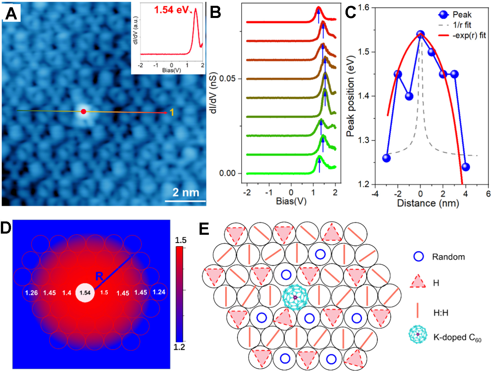
Figure 5. STS measured near K-doped C60 point defects. (A) Image of C60 layer with a point K-doped defect. (inset) dI/dV spectrum measured at the top of point defect. Image size is 10 × 10 nm2 with UB: +1.6 V and IT: 10 pA; (B) A linear STS survey measured along the colored arrowed lines in panel (A). The gradient from green to red matches the gradient color of the arrow in image (A), representing the one-to-one correspondence between the atomic sites in image (A) and the STS data in image (B). All STS measured with VB: 1.6 V, IT: 200 pA and bias modulation of 20 mV at 4.2 K; (C) Spatial dependence of peak energies measured along line STS survey (blue dots and lines). Grey dashed line is the fitting of 1/r and Red dashed line is the fitting of -exp(r), r is the distance to K-dopant; (D) Energies of peak at various spatial locations. Background is the calculated charge-trapped map based on the formula of -exp(r). R is the radius of the charge-trapped area, which is about 3 nm; (E) The orientations of each C60 molecule in layer. The circle, short bar and triangle represent the shape of round ball, two-lobe and three-lobe, respectively, corresponding to random, H:H and H configurations. The triangles (H configuration) show the quasi-(2×2) superstructure. STS: Scanning tunneling spectroscopy; C60: fullerene.


