




Regulating morphology of high-performance organic electrochemical transistors through a dual-solvent blade-coating strategy
 0
0 Abstract
Organic electrochemical transistors (OECTs) have emerged as promising candidates for bioelectronics because of their efficient ionic–electronic coupling. However, the realization of balanced ionic–electronic transport with satisfactory stability is challenging. Herein, we report a dual-solvent-assisted blade-coating strategy to modulate the morphology of hydrophilic ethylene glycol-grafted polythiophene films. The effects of the film thickness and crystallinity on OECT performance are systematically investigated. The well-ordered and uniform edge-on morphology achieved with the dual-solvent system facilitates efficient charge transport without impeding ion penetration, leading to efficient mixed ionic–electronic transport. More importantly, the operational stability is substantially enhanced compared with films processed using a single solvent, such that even thin films with thicknesses below 20 nm maintain more than 90% of their on-current after thousands of operational cycles. The optimized OECTs are successfully demonstrated for electrocardiogram (ECG) monitoring. This study provides an effective morphology engineering strategy for high-performance OECTs in wearable bioelectronics.
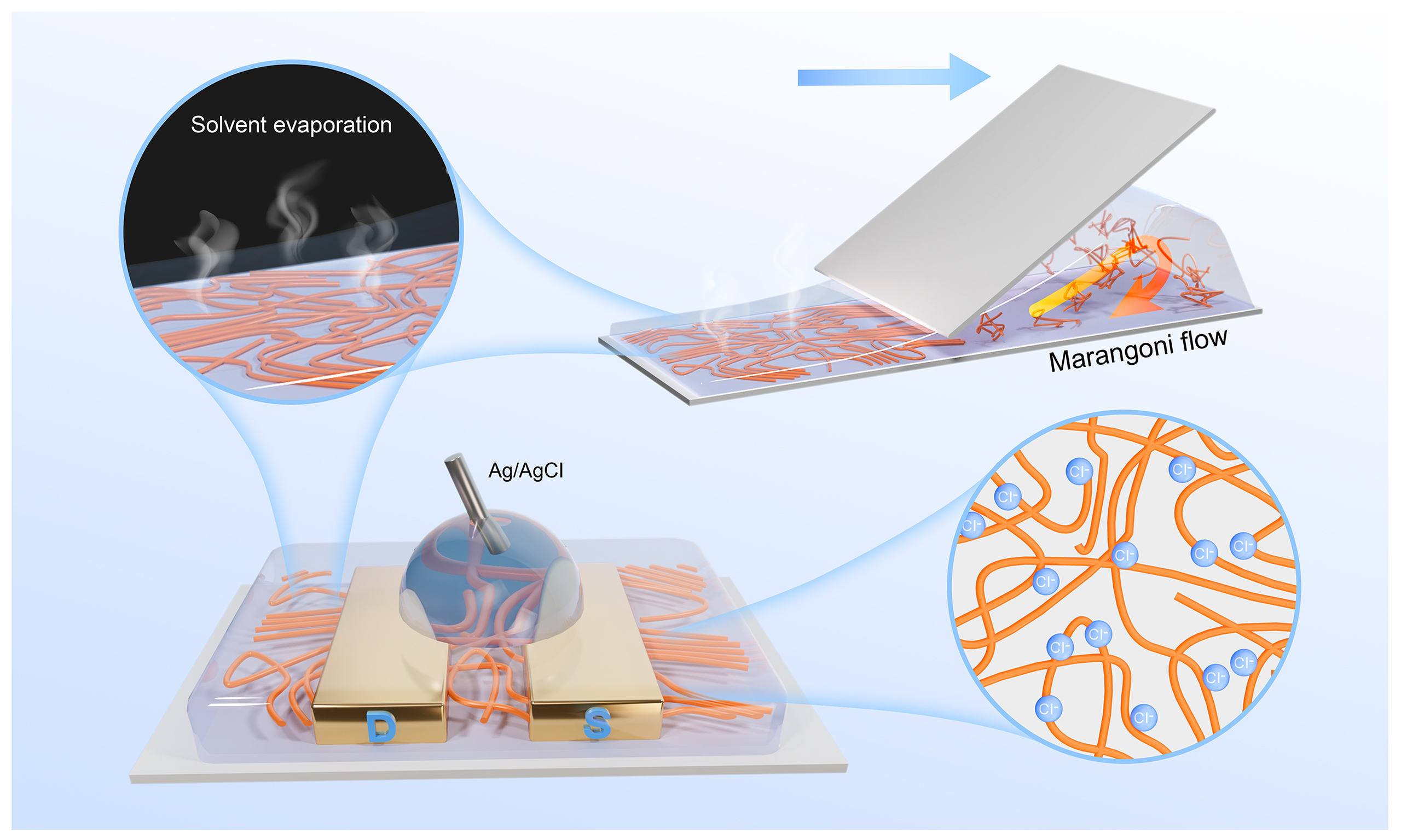
Keywords
INTRODUCTION
Organic electrochemical transistors (OECTs) have emerged as highly attractive devices in cutting-edge fields, such as flexible bioelectronics, neural interfaces, and wearable sensing, because of their remarkable ion–electron coupling capability, low operating voltage, and excellent biocompatibility[1-6]. The high performance of OECTs fundamentally relies on the efficiency of ion penetration and charge transport during the electrochemical doping process within the organic semiconductor active layer[7,8]. This efficiency depends on the intrinsic material structure and the microscopic morphology of the thin film[9-15]. While existing research has focused primarily on chemical structure modulation, a systematic and in-depth understanding of the relationship between film morphology and device performance remains lacking[16-20]. Crucially, the morphological requirements for efficient ion and charge transport present the following inherent trade-off: ion penetration depends on continuous and accessible hydrophilic or amorphous regions, whereas efficient charge transport necessitates highly ordered π–π stacking and extended crystalline domains[21-23]. Therefore, synergistically optimizing ion and charge transport through morphology engineering constitutes a central challenge in improving OECT performance. Furthermore, the film morphology is directly linked to device operational stability[24,25]. During repeated electrochemical cycling, disordered or defect-rich structures readily undergo degradation because of stress concentration induced by ion insertion/extraction. By contrast, highly crystalline and continuous network structures can effectively mitigate morphological degradation and concomitant performance decay[26-29].
In recent years, according to their primary optimization target, morphology-based strategies for improving OECT performance can be broadly categorized as follows: enhancing ionic transport or electronic transport. Ionic transport enhancement focuses on facilitating electrolyte penetration and maintaining the electrochemical doping efficiency. This strategy includes the establishment of porous or nanostructured morphologies (e.g., via humidity-induced phase separation or nanofiber networks)[30-32], additive engineering[33-35], and solvent engineering to regulate the nanoscale porosity, such as the addition of cosolvents to optimize the P-90 film morphology[36,37]. Electronic (hole) transport enhancement aims to increase charge carrier mobility by controlling crystallinity, improving molecular order via thermal annealing or molecular orientation optimization[38-41], and constructing conductive percolation networks[42]. In addition, film surface roughness constitutes a critical factor: rougher surfaces can introduce scattering centers and trap states that impede charge transport, thereby reducing mobility[12]. However, several limitations persist at the current stage. On the one hand, the synergistic optimization of both ionic and electronic transport through simple physical modulation remains challenging and often necessitates molecular design[11,22,43]. On the other hand, morphological modulation frequently neglects the structural stability of the film under repeated electrochemical cycling, resulting in performance degradation during long-term operation[44,45]. Consequently, the development of a morphology engineering strategy that can optimize both ion and charge transport pathways while ensuring high structural stability remains a key challenge. Establishing a clear relationship of morphology with mixed ionic–electronic and operation stability is also crucial.
Herein, we report a dual-solvent-mediated blade-coating method to modulate film morphology and explicitly correlate crystalline quality with ionic–electronic transport and operational stability[39,46,47]. Controlled solvent evaporation facilitates the formation of films with well-ordered edge-on packing while preserving efficient ion uptake capability, thereby achieving a balance among ionic doping, electronic transport, and operational stability. Both transconductance and operational stability are considerably enhanced compared with those of films processed with a single solvent or previously reported spin-coated films under identical geometric conditions. This improvement can be attributed mainly to the enhancement in charge carrier mobility and mechanical stability due to the uniform and highly ordered morphology. This study provides valuable insights into process optimization for high-performance OECTs and advances the understanding of morphology–performance relationships.
EXPERIMENTAL
Materials and film preparation
Poly[3,3′-bis[2-[2-(2-methoxyethoxy)ethoxy]ethoxy]-2,2′:5′,2′′-terthiophene-5,5′′-diyl] [P(g2T-T)] [molecular weight (Mw) > 10 kDa; polydispersity index (PDI) < 3] was purchased from Derthon Optoelectronics Materials. Chloroform (purity > 99%) was sourced from Sinopharm Chemical Reagent Co., Ltd., and acetonitrile (purity > 99%) was acquired from Aladdin. P(g2T-T) was dissolved at a concentration of 6 mg/mL in pure chloroform or a blended solution comprising 85% chloroform and 15% acetonitrile. The solution was stirred at 60 °C and 1,100 rpm for 2 h. Finally, thin films were prepared using a custom-built blade-coating instrument at rates of 0.3, 0.6, 0.9, 1.8, 3.0 and 6.0 mm/s. The nominal blade-coating parameters included a blade height of 0.2 mm and a substrate temperature of 30 °C.
Device fabrication
Bottom-contact transistor devices were fabricated on heavily doped silicon substrates with a 300-nm thermally grown SiO2 layer (Si/SiO2). The substrates were cleaned through sequential ultrasonication in acetone, ethanol, and deionized water, with each step lasting 10 min at room temperature. Photolithography followed by electron-beam deposition was employed to pattern source and drain electrodes (3-nm Cr and 40-nm Au electrodes, respectively; purity: 99.99%) on the Si/SiO2 substrates, with a deposition rate of 0.3 Å·s-1 to ensure high-quality films. After peeling, the patterned substrate is ready for blade coating. A similar procedure was employed for devices fabricated on polyethylene naphthalate (PEN) substrates.
Characterization and testing
OECT measurements: OECT measurements were conducted using a semiconductor parameter analyzer (model JJS-BE-150; Primarius Technologies Co., Ltd., China). All measurements were performed using Ag/AgCl pellet gate electrodes. A KCl solution (0.1 M) was added on top of the OECTs as the electrolyte. All transfer measurements were conducted at a scan rate of 20 mV/s. All the devices were tested at least 3 times.
Atomic force microscopy (AFM) and grazing incidence wide-angle X-ray scattering (GIWAXS) characterization: AFM images were obtained using a Bruker Dimension Icon atomic force microscope (Bruker, USA) operating in tapping mode with a silicon probe (model OETSPA-R3; cantilever spring constant: 40 N·m-1). Two-dimensional grazing incidence wide-angle X-ray scattering (2D-GIWAXS) measurements were performed at beamline BL14B1 of the Shanghai Synchrotron Radiation Facility (SSRF, China). The incidence angle was 0.12°, and the exposure time was 50 s. Samples were prepared on SiO2 substrates.
Electrochemical impedance spectroscopy (EIS): EIS was performed using an SP-150e potentiostat (Bio-Logic SAS, France) with EC-Lab software. The sample preparation process involved coating the polymer materials (all at a concentration of 6 mg/mL) onto indium tin oxide (ITO) substrates. Measurements were conducted in a 0.1 M KCl solution using an EC-Lab device by applying a direct current (DC) offset of 1 V with small
Ultraviolet–visible (UV–Vis)-NIR absorption: UV–Vis spectra were recorded on a PerkinElmer Lambda 950 instrument (USA). All the polymer solutions were prepared at a concentration of 6 mg/mL. Films were prepared through spin-coating on ITO substrates. In the testing process, the films were immersed in a 0.1 M KCl solution, and the measurement wavelengths ranged from 300 to 1,000 nm.
Electrocardiogram (ECG) testing: In ECG signal recording, commercially available disposable ECG electrodes supplied by Kangshi Medical Devices Co., Ltd., were used and coated with medical conductive paste to ensure effective contact with human skin. This noninvasive procedure posed no risk or discomfort to the participants and was approved by the Ethics Committee of Soochow University (SUDA20250609H08). The electrodes were connected to the source and gate of the OECT device to ensure the collection of ECG signals through the gate voltage. Measurements and recordings were made using JJS-BE-150 and FS-ProWS instruments, respectively, from Primarius Technologies Co., Ltd., China.
RESULTS AND DISCUSSION
Film morphology and structure
The molecular structure of P(g2T-T) and a schematic image of blade coating are shown in Figure 1A and B, respectively. For the single-solvent system, typical chloroform was adopted, while for the dual-solvent system, chloroform with 15% acetonitrile was selected. The choice of acetonitrile as the second solvent lies in its relatively high boiling point, high polarity, and high surface tension, which can induce solution aggregation and extend the drying window for ensuring ordered packing. To compare morphologies, we initially characterized P(g2T-T) films processed using single- (chloroform) and dual-solvent systems (chloroform:acetonitrile = 85%:15%) through AFM. As shown in Figure 1C-F and Supplementary Figure 1, the films processed with the single-solvent system (pure chloroform) were fibrous and exhibited a porous structure. When the blade-coating speed was increased from 0.3 to 6.0 mm/s, the film uniformity, thickness, and surface roughness notably changed. At low shear speeds (0.3-0.6 mm/s), relatively nonuniform films with wrinkled structures were obtained [Supplementary Figure 2A]. As the speed was increased to approximately 0.9-3.0 mm/s [Supplementary Figure 2B-D], the solvent evaporation rate achieved a balance with the coating speed, and the produced film became relatively uniform and dense[48-51]. With increasing shear speed, the surface roughness first decreased from 2.26 to 0.72 nm but then increased to more than
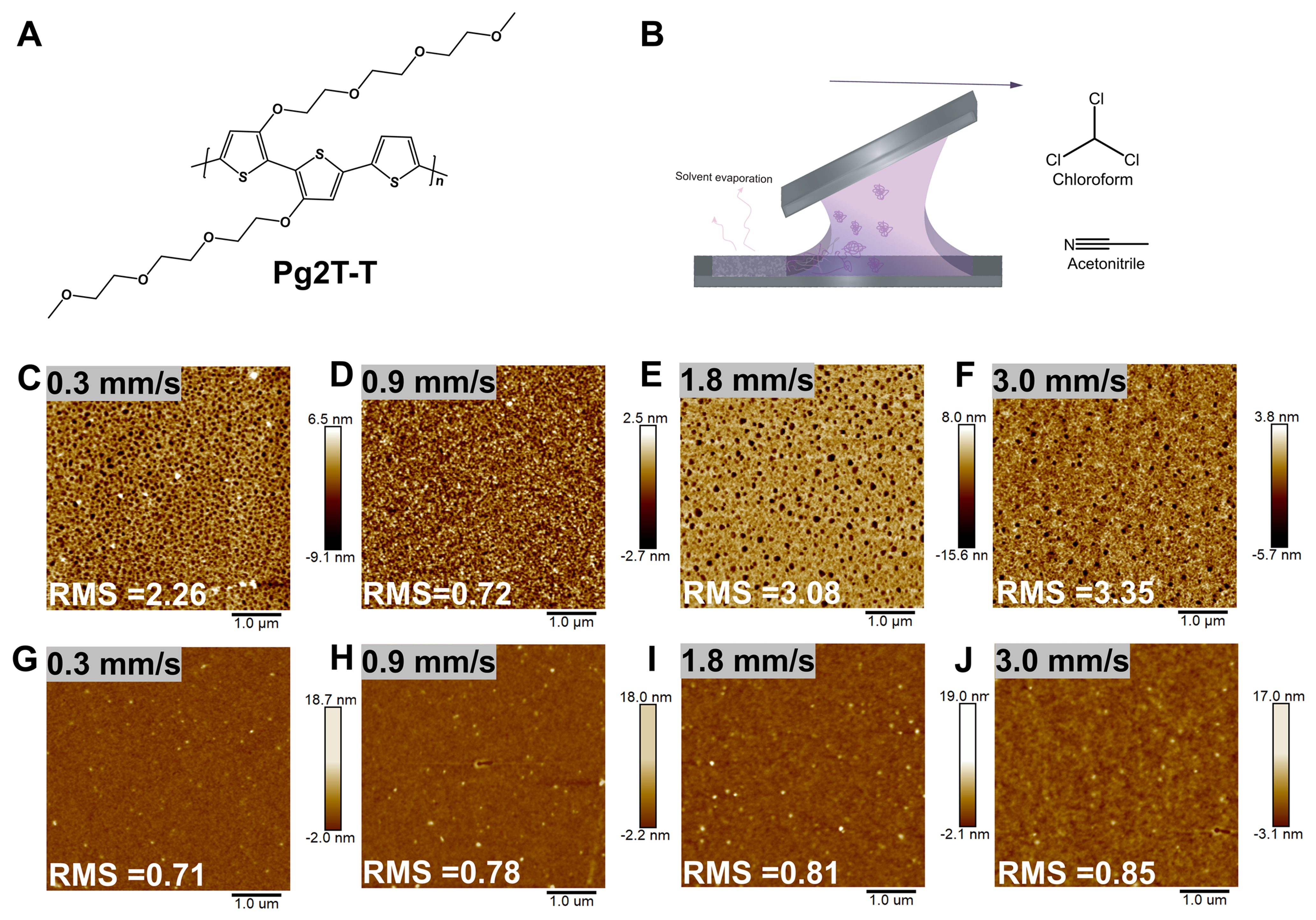
Figure 1. (A) Chemical structure of P(g2T-T); (B) Schematic diagram of blade coating; (C-F) AFM height images of single-solvent system-processed blade-coating films at rates of (C) 0.3 mm/s, (D) 0.9 mm/s, (E) 1.8 mm/s, and (F) 3.0 mm/s; (G-J) AFM height images of dual-solvent system-processed blade-coating films at rates of (G) 0.3 mm/s, (H) 0.9 mm/s, (I) 1.8 mm/s, and (J) 3.0 mm/s. P(g2T-T): Poly[3,3′-bis[2-[2-(2-methoxyethoxy)ethoxy]ethoxy]-2,2′:5′,2′′-terthiophene-5,5′′-diyl]; AFM: atomic force microscopy; RMS: root mean square.
To evaluate the quality of thin films, 2D-GIWAXS measurements were conducted. The GIWAXS patterns of films fabricated using single- and dual-solvent systems under varying coating speeds are shown in Figure 2A-H. All the patterns exhibited distinct out-of-plane (qz) diffraction signals corresponding to the (00l) plane, indicating a predominant edge-on molecular orientation with the polymer backbone aligned parallel to the substrate. Notably, compared with those processed with the single-solvent system, the films processed with the dual-solvent system exhibited greater diffraction, as indicated by the more intense (001) diffraction spots and the emergence of well-ordered reflections from the (002) and (003) planes. The direct comparisons in Figure 2I-L revealed that the diffraction signal intensity for the (001) plane was obviously higher for the dual-solvent system-processed film than for the single-solvent system-processed film, demonstrating greater crystallinity for the dual-solvent system at an identical coating speed. The calculated lamellar spacing distance of the films processed with the single-solvent system was 14.87 Å, which was slightly shorter than that of the films processed with the dual-solvent system (14.96 Å) at speeds greater than 0.6 mm/s. These values were lower than that of the spin-coated film (spacing = 17.2 Å)[21]. These lower values can be attributed to the slow evaporation and controlled assembly during shear processing, which allow more uniform and dense edge-on packing. At a low shear rate (0.3 mm/s) with the single-solvent system, the lamellar spacing became similar to that of the spin-coated film. Overall, the results suggest that dual-solvent system processing produces films with greater uniformity and better molecular assembly structures, which may facilitate charge carrier transport.
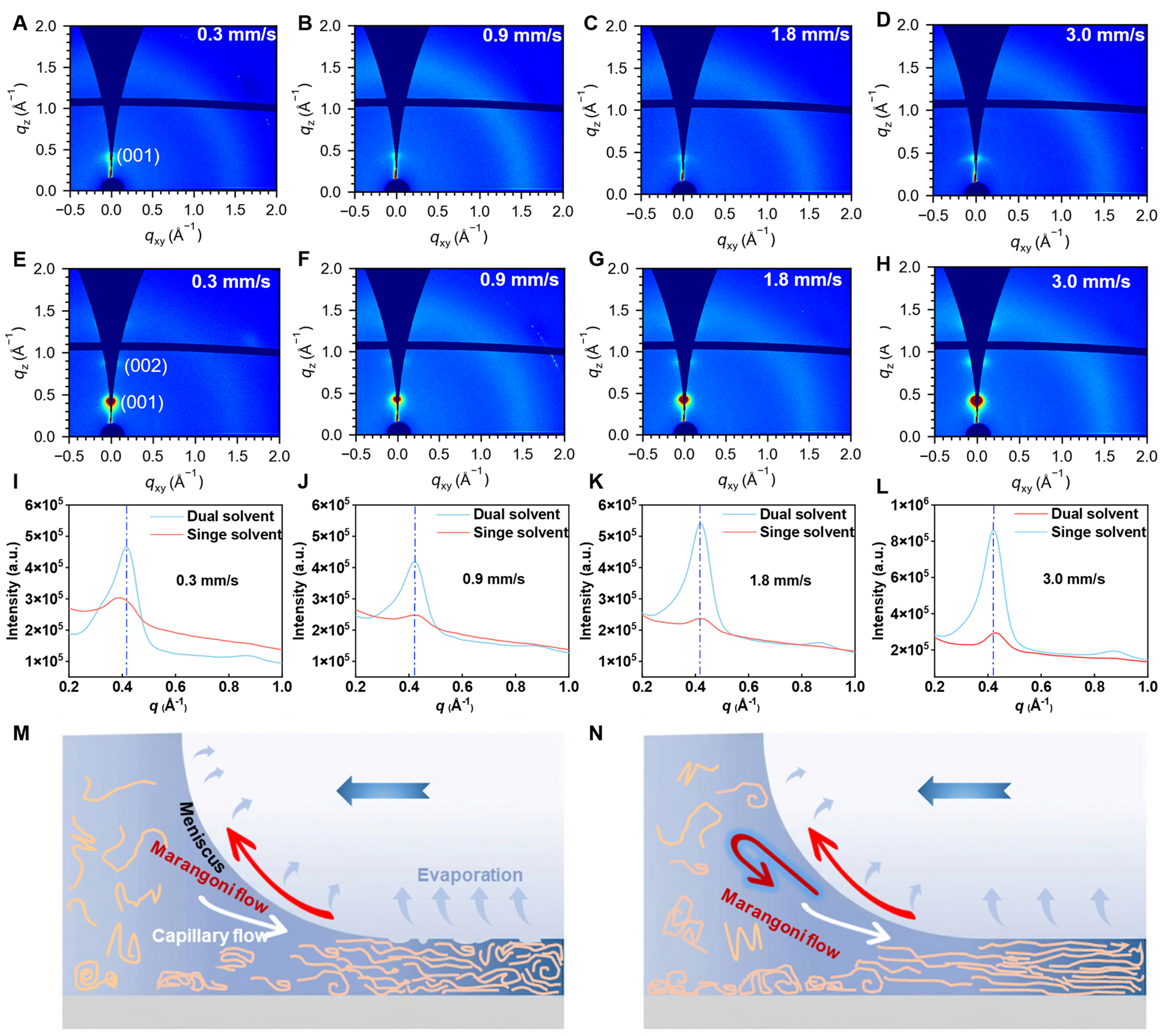
Figure 2. (A-D) GIWAXS characterization of thin-film samples processed with a single-solvent system at speeds of 0.3, 0.9, 1.8 and
According to previous reports[52,53], during solution processing of organic semiconductor films, single-solvent systems suffer from rapid evaporation of the solvent, which induces intense outward capillary flow. This flow drives solute transport toward the contact line, causes premature freezing of polymer chains, and produces a notable coffee-ring effect, ultimately yielding rough, defect-rich films with low crystallinity[54-56]. By contrast, dual-solvent systems with a high-boiling component, such as the acetonitrile employed herein, can extend the effective drying time and simultaneously establish a persistent surface tension gradient, thereby enhancing Marangoni backflow, which counteracts the outward capillary flow. The resulting balance of internal flow fields, combined with a more moderate evaporation rate, effectively suppresses uncontrolled edge accumulation of the solute and provides polymer chains with sufficient time to relax and reorganize[57-59]. Consequently, ordered interfacial self-assembly and π–π stacking are promoted, leading to the formation of large-area, continuous, and dense films with high crystallinity[15,60,61]. The different mechanisms of film formation are shown in Figure 2M and N.
To elucidate the electrochemical doping process of the films obtained under these two processing conditions, we characterized the UV–Vis–NIR absorption spectra of the dry film and 0.1 M KCl electrolyte under various bias voltages, as shown in Supplementary Figure 4. The absorption of the dry P(g2T-T) film was centered primarily between approximately 600 and 700 nm, with peaks at approximately 620 and 670 nm
OECT performance
To evaluate the electrochemical properties of films formed using the two solvent systems, OECT devices with the structure shown in Figure 3A were fabricated across a range of blade-coating speeds. Ag/AgCl pellets were employed as the gate, and 0.1 M KCl was adopted as the electrolyte. At least 3 batches of 10 independent devices were manufactured and measured under each condition, with a yield rate greater than 85%, thereby ensuring the repeatability of electrical characteristics (the error bars in the figure indicate the standard deviation of multiple devices).
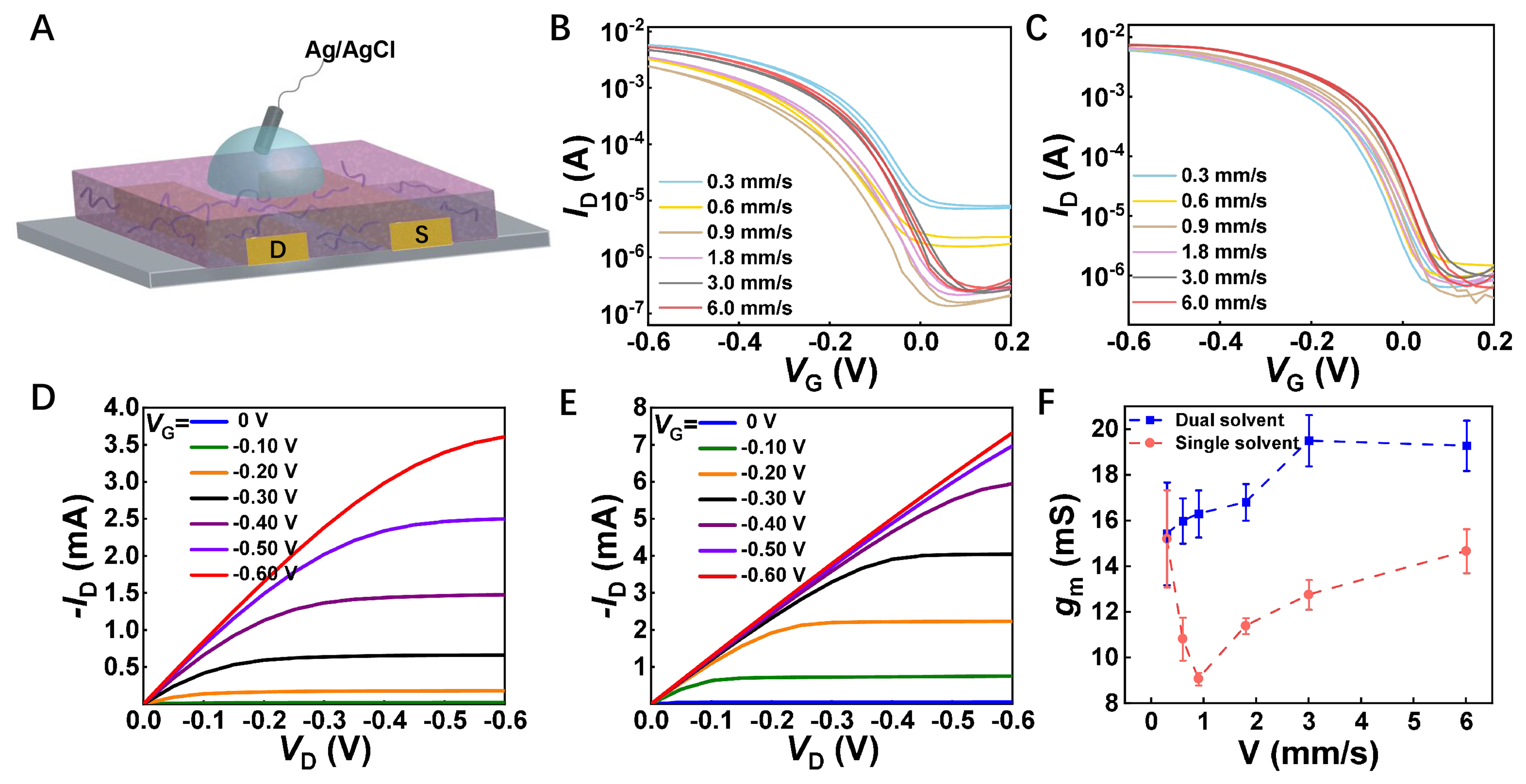
Figure 3. (A) Schematic illustration of the device structure; (B) Transfer curves for films formed with the single-solvent system at different coating speeds; (C) Transfer curves for films formed with the dual-solvent system at different coating speeds; (D) Output curve of the film formed with the single-solvent system at a velocity of 1.8 mm/s; (E) Output curve of the film formed with the dual-solvent system at a velocity of 1.8 mm/s; (F) Comparison of peak transconductance between the single- and dual-solvent devices at different blade-coating speeds. The error bars indicate the standard deviation (each point represents n ≥ 10 independent devices). The channel width (W) is
The transfer characteristics of devices obtained with both single- and dual-solvent systems at speeds ranging from 0.3 to 6.0 mm/s are shown in Figure 3B and C. The devices obtained with the dual-solvent system demonstrated higher drain currents at the same speed, suggesting better performance. Moreover, compared with the single-solvent devices (VG, peak = -0.44~-0.60 V; Table 1), the dual-solvent devices reached peak transconductance at a lower gate voltage (VG, peak = -0.35~-0.42 V). Typical output curves at a speed of
Electrical properties of the OECTs (W = 1,340 µm; L = 10 µm) obtained through single- and dual-solvent system processing at different shear rates
| Solvent | V (mm/s) | d (nm) | gm, p (mS) | µC* (F·cm-1·V-1·s-1) | C* (F·cm-3) | µ (cm2·V-1·s-1) | V G, peak (V) |
| Single solvent | 0.3 | 55 ± 5 | 15.21 ± 1.12 | 47.99 ± 3.40 | 204.50 | 0.23 | -0.44 |
| 0.6 | 13 ± 2 | 10.83 ± 0.94 | 135.15 ± 10.50 | 200.00 | 0.67 | -0.60 | |
| 0.9 | 7.5 ± 2 | 9.08 ± 0.55 | 151.76 ± 6.40 | 173.90 | 0.87 | -0.60 | |
| 1.8 | 16 ± 3 | 11.40 ± 0.56 | 130.88 ± 5.50 | 233.80 | 0.56 | -0.56 | |
| 3.0 | 25 ± 3 | 12.76 ± 0.75 | 103.5 ± 6.80 | 238.70 | 0.43 | -0.48 | |
| 6.0 | 48 ± 3 | 14.67 ± 0.96 | 49.58 ± 4.30 | 201.80 | 0.25 | -0.46 | |
| Dual solvent | 0.3 | 27 ± 2 | 15.43 ± 2.25 | 110.12 ± 5.34 | 220.78 | 0.50 | -0.42 |
| 0.6 | 16 ± 2 | 15.99 ± 0.99 | 182.9 ± 8.66 | 174.74 | 1.05 | -0.42 | |
| 0.9 | 20 ± 2 | 16.30 ± 1.03 | 160.39 ± 5.45 | 236.20 | 0.68 | -0.38 | |
| 1.8 | 25 ± 3 | 16.81 ± 1.30 | 137.48 ± 7.44 | 321.76 | 0.43 | -0.40 | |
| 3.0 | 48 ± 4 | 19.50 ± 0.52 | 94.07 ± 6.09 | 238.98 | 0.39 | -0.36 | |
| 6.0 | 58 ± 4 | 19.28 ± 1.32 | 50.42 ± 4.89 | 174.11 | 0.29 | -0.35 |
where gm is the transconductance (mS), W is the channel width (μm), d is the thickness of the active layer (nm), L is the channel length (μm), μ is the charge-carrier mobility (cm2·V-1·s-1), C* is the volumetric capacitance (F·cm-3), VT is the threshold voltage (V), and VG is the gate voltage (V).
According to Figure 3F, gm tends to saturate when the thickness is > 50 nm. Several previous reports have demonstrated geometry-dependent performance, particularly for interdigital electrodes. For a clear performance comparison, we also fabricated devices with W = 100 μm and L = 10 μm, which are typically employed by researchers [Supplementary Table 1]. The peak transconductance values ranged from 9.73 to 12.61 mS for the dual-solvent approach, which were higher than those for the single-solvent devices. The normalized transconductance of the 48-nm film (3.0 mm/s) reached 263 S·cm-1 for our devices, which also outperformed reported P(g2T-T) OECTs with similar geometries (refer to Supplementary Figure 5 and Supplementary Table 2 for details), suggesting satisfactory mixed ionic–electronic performance of the dual-solvent films.
Furthermore, the μC* product was extracted from the transfer curves according to Equation (1). With this method, thinner films typically achieved higher μC* values. Nevertheless, under a similar thickness range (d < 40 nm), the μC* values of the dual-solvent devices were approximately 30% greater than those of their single-solvent counterparts. A reduced μC* was observed at a larger thickness. To more objectively assess the differences in μC*, we also measured the peak transconductance of a series of devices with varying W and d values and extracted μC* values using the linear fitting method, as shown in Supplementary Figure 6. The extracted μC* reached 117.2 F·cm-1·V-1·s-1 for the dual-solvent system, which was greater than that for the single-solvent system (77.1 F·cm-1·V-1·s-1) and comparable to that of high-performance OECTs.
To better understand the difference between the ion and electron transport abilities of the dual-solvent films, we extracted the volumetric capacitance (C*) through EIS characterization (details are shown in Supplementary Figures 7 and 8) and subsequently calculated the charge carrier mobility (μ) using µC*/C*, as summarized in Table 1. The C* values ranged mainly from 174 to 240 F·cm-3 for single-solvent devices, whereas the values ranged from 174 to 321 F·cm-3 for dual-solvent devices as the coating speed varied, suggesting that the two types of films exhibit similar ion-doping capabilities. However, the calculated mobility values ranged from 0.23 to 0.87 cm2·V-1·s-1 for single-solvent devices but ranged from 0.29 to
As discussed above, the strong correlation between the blade-coating speed and the film thickness indicates that the performance comparisons at different rates do not fully isolate the thickness factor. To better understand the performance differences resulting from the two processing conditions, we systematically compared key OECT electrical parameters for P(g2T-T) films obtained using the single- and dual-solvent systems at identical average thicknesses (16, 25, and 48 nm). Comparisons of gm, p, gm, n, µC*, µ and C* are shown in Figure 4A-E. The analysis results demonstrated that the dual-solvent strategy delivers a consistent and significant increase in performance across all thicknesses (Student’s t test, P < 0.05). The peak gm value increased by approximately 1-fold, from ~11 to ~19 mS. Notably, the normalized transconductance of the 16-nm dual-solvent film reached a high value of 640 S·cm-1 (W/L = 10), surpassing previously reported values[4,11,21,31]. This high gm value of thinner films can be attributed to the higher effective gate potential and more uniform ion doping[23,62-64]. Furthermore, at the same thickness, the figure of merit (µC*) was consistently greater for the dual-solvent films. While the volumetric capacitance C* values remained similar, the charge carrier mobility (µ) notably improved in the dual-solvent films. Hence, the main reason for the higher mixed ionic–electronic transport performance of the dual-solvent films lies in the improved charge transport, which originates from the uniform edge-on ordering of the films.
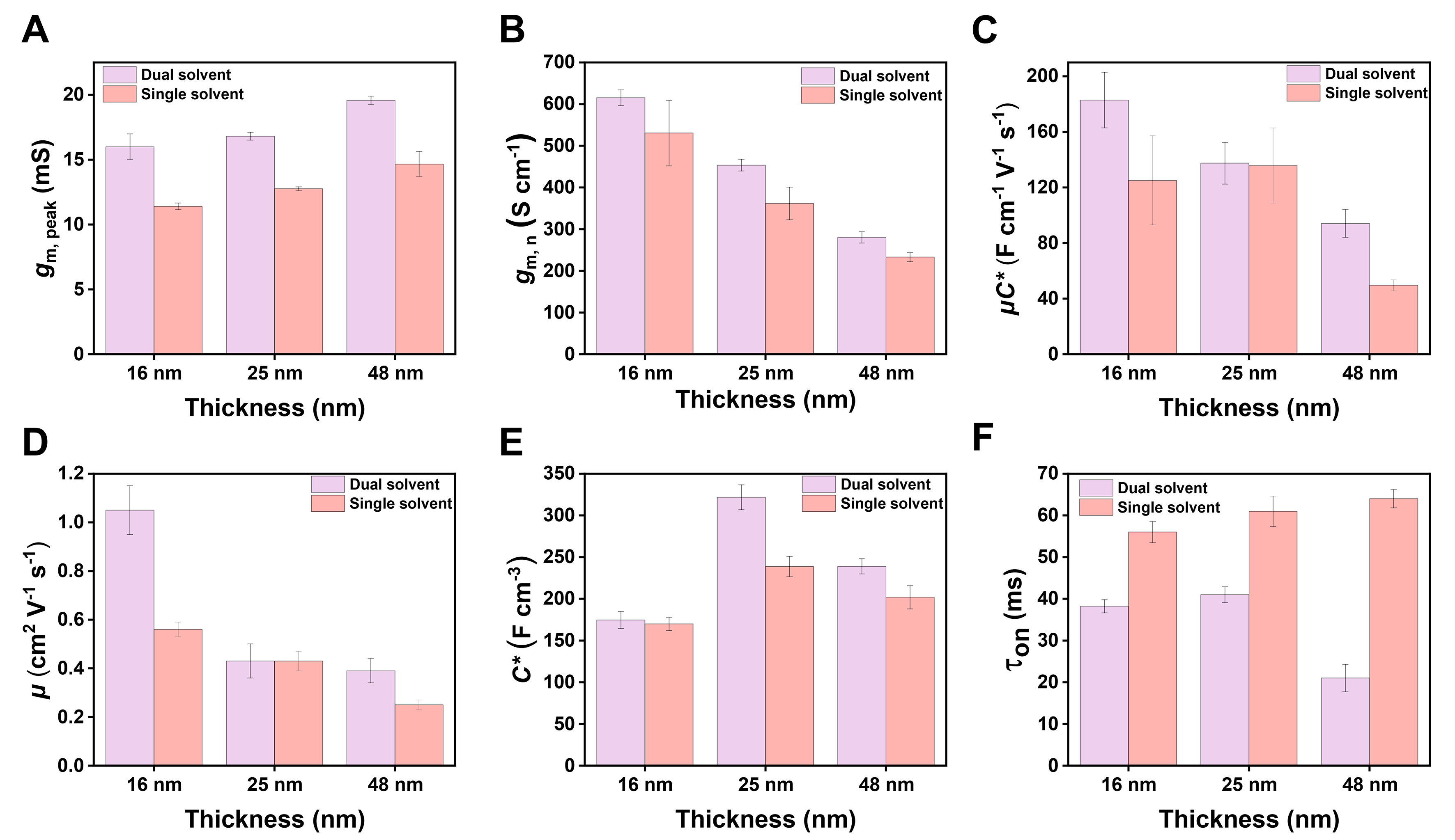
Figure 4. Comparison of the performance levels of single/dual-solvent devices at the same thicknesses of 16, 25, and 48 nm: (A) Peak transconductance; (B) Normalized transconductance; (C) Quality factor µC*; (D) Carrier mobility; (E) Volumetric capacitance; (F) Turn-on time. The error bars indicate the standard deviation (n ≥ 10 independent devices).
The dynamic response was also analyzed, and the device turn-on times (the time at which 90% of the peak current is reached during switching on) were compared (Supplementary Figure 9 and Figure 4F, respectively). With respect to the single-solvent system, thinner films were turned on faster[65-68], as expected. Intriguingly, with respect to the dual-solvent system, all the films demonstrated slightly faster on-switching under identical thicknesses, indicating that efficient ion uptake and doping capabilities are maintained. Crucially, ion transport channels do not severely compromise charge transport pathways, thereby maximizing the efficiency and speed of ion transport within the channels. This result confirms that for an identical ion penetration distance, ions penetrate and are transported faster within the dual-solvent film, which is a direct consequence of its morphologically optimized structure achieved through modified solvent kinetics.
Generally, according to the performance and key parameters comparison results, the dual-solvent treatment yields increased µ values without compromising C*. This finding is closely related to the morphology and packing of the films. The uniform edge-on orientation together with the better/smooth crystallinity of the dual-solvent films contributes to enhanced charge transport, while the films can still maintain fast ion doping, thus enabling efficient mixed ionic–electronic transport performance.
Operational stability
Beyond static electrical performance, operational stability is another critical metric for assessing the viability of OECTs in long-term monitoring-related applications. We systematically investigated the stability of P(g2T-T) films of identical thicknesses prepared with the single- and dual-solvent systems after 5,000 consecutive switching cycles in 0.1 M KCl electrolyte. The stability of the 16-, 25-, and 48-nm films during cycling is shown in Figure 5A-F, where the gate voltage was swept from 0.2 to -0.6 V over each cycle. The results revealed a stark contrast in stability behavior. Notably, the stability of the dual-solvent films significantly increased across the tested thickness range (Student’s t test, P < 0.05). With respect to single-solvent devices, the stability greatly depends on their thickness: thinner films are more severely degraded. After nearly 3 h of repeated cycling, the device with the 16-nm film retained only 35.8% of its initial performance, while the initial performance of the device with the 48-nm film was maintained at 79.2%. Furthermore, the off-state current of the single-solvent devices became unstable after prolonged cycling. By contrast, the dual-solvent devices demonstrated excellent and consistent stability across all thicknesses, with a performance decay of less than 10%. This notable difference in stability can be attributed to the distinct microstructural morphologies of the films, as suggested by the AFM and GIWAXS characterization results. The single-solvent films possess rougher, more porous morphologies with lower crystallinity. During repeated electrochemical doping and dedoping cycles, the insertion and extraction of ions cause volumetric swelling and contraction of the polymer backbone[69-71]. In structurally less robust films, these repetitive volume changes readily disrupt charge transport pathways, leading to rapid performance degradation. This effect is exacerbated in thinner films, where structural defects more notably affect the limited number of percolation paths. Conversely, dual-solvent films exhibit lower surface roughness, a denser morphology, and a more ordered, tightly stacked structure. The enhanced intermolecular interactions originating from tighter π–π stacking enable the film to better withstand the mechanical stress induced by repeated volumetric changes. Consequently, the polymer framework remains stable during swelling, thereby preserving efficient transport networks.
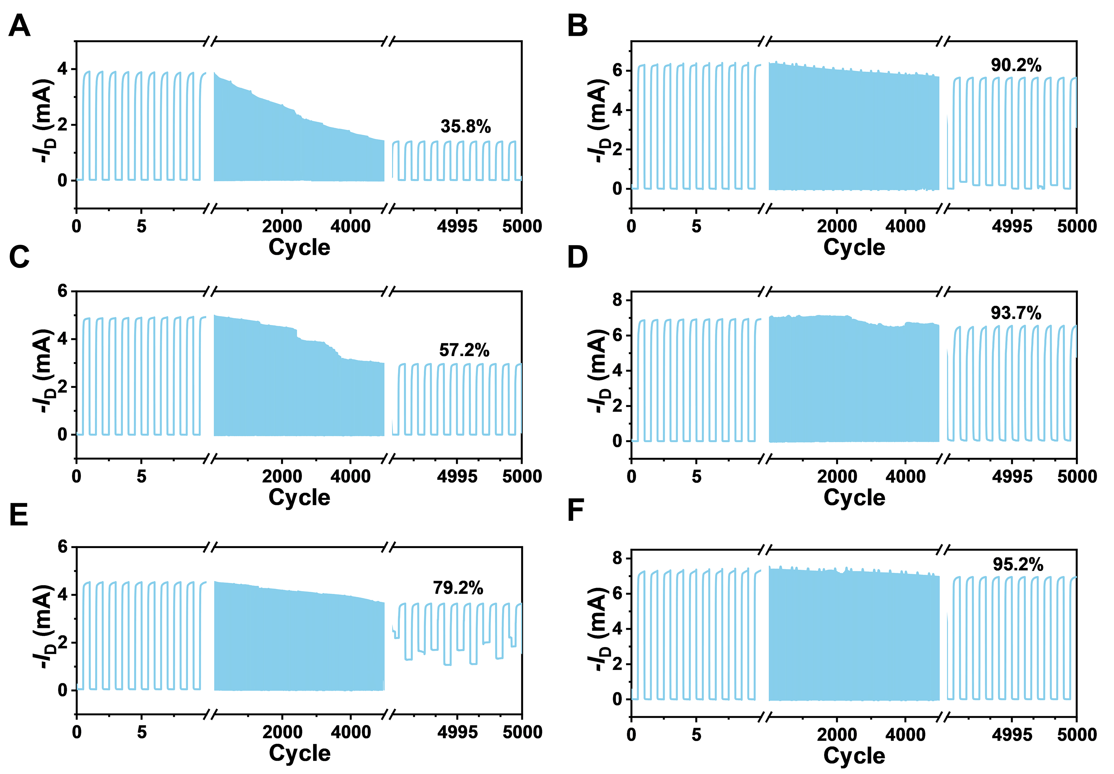
Figure 5. Stability test comprising 5,000 cycles for single-solvent devices (left) and dual-solvent devices (right ) at the same thicknesses: (A and B) 16 nm, (C and D) 25 nm, (E and F) 48 nm.
In summary, the uniform and well-ordered edge-on packing achieved through the dual-solvent strategy considerably enhances device operational stability, which provides valuable insights for developing flexible electronic devices capable of long-term, stable operation.
On the basis of the high-performance OECT devices achieved, we subsequently used them for ECG signal monitoring. As shown in Figure 6A and B, the gate electrode of the OECTs is connected to the heart, while the source electrode is connected to the left thigh (grounded). The potential difference on the body surface generated by the beating heart served as the gate voltage, and the output drain current of the OECTs was employed to monitor ECG signals in real time. A flexible device was also fabricated and placed on the wrist area to record ECG signals in real time. The recorded ECG signals [Figure 6B] exhibited a higher signal-to-noise ratio and increased stability. Overall, owing to its rapid current response and long-term operational stability, the morphologically optimized P(g2T-T) device provides a pathway for achieving high-quality and stable signals in ECG monitoring, thereby markedly expanding the potential future applications of wearable electronic devices.
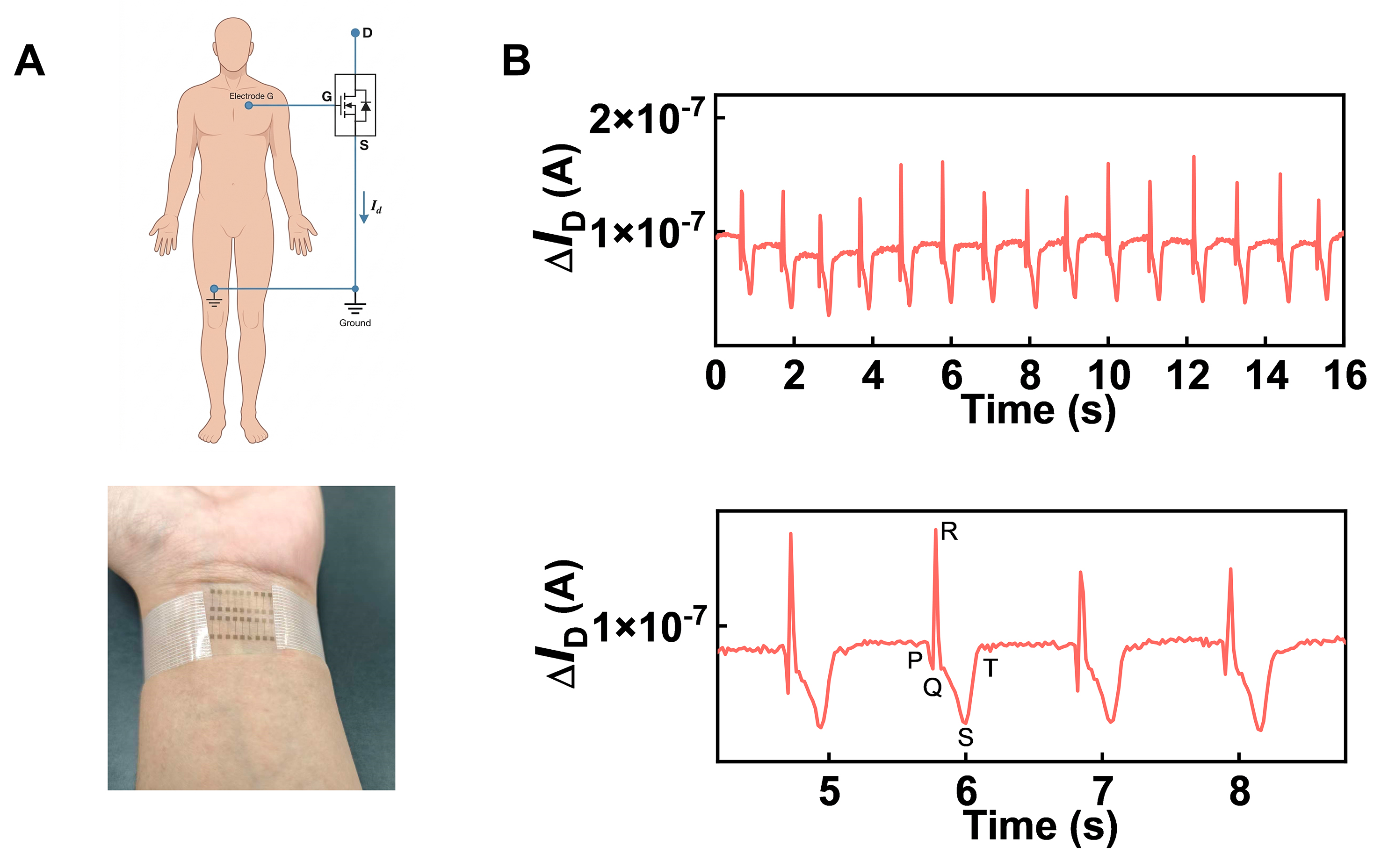
Figure 6. (A) ECG schematic illustration; (B) Corresponding ECG signal. The hand photograph is taken by the authors. ECG: Electrocardiogram.
CONCLUSIONS
In summary, in this this study, mixed ionic–electronic transport is optimized synergistically, and a satisfactory stability is achieved using a dual-solvent-mediated blade-coating strategy. Moreover, the influences of the film thickness and crystalline ordering on the performance of hydrophilic polymer films in OECTs are elucidated. The results reveal the existence of an optimal thickness window that balances ion doping efficiency with charge transport. The chloroform/acetonitrile dual-solvent system effectively modulates solution evaporation and film solidification kinetics, thereby successfully inducing the formation of a highly crystalline, edge-on oriented fibrous network structure. This structural optimization remarkably enhances both the charge carrier mobility and mechanical stability, which facilitates the simultaneous realization of efficient mixed ionic–electronic transport and excellent device stability. This study provides an effective physical pathway for the precise control of the morphology–performance relationship in organic semiconductor films, thereby offering crucial insights for the development of high-performance and stable OECTs.
DECLARATIONS
Authors’ contributions
Method, analysis, and writing of the original draft: Zhong, B.; Lu, J.
Method, analysis, and interpretation of the data: Jiang, X.; Wu, J.; Zhang, R.; Ji, S.; Liu, D.; Lu, J.
Concept, review, and revision of the manuscript: Wang, Z.; Zhang, R.; Huang, L.; Chi, L.
Availability of the data and materials
The data supporting the findings of this study are available in the article and its Supplementary Materials. All other reasonable requests can be directed to the corresponding author.
AI and AI-assisted tools statement
Not applicable.
Financial support and sponsorship
The authors acknowledge the financial support from the National Key Research and Development Program of China (2024YFB3211600), the National Natural Science Foundation of China (Grant Nos. 52573208 and 22222205), the Science and Technology Development Fund of Macao (No. 0063/2024/RIA1), the Suzhou Key Laboratory of Surface and Interface Intelligent Matter (Grant SZS2022011), and the Gusu Innovation and Entrepreneurship Talent Program - Major Innovation Team (ZXD2023002). This study was also supported by the Collaborative Innovation Center of Suzhou Nano Science and Technology. The authors thank the staff of the SSRF for the assistance provided with beamline BL14B1.
Conflicts of interest
All authors declared that there are no conflicts of interest.
Ethical approval and consent to participate
In this study, only noninvasive data collection was conducted through simple placement of devices on the skin. Research involving human subjects or data was conducted in accordance with the Declaration of Helsinki and approved by the Ethics Committee of Soochow University (SUDA20250609H08). All the participants were fully informed regarding the purpose and procedures of all the physiological electrical signal tests prior to participation, and written informed consent was obtained from all the individuals involved.
Consent for publication
Not applicable.
Copyright
© The Author(s) 2026.
Supplementary Materials
REFERENCES
1. Gerasimov, J. Y.; Tu, D.; Hitaishi, V.; et al. A biologically interfaced evolvable organic pattern classifier. Adv. Sci. 2023, 10, e2207023.
2. Gkoupidenis, P.; Koutsouras, D. A.; Malliaras, G. G. Neuromorphic device architectures with global connectivity through electrolyte gating. Nat. Commun. 2017, 8, 15448.
3. Guo, K.; Wustoni, S.; Koklu, A.; et al. Rapid single-molecule detection of COVID-19 and MERS antigens via nanobody-functionalized organic electrochemical transistors. Nat. Biomed. Eng. 2021, 5, 666-77.
4. Li, M.; Feng, W.; Lan, Y.; et al. Effects of selenium incorporation on the performance of polythiophene based organic electrochemical transistors. J. Mater. Chem. C. 2024, 12, 7935-42.
5. Liu, C.; Deng, J.; Gao, L.; et al. Multilayer porous polymer films for high‐performance stretchable organic electrochemical transistors. Adv. Electron. Mater. 2023, 9, 2300119.
6. Lu, D.; Chen, H. Solid-state organic electrochemical transistors (OECTs) based on gel electrolytes for biosensors and bioelectronics. J. Mater. Chem. A. 2024, 13, 136-57.
7. Kukhta, N. A.; Marks, A.; Luscombe, C. K. Molecular design strategies toward improvement of charge injection and ionic conduction in organic mixed ionic-electronic conductors for organic electrochemical transistors. Chem. Rev. 2022, 122, 4325-55.
8. Rivnay, J.; Inal, S.; Salleo, A.; Owens, R. M.; Berggren, M.; Malliaras, G. G. Organic electrochemical transistors. Nat. Rev. Mater. 2018, 3, 17086.
9. Doshi, S.; Forner, M. O. A.; Wang, P.; et al. Thermal processing creates water-stable PEDOT:PSS films for bioelectronics. Adv. Mater. 2025, 37, e2415827.
10. Giovannitti, A.; Sbircea, D. T.; Inal, S.; et al. Controlling the mode of operation of organic transistors through side-chain engineering. Proc. Natl. Acad. Sci. U. S. A. 2016, 113, 12017-22.
11. Huang, L.; Wang, Z.; Chen, J.; et al. Porous semiconducting polymers enable high-performance electrochemical transistors. Adv. Mater. 2021, 33, e2007041.
12. Lan, L.; Chen, J.; Hou, H.; et al. Side chain regioregularity enables high-performance and sustainable organic electrochemical transistors. CCS. Chem. 2025, 7, 1769-82.
13. Reyn, E.; Simotko, S.; Yadav, Y.; Moscovich, N.; Frey, G. L. Tunable electrochemical doping and charge transport in non-OMIEC:OMIEC blends by microstructure design. J. Mater. Chem. C. 2026, 14, 1164-76.
14. Stegerer, D.; Liu, T.; Xiong, M.; et al. Molar mass improves the performance of n-type organic electrochemical transistors. Chem. Mater. 2025, 37, 5226-33.
15. Zhu, M.; Li, P.; Li, J.; Lei, T. Molecular packing and film morphology control in organic electrochemical transistors. Mol. Syst. Des. Eng. 2022, 7, 6-20.
16. Erhardt, A.; Hochgesang, A.; Mcneill, C. R.; Thelakkat, M. A competitive n‐type OECT material via copolymerization of electron deficient building blocks. Adv. Electron. Mater. 2023, 9, 2300026.
17. Hallani, R. K.; Paulsen, B. D.; Petty, A. J. 2nd.; et al. Regiochemistry-driven organic electrochemical transistor performance enhancement in ethylene glycol-functionalized polythiophenes. J. Am. Chem. Soc. 2021, 143, 11007-18.
18. Jiang, X.; Li, B.; Xiang, C.; et al. Integrating hydrophobic and hydrophilic building blocks for high-performance organic electrochemical transistors and biosensing. Angew. Chem. Int. Ed. Engl. 2025, 64, e202505141.
19. Wang, Y.; Hamidi-Sakr, A.; Surgailis, J.; et al. The effect of the donor moiety of DPP based polymers on the performance of organic electrochemical transistors. J. Mater. Chem. C. 2021, 9, 13338-46.
20. Xiang, L.; He, Z.; Yan, C.; et al. Nanoscale doping of polymeric semiconductors with confined electrochemical ion implantation. Nat. Nanotechnol. 2024, 19, 1122-9.
21. Nielsen, C. B.; Giovannitti, A.; Sbircea, D. T.; et al. Molecular design of semiconducting polymers for high-performance organic electrochemical transistors. J. Am. Chem. Soc. 2016, 138, 10252-9.
22. Savva, A.; Hallani, R.; Cendra, C.; et al. Balancing ionic and electronic conduction for high‐performance organic electrochemical transistors. Adv. Funct. Mater. 2020, 30, 1907657.
23. Paulsen, B. D.; Tybrandt, K.; Stavrinidou, E.; Rivnay, J. Organic mixed ionic-electronic conductors. Nat. Mater. 2020, 19, 13-26.
24. Li, J.; Liu, W.; Zhang, Y.; Mei, D.; Wang, Y. Development of highly sensitive iontronic‐based tri‐modal tactile sensor for proximity‐pressure‐temperature sensing. Adv. Mater. Technol. 2025, e00861.
25. Zhu, G.; Chen, J.; Duan, J.; et al. Fluorinated alcohol-processed n-type organic electrochemical transistor with high performance and enhanced stability. ACS. Appl. Mater. Interfaces. 2022, 14, 43586-96.
26. Huang, W.; Chen, J.; Yao, Y.; et al. Vertical organic electrochemical transistors for complementary circuits. Nature 2023, 613, 496-502.
27. Li, C. Y.; Jiang, G. H.; Higashihara, T.; Lin, Y. C. Interfacial stabilization of organic electrochemical transistors conferred using polythiophene-based conjugated block copolymers with a hydrophobic coil design. ACS. Appl. Mater. Interfaces. 2024, 16, 52753-65.
28. Liu, G.; Wen, W.; Shan, C.; et al. Photomediated ion dynamics enables multi-modal learning, memory and sensing in ultralow-voltage organic electrochemical device. Nat. Commun. 2025, 16, 6933.
29. Qin, S.; Sun, Z.; Li, H.; Rahman, C.; Gartner, T. E. 3rd.; Reichmanis, E. Organic mixed ionic-electronic conductors for organic electrochemical transistors: sidechain structure influences ion uptake and functional performance. Chemphyschem 2025, 26, e202500403.
30. Hu, Z.; Gu, P.; Yang, X.; et al. Nanoporous conjugated polymer aerogel films for high‐performance electrochemical transistors. Adv. Funct. Mater. 2024, 34, 2410788.
31. Ohayon, D.; Druet, V.; Inal, S. A guide for the characterization of organic electrochemical transistors and channel materials. Chem. Soc. Rev. 2023, 52, 1001-23.
32. Tung, Y.; Li, C.; Huang, Y.; Lin, Y. Strategically tailoring porous polythiophene nanofibers in organic electrochemical transistors to facilitate the anion doping. ACS. Electrochem. 2025, 1, 1164-75.
33. He, Z.; Chen, J.; Keum, J. K.; Szulczewski, G.; Li, D. Improving performance of TIPS pentacene-based organic thin film transistors with small-molecule additives. Org. Electron. 2014, 15, 150-5.
34. Paterson, A. F.; Savva, A.; Wustoni, S.; et al. Water stable molecular n-doping produces organic electrochemical transistors with high transconductance and record stability. Nat. Commun. 2020, 11, 3004.
35. Hidalgo Castillo, T. C.; Moser, M.; Cendra, C.; et al. Simultaneous performance and stability improvement of a p-type organic electrochemical transistor through additives. Chem. Mater. 2022, 34, 6723-33.
36. Savva, A.; Ohayon, D.; Surgailis, J.; et al. Solvent engineering for high‐performance n‐type organic electrochemical transistors. Adv. Electron. Mater. 2019, 5, 1900249.
37. Zhang, L.; Kuang, Y.; Ye, G.; Liu, J. Tailoring the density of state of n-type conjugated polymers through solvent engineering for organic electrochemical transistors. ACS. Appl. Mater. Interfaces. 2024, 16, 39693-700.
38. Flagg, L. Q.; Bischak, C. G.; Onorato, J. W.; Rashid, R. B.; Luscombe, C. K.; Ginger, D. S. Polymer crystallinity controls water uptake in glycol side-chain polymer organic electrochemical transistors. J. Am. Chem. Soc. 2019, 141, 4345-54.
39. Flagg, L. Q.; Cho, W.; Woodcock, J.; et al. Improved organic electrochemical transistors via directed crystallizable small molecule templating. Chem. Mater. 2024, 36, 1352-61.
40. Song, J. H.; Kim, Y.; Yoo, H.; Lee, E. K. Kinetic swelling-driven PTG interlayers for enhanced crystallinity and charge transport in polymer OECTs. J. Mater. Chem. C. 2025, 13, 17801-12.
41. Kang, S.; Fan, J.; Gupta, M. Optimization of drop-casting parameters for fabrication of n-type accumulation mode organic electrochemical transistors (OECTs) using gNDI-Br2. Mater. Adv. 2026, 7, 960-8.
42. Zhang, C.; Meng, J.; Chen, Y.; et al. Carbon nanotube/polymer hybrid film for optimizing electron transport in organic electrochemical transistor. J. Mater. Sci. 2023, 58, 15727-37.
43. Giovannitti, A.; Nielsen, C. B.; Sbircea, D. T.; et al. N-type organic electrochemical transistors with stability in water. Nat. Commun. 2016, 7, 13066.
44. Flagg, L. Q.; Giridharagopal, R.; Guo, J.; Ginger, D. S. Anion-dependent doping and charge transport in organic electrochemical transistors. Chem. Mater. 2018, 30, 5380-9.
45. Jiang, X.; Wang, Q.; Wang, Z.; Dong, B.; Huang, L.; Chi, L. Recent progresses on the high performance organic electrochemical transistors. Chem. Res. Chin. Univ. 2021, 37, 975-88.
46. Bardagot, O.; Durand, P.; Guchait, S.; et al. Over tenfold increase in current amplification due to anisotropic polymer chain alignment in organic electrochemical transistors. Adv. Mater. 2025, 37, e2420323.
47. Diao, Y.; Tee, B. C.; Giri, G.; et al. Solution coating of large-area organic semiconductor thin films with aligned single-crystalline domains. Nat. Mater. 2013, 12, 665-71.
48. Lu, Z.; Wang, C.; Deng, W.; Achille, M. T.; Jie, J.; Zhang, X. Meniscus-guided coating of organic crystalline thin films for high-performance organic field-effect transistors. J. Mater. Chem. C. 2020, 8, 9133-46.
49. Pierre, A.; Sadeghi, M.; Payne, M. M.; Facchetti, A.; Anthony, J. E.; Arias, A. C. All-printed flexible organic transistors enabled by surface tension-guided blade coating. Adv. Mater. 2014, 26, 5722-7.
50. Sirringhaus, H. 25th anniversary article: organic field-effect transistors: the path beyond amorphous silicon. Adv. Mater. 2014, 26, 1319-35.
51. Yildiz, O.; Wang, Z.; Brzezinski, M.; et al. Role of meniscus shape on crystallization of molecular semiconductors and fluid dynamics during meniscus‐guided coating. Adv. Funct. Mater. 2024, 34, 2314131.
52. Li, Y.; Liu, H.; Wu, J.; et al. Additive and high-temperature processing boost the photovoltaic performance of nonfullerene organic solar cells fabricated with blade coating and nonhalogenated solvents. ACS. Appl. Mater. Interfaces. 2021, 13, 10239-48.
53. Jeong, D.; Jo, I.; Lee, S.; et al. High‐performance n‐type organic electrochemical transistors enabled by aqueous solution processing of amphiphilicity‐driven polymer assembly. Adv. Funct. Mater. 2022, 32, 2111950.
54. Deegan, R. D.; Bakajin, O.; Dupont, T. F.; Huber, G.; Nagel, S. R.; Witten, T. A. Capillary flow as the cause of ring stains from dried liquid drops. Nature 1997, 389, 827-9.
55. Jiang, Z.; Tao, L.; Yang, X.; Doi, M.; Xu, Y.; Man, X. Uniform deposition of particles in large scale by drying of binary droplets. Small 2025, 21, e2501549.
56. Yang, M.; Chen, D.; Hu, J.; Zheng, X.; Lin, Z.; Zhu, H. The application of coffee-ring effect in analytical chemistry. TrAC. Trends. Anal. Chem. 2022, 157, 116752.
57. Shi, G.; Huang, Z.; Qiao, R.; et al. Manipulating solvent fluidic dynamics for large-area perovskite film-formation and white light-emitting diodes. Nat. Commun. 2024, 15, 1066.
58. Du, Z.; Zhou, H.; Yu, X.; Han, Y. Controlling the polarity and viscosity of small molecule ink to suppress the contact line receding and coffee ring effect during inkjet printing. Colloids. Surf. A. Physicochem. Eng. Asp. 2020, 602, 125111.
59. Lim, J.; Lee, W.; Lee, H.; Lee, J.; Park, Y.; Cho, K. Self‐organization of ink‐jet‐printed triisopropylsilylethynyl pentacene via evaporation‐induced flows in a drying droplet. Adv. Funct. Mater. 2008, 18, 229-34.
60. He, Z.; Asare-Yeboah, K.; Bi, S. Grain boundary engineering for high-mobility organic semiconductors. Electronics 2025, 14, 3042.
61. Kim, S. M.; Kim, C. H.; Kim, Y.; et al. Influence of PEDOT:PSS crystallinity and composition on electrochemical transistor performance and long-term stability. Nat. Commun. 2018, 9, 3858.
62. Giridharagopal, R.; Flagg, L. Q.; Harrison, J. S.; et al. Electrochemical strain microscopy probes morphology-induced variations in ion uptake and performance in organic electrochemical transistors. Nat. Mater. 2017, 16, 737-42.
63. Keene, S. T.; Rao, A.; Malliaras, G. G. The relationship between ionic-electronic coupling and transport in organic mixed conductors. Sci. Adv. 2023, 9, eadi3536.
64. Wu, X.; Surendran, A.; Ko, J.; et al. Ionic-liquid doping enables high transconductance, fast response time, and high ion sensitivity in organic electrochemical transistors. Adv. Mater. 2019, 31, e1805544.
65. Guo, J.; Chen, S. E.; Giridharagopal, R.; et al. Understanding asymmetric switching times in accumulation mode organic electrochemical transistors. Nat. Mater. 2024, 23, 656-63.
66. Paudel, P. R.; Skowrons, M.; Dahal, D.; Radha Krishnan, R. K.; Lüssem, B. The transient response of organic electrochemical transistors. Adv. Theory. Simul. 2022, 5, 2100563.
67. Shiri, P.; Dacanay, E. J. S.; Hagen, B.; Kaake, L. G. Vogel–Tammann–Fulcher model for charging dynamics in an organic electrochemical transistor. J. Mater. Chem. C. 2019, 7, 12935-41.
68. Zhao, C.; Yang, J.; Ma, W. Transient response and ionic dynamics in organic electrochemical transistors. Nanomicro. Lett. 2024, 16, 233.
69. Maria, I. P.; Griggs, S.; Rashid, R. B.; et al. Enhancing the backbone coplanarity of n-type copolymers for higher electron mobility and stability in organic electrochemical transistors. Chem. Mater. 2022, 34, 8593-602.
70. Su, S.; Shimizu, H.; Matsuda, M.; et al. Mobility and stability enhancements of conjugated polymers with diastereomeric conjugation break spacers in organic electrochemical transistors. Macromolecules 2025, 58, 5807-20.
Cite This Article
 Open Access
How to Cite
Download Citation
Export Citation File:
Type of Import
Tips on Downloading Citation
Citation Manager File Format
Type of Import
Direct Import: When the Direct Import option is selected (the default state), a dialogue box will give you the option to Save or Open the downloaded citation data. Choosing Open will either launch your citation manager or give you a choice of applications with which to use the metadata. The Save option saves the file locally for later use.
Indirect Import: When the Indirect Import option is selected, the metadata is displayed and may be copied and pasted as needed.
About This Article
Special Topic
Copyright

Data & Comments
Data
0











Comments
Comments must be written in English. Spam, offensive content, impersonation, and private information will not be permitted. If any comment is reported and identified as inappropriate content by OAE staff, the comment will be removed without notice. If you have any queries or need any help, please contact us at [email protected].