

fig3
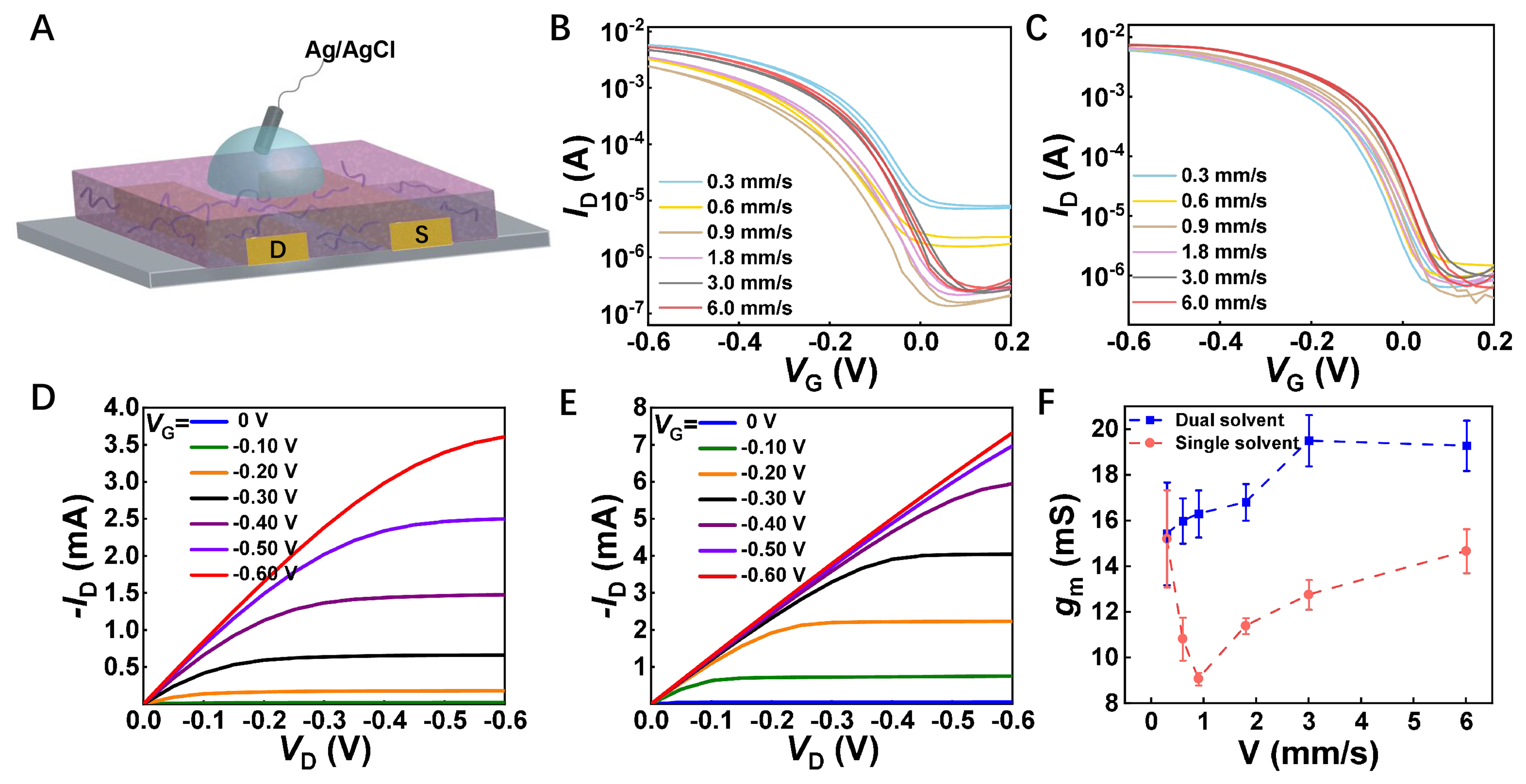
Figure 3. (A) Schematic illustration of the device structure; (B) Transfer curves for films formed with the single-solvent system at different coating speeds; (C) Transfer curves for films formed with the dual-solvent system at different coating speeds; (D) Output curve of the film formed with the single-solvent system at a velocity of 1.8 mm/s; (E) Output curve of the film formed with the dual-solvent system at a velocity of 1.8 mm/s; (F) Comparison of peak transconductance between the single- and dual-solvent devices at different blade-coating speeds. The error bars indicate the standard deviation (each point represents n ≥ 10 independent devices). The channel width (W) is