


Principles and applications of ultrafast transmission electron microscopy
 0
0 
Abstract
Ultrafast transmission electron microscopy (UTEM) is an advanced experimental technique that integrates a femtosecond (fs) laser with transmission electron microscopy to capture material dynamic processes at exceptionally high spatiotemporal resolution. This review aims to provide an overview on the recent progresses on UTEM from technical principles, instrument developments to scientific applications and future prospects. The fundamental operation principle of UTEM involves exciting the sample with a pump laser/electric pulse, followed by probing with a time-delayed electron pulse. By precisely varying the delay time between the pump and probe pulses, electron imaging, diffraction or spectroscopy at fs-nanometer/atomic scale can be achieved. Based on these capabilities, these advances have recently culminated in techniques such as five-dimensional scanning transmission electron microscopy and Attosecond electron microscopy, which push the boundaries toward quantitative strain mapping and sub-cycle dynamics. UTEM has demonstrated significant applications in the study of microscopic dynamics in correlated materials, semiconductors, catalysts, nanophotonics, etc. It enables direct visualization of fundamental dynamic processes such as carrier relaxation, lattice vibrations, phase transitions, near-field evolution and magnetic domain switching, etc., thereby deepening the understanding of non-equilibrium states and providing critical insights for the design of novel functional devices. With ongoing advancements in fs electron sources and high-sensitivity electron detectors, the temporal resolution and detection sensitivity of UTEM continue to improve, highlighting its substantial potential in nanometer/atomic-scale ultrafast science. Future technique developments are expected to drive major breakthroughs in condensed matter physics, materials science, chemical reactions and even biological structure dynamics, offering a powerful tool for exploring the ultrafast microscopic world.
Keywords
INTRODUCTION
Ultrafast transmission electron microscopy (UTEM) represents a transformative advancement in dynamic characterization of materials, synergistically integrating the high spatial resolution (from nanoscale down to atomic scale) of conventional transmission electron microscopy (TEM) with ultrafast temporal resolution (from nanoseconds down to femtoseconds) of ultrafast laser. This capability enables the direct spatiotemporal probing of photoinduced nonequilibrium processes, including structural phase transitions[1,2], carrier dynamics[3], exciton dynamics[4], and electromagnetic responses[5]. Operating on a “photon-pump, electron-probe” principle[6], UTEM employs femtosecond (fs) laser pulses to generate ultrashort electron packets from a photocathode inside the TEM. These electron pulses serve as a probe beam that surpasses the optical diffraction limit, permitting the visualization of ultrafast dynamics with combined high spatial and temporal precision[7,8].
In recent years, researchers worldwide have made significant progresses in the developments and applications of UTEM technology since it was pioneered by Ahmed H. Zewail group in 2005, which is also termed as four-dimensional electron microscopy (4D-EM)[9]. Several electron pulse compression and modulation techniques have been developed in UTEM, pushing the temporal resolution to the fs and even attosecond as scale[10]. Various environmentally controllable UTEM systems have also been developed, enabling dynamic research in multi-field conditions[11]. Over the past decades, UTEM has undergone a transformative evolution from proof-of-principle demonstrations to integrated system development, emerging as a cornerstone experimental platform for probing non-equilibrium dynamics of material structures and electronic states at extreme spatiotemporal scales (picosecond-to-femtosecond temporal and nanometer-to-atomic spatial resolution). Its technical scope has expanded from mere “ultrafast imaging” to a comprehensive characterization framework that integrates time-resolved diffraction, spectroscopy, in situ stimuli, and artificial intelligence-assisted analysis[12]. Notably, the emergence of five-dimensional scanning transmission electron microscopy (5D-STEM) has enabled quantitative mapping of transient strain fields and phonon dispersion with nanometer-femtosecond precision, representing a paradigm shift in multidimensional dynamic characterization. Despite these achievements, the UTEM technique still faces persistent challenges. For instance, the simultaneous optimization of temporal and spatial resolution remains difficult, quantitative frameworks for complex nonequilibrium processes are underdeveloped, and atomic-scale ultrafast imaging capabilities require further refinement. These limitations currently constrain deeper applications in emerging quantum and energy-conversion materials. However, the field is advancing rapidly and is highly interdisciplinary. Diverse technical pathways (e.g., photocathode-driven emission[13], all-radio-frequency compression[14,15], attosecond pulse generation[16]) and fragmented application landscapes (spanning quantum materials[17], energy chemistry[18], bio-imaging[19], etc.) have emerged. A systematic effort to elucidate the intrinsic logic of its technological evolution, the scientific connections between its multimodal detection capabilities, and the strategy for selecting and optimizing technical pathways for specific scientific questions is still lacking.
To address this gap, this review systematically examines the evolution, operational principles, and application landscapes of UTEM technique, aiming to bridge the complete chain from fundamental principles and instrumentation to scientific applications. By synthesizing the strengths and applicable scopes of different technical schemes and analyzing representative cutting-edge studies, we elucidate how UTEM unveils transient microscopic mechanisms inaccessible to conventional techniques. Our goal is to provide the community with a reference that combines technical insight and scientific foresight, thereby fostering the application of UTEM to address critical challenges in condensed matter physics, materials science, and chemical dynamics at greater depth and breadth.
This review is organized to guide the reader from the foundational principles of UTEM to its most advanced applications and future directions. We begin in Section "OVERVIEW OF UTEM TECHNOLOGY" with an overview of the historical development and technical framework of UTEM, establishing the context for its emergence. Section "PRINCIPLES AND TECHNIQUES OF UTEM" details the working principles, including both laser-based and laser-free approaches, with emphasis on the electron source dynamics and the trade-offs between temporal resolution, spatial resolution, and electron flux. Section "SCIENTIFIC APPLICATIONS OF UTEM" constitutes the core of the review, presenting the scientific applications of UTEM organized by the type of dynamic information extracted: ultrafast structural dynamics (imaging and diffraction), magnetic dynamics (Lorentz TEM), multidimensional strain mapping (5D-STEM), electronic dynamics (Time-Resolved Electron Energy Loss Spectroscopy, EELS), and light-matter interactions (Photon-Induced Near-field Electron Microscopy, PINEM). This classification reflects the distinct experimental modalities and the complementary insights they provide. Section "ATTOSECOND ELECTRON MICROSCOPY AND APPLICATIONS" addresses the frontier of attosecond electron microscopy, discussing its principles, technical milestones, and emerging applications. Finally, Section "OUTLOOK" concludes with a summary of key achievements, an analysis of remaining challenges, and a forward-looking perspective on the technological advancements expected to shape the future of UTEM.
OVERVIEW OF UTEM TECHNOLOGY
UTEM combines fs laser pump-probe technology with conventional TEM to achieve high spatiotemporal analysis of dynamic processes in matter, with spatial resolution reaching the sub-nanometer (nm) level and temporal resolution entering the fs or even attosecond regime. This section provides an overview of its historical evolution and technical framework. Since the invention in the 1930s, TEM has become a core tool for revealing the static microstructure of matter at atomic scale, enabling precise characterization of material morphology, crystal structure, and chemical composition. In recent years, in situ dynamic TEM techniques have rapidly developed. By introducing various external field stimuli such as acoustic, optical, thermal, electrical, and magnetic fields[20-22], it has become possible to study physical and chemical dynamic processes on time scales from milliseconds to microseconds However, limited by conventional detection mechanisms, standard TEM struggles to capture ultrafast processes on picosecond (ps) to fs scales, such as key transient phenomena including carrier dynamics, chemical bond breaking, lattice vibrations, phase transitions, and exciton migration. The invention of the ruby laser in the 1960s provided a key opportunity to break this temporal resolution bottleneck, and the subsequently developed pump-probe technique laid the methodological foundation for enhancing the temporal resolution of electron microscopy. By the 1980s, Professor Bostanjoglo's team at the Technical University of Berlin first proposed the concept of pulsed electron imaging[23]. Entering the 21st century, Nobel Laureate Ahmed H. Zewail and his team successfully integrated fs laser pulses with electron microscopy, pioneering 4D-EM[9]. This achievement marked the formal birth of UTEM, pushing the temporal resolution of TEM to the fs and even attosecond scale. After nearly two decades of continuous development, UTEM has become a revolutionary dynamic observation tool in interdisciplinary fields such as condensed matter physics, materials science, photochemistry, and structural biology[24-28].
PRINCIPLES AND TECHNIQUES OF UTEM
Working principle of UTEM
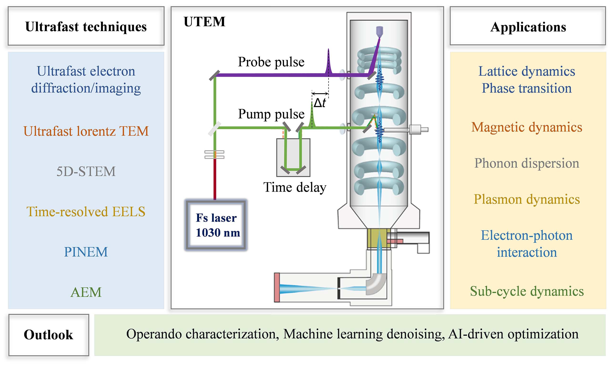
UTEM achieves its ultrafast temporal resolution through the core principle of pump-probe technology. A fs pump laser pulse excites the sample, initiating the target dynamic process (such as carrier excitation or lattice deformation)[29]. Unlike optical pump-probe techniques, UTEM employs a delayed, controllable ultrashort electron pulse (generated by ultraviolet fs laser pulse excitation on the photocathode inside the modified TEM) as the probe to perform imaging or diffraction analysis on the sample in its excited state. By precisely scanning the time interval (Δt) between the pump laser and probe electron pulses, the complete temporal evolution of the dynamic process can be captured [Figure 1].
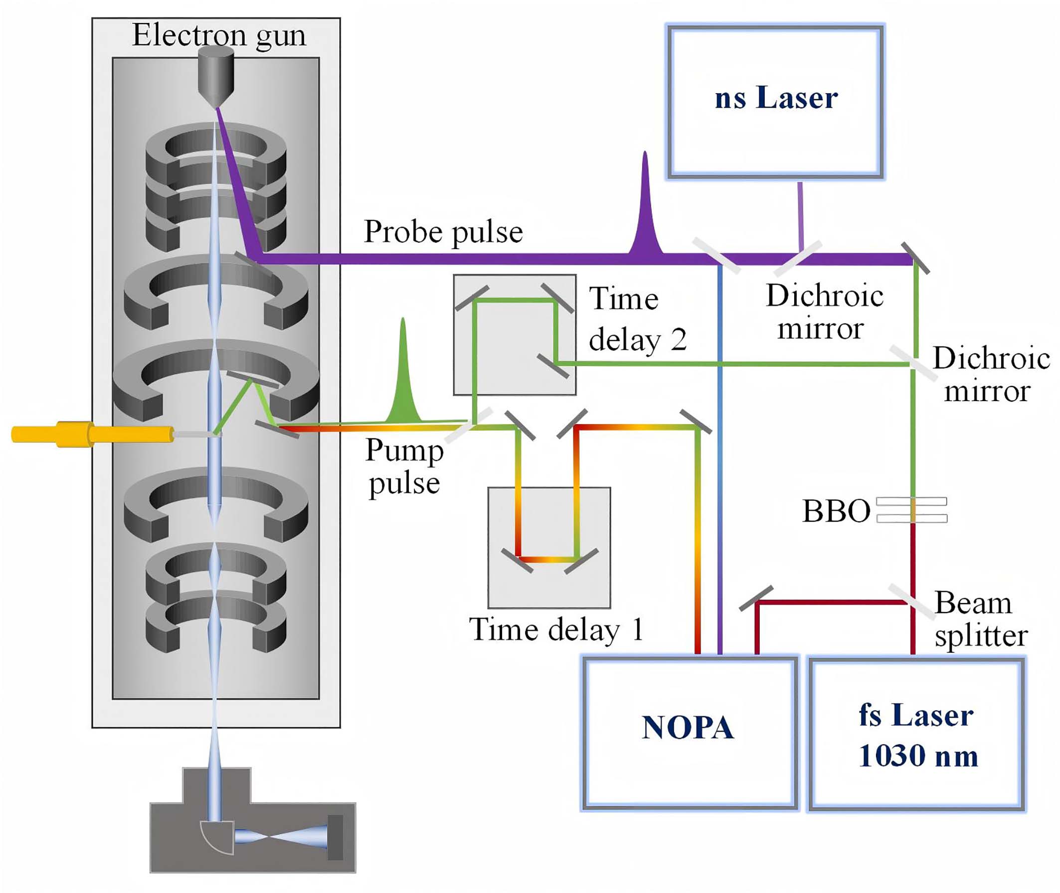
Figure 1. Schematic diagram of an UTEM setup.
In terms of photocathode materials and electron emission, commonly used photocathode materials include gold (Au) and gallium nitride (GaN), while TEM filaments typically use tungsten or lanthanum hexaboride (LaB6). Regarding pulse generation mechanisms, ultraviolet are directed onto the cathode surface, emitting photoelectrons via single-photon or multi-photon absorption. The generated electron pulse width is influenced by both the laser pulse width and the cathode materials band structure. Reviewing the development history, in the early 2000s, researchers introduced nanosecond (ns) lasers into the electron gun, achieving imaging and diffraction based on single ns electron pulses[30], which were successfully applied to study irreversible kinetic processes[31]. However, in this single-shot imaging/diffraction mode, as each pulse needs to contain a large number of electrons, severe space-charge effects limit the temporal resolution to the ns scale. In 2005, Professor Ahmed Zewail's team at Caltech achieved a key breakthrough. They used a fs laser to generate electron pulses containing only a few or even single electrons per pulse, effectively avoiding space-charge effects and achieving UTEM temporal resolution at the sub-picosecond level[9]. This fs laser-based UTEM is particularly suitable for studying reversible kinetic processes where the sample fully recovers to the ground state between consecutive pump pulses. Recently, it has been widely applied to high-spatiotemporal-resolution studies of photoinduced ultrafast dynamics in matters.
Instrumentation of UTEM systems
A typical schematical diagram of an UTEM system are shown in Figure 1, consisting mainly of an ultrafast laser system and a TEM. The ultrafast laser system includes components such as a laser source, a delay stage, frequency doubling crystals, and an optical parametric amplifier (OPA). The output near-infrared fs laser is typically split into two beams: one is frequency-tripled or quadrupled and directed into the TEM electron gun to excite the photocathode for generating pulsed electron beams; the other fs laser beam is wavelength-tuned via a frequency doubling crystal or an OPA and then is directed into the sample chamber to excite the sample for inducing dynamic processes. With their extremely short pulse width and high peak power density, fs lasers enable ultrafast excitation of materials, inducing rich photoinduced dynamic changes. Additionally, ns lasers can also be introduced into the electron gun to generate ns-scale electron pulses to meet the needs of ns time-resolved kinetic studies. High-precision optical delay stages are used to precisely adjust the optical path difference between the pump and probe pulses, thereby achieving time-resolved electron imaging, diffraction or spectroscopy. The OPA is used to generate wavelength-tunable fs laser pulses, enabling flexible control of sample excitation conditions. For the electron microscope part, commercial TEMs are typically modified by installing mirrors inside the column and opening optical windows on the column wall to enable guiding the pump and probe laser pulses to the sample and the electron gun cathode, respectively. The pump laser is focused by a lens onto the sample surface, while the probe laser is incident on the photocathode surface in the electron gun to generate pulsed electron beams.
Besides the typical laser-based UTEM, there is another type of stroboscopic UTEM technique without laser sources, which can be dated back to the 1960s-70s[32,33]. Recently, this probing approach has regained academic attention[34]. The main advantage of this technology is that it does not require modification of the electron source. Instead, electrostatic or radio-frequency (RF) beam deflection devices are introduced into the TEM column to rapidly sweep the continuous electron beam across a fixed small aperture, thereby slicing the continuous beam into short pulses [Figure 2A][14,35-37]. This method effectively preserves the original electron source's coherence and energy spread, and the switching between pulsed and continuous emission modes is particularly convenient. Currently, this technique has achieved a temporal resolution of hundreds of femtoseconds[14]. Its inherent gigahertz repetition rate, combined with a high duty cycle (about 10%-20%, i.e., the effective electron utilization ratio)[38], allows for significantly reduced data acquisition time while ensuring signal-to-noise ratio. However, the high repetition rate also limits the range of materials that can be studied with the pump-probe techniques, as it requires the excited-state lifetime of the material under study to be on the ns scale. To date, laser-free stroboscopic TEM has been successfully applied to image electromagnetic wave propagation in micro/nanostructures [Figure 2B][14] and to probe magnetization dynamics in magnetic vortices [Figure 2C and D][15] under RF excitation. Other excitation methods specifically designed for chemical kinetics studies (such as visible light irradiation or thermal excitation) are expected to emerge in the coming years. These new technologies offer broad application prospects for revealing magnetic, plasmonic, and excitonic dynamics in functional materials[38].
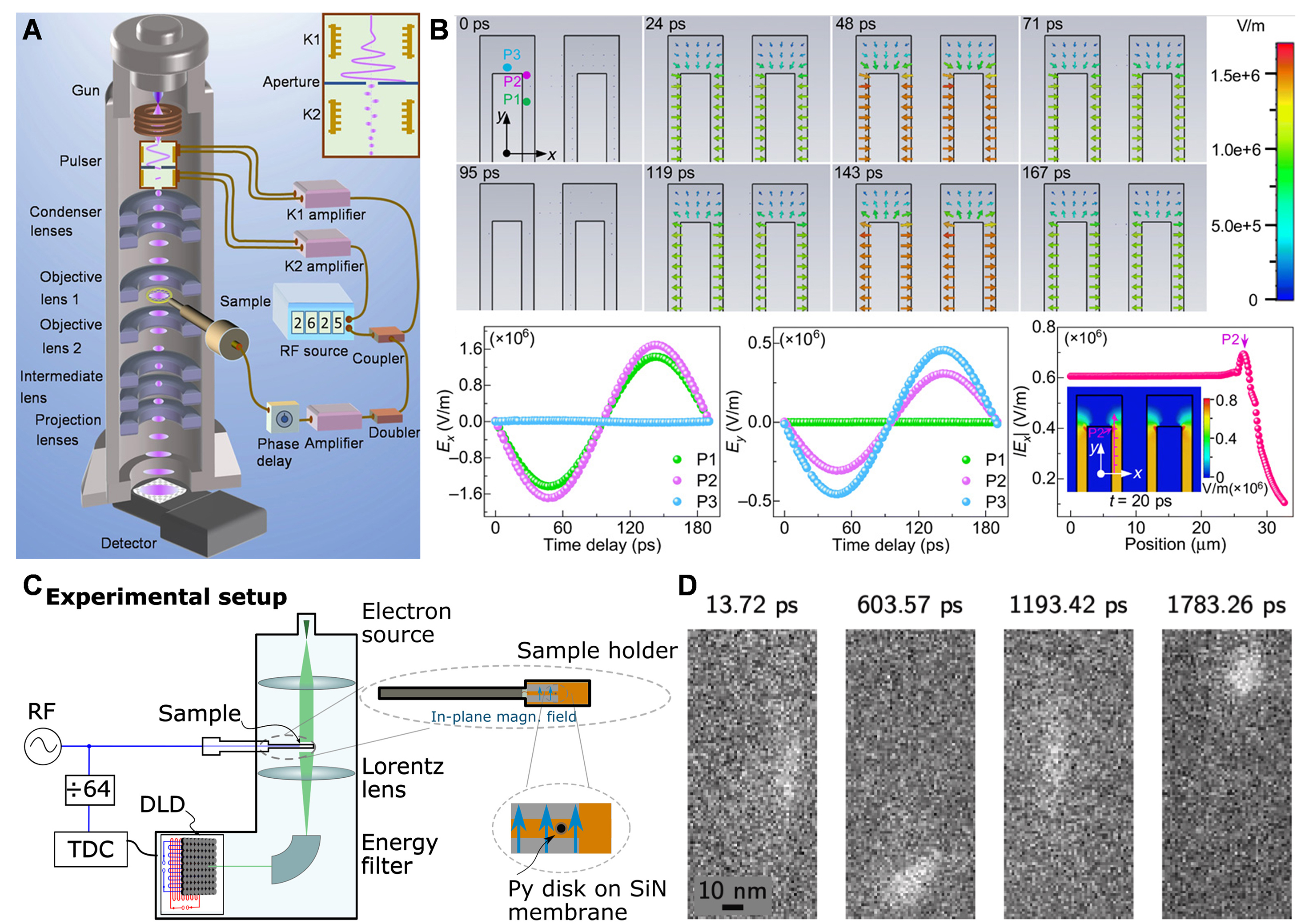
Figure 2. Laser-free UTEM. (A) Laser-free UTEM by integrating ultrafast RF pulser into a TEM. Main column elements of the RF pulser: kickers (K1, K2) and aperture as shown in the inset. Reprinted with permission[14]. Copyright 2020, AAAS. (B) Reconstructed electromagnetic wave propagation dynamics in two interdigitated combs. Reprinted with permission[14]. Copyright 2020, AAAS. (C) Laser-free UTEM based on a delay line detector. Reprinted with permission[15]. (C) is reproduced under the CC BY-NC-ND license. Copyright 2022, Elsevier. (D) Snapshots of magnetic vortex core motion recorded at different time steps over a 13 ps interval during excitation at 417 MHz under an 18 mT static out-of-plane applied magnetic field. The images reveal clockwise motion of the magnetic vortex core. Reprinted with permission[15]. Copyright 2022, Elsevier.
Working kinetics and temporal resolution
UTEM enables direct visualization of structural dynamics over a wide temporal window through a pump-probe scheme, in which an ultrafast laser pulse excites the specimen and a time-delayed electron pulse probes the transient structural response[39]. By systematically scanning the delay time between the pump and probe pulses, the time evolution of microscopic processes can be reconstructed with high temporal precision, allowing UTEM to capture nonequilibrium structural dynamics spanning multiple characteristic timescales from femtoseconds to nanoseconds.
The working kinetics accessible by UTEM typically cover several key stages of ultrafast processes in condensed matter systems. Immediately after photoexcitation, nonequilibrium electronic distributions are formed within tens to hundreds of femtoseconds, followed by electron-phonon coupling processes occurring on sub-picosecond timescales[25]. Subsequently, lattice heating, structural relaxation, and phase transition dynamics generally develop on picosecond to nanosecond timescales, while domain evolution and defect migration may extend to even longer temporal regimes. Benefiting from its capability of combining nanometer spatial resolution with ultrafast temporal resolution, UTEM provides a unique platform for correlating these multiscale structural dynamics across both reciprocal space and real space[29].
The temporal resolution of UTEM is primarily determined by two factors: the duration of the probe electron pulse and the synchronization jitter between the pump and probe pulses. In laser-driven photocathode-based UTEM systems, the initial electron pulse width is closely related to the laser pulse duration and the emission dynamics of the photocathode material[40]. The kinetic process of photoelectron emission is governed by the laser fluence, pulse duration, and the band structure of the cathode material. Under low-fluence excitation, single-electron or few-electron pulses are generated, minimizing space-charge effects and enabling sub-picosecond temporal resolution. With optimized emission conditions, femtosecond electron pulses can be routinely generated in modern UTEM platforms. However, coulomb repulsion between electrons within a pulse (space-charge effect) leads to temporal broadening and spatial expansion during propagation from the photocathode to the specimen plane. This effect becomes particularly severe when higher bunch charges are required for single-shot experiments or for detecting weak signals. To suppress space-charge induced broadening, UTEM experiments are often operated in the single-electron regime or under low-charge conditions. Additionally, RF cavity compression and terahertz-based pulse manipulation techniques have been demonstrated as effective approaches for shortening electron pulse duration and improving temporal resolution[14,15]. Timing jitter originating from laser fluctuations, electronic triggering systems, and mechanical delay stages may introduce additional temporal uncertainty in pump-probe measurements[41]. To overcome this limitation, synchronization schemes have been developed. For instance, phase-locked loops that synchronize microwave compression cavities directly with the mode-locked femtosecond oscillator have achieved timing stabilities below 5 fs RMS[42]. Alternatively, passive optical synchronization using master-slave laser configurations has demonstrated timing jitter as low as 0.74 fs[43]. More recently, hybrid methodologies combining weak value amplification with deep learning have been proposed to suppress residual timing jitter, enabling attosecond-scale precision in pump-probe measurements[44]. These advances have significantly improved the temporal precision of ultrafast electron microscopy experiments.
In addition to the intrinsic timescales of the physical processes, the accessible working kinetics in UTEM experiments are also influenced by the repetition rate of the pump-probe scheme and the reversibility of the investigated processes. For reversible structural dynamics, stroboscopic acquisition allows signal accumulation over millions of excitation cycles, enabling high signal-to-noise imaging of weak transient structural changes[45]. In contrast, irreversible processes require single-shot or low-repetition-rate acquisition modes, in which the temporal resolution is determined by the duration of a single electron pulse[31]. The combination of these acquisition strategies enables UTEM to investigate a broad range of ultrafast phenomena under both reversible and irreversible conditions[46].
With recent advances in photocathode design, RF compression cavities, and optical gating techniques, the temporal resolution of UTEM has been further improved toward the few-tens-of-femtoseconds regime, and even attosecond electron pulse generation has been proposed in next-generation ultrafast electron microscopy platforms[29,47]. These developments continue to expand the accessible working kinetics of UTEM and open new opportunities for probing elementary structural dynamics at their fundamental time scales. Therefore, UTEM provides a powerful approach for mapping multiscale structural kinetics ranging from ultrafast electronic excitation to lattice phase transitions and mesoscale structural evolution, enabling comprehensive understanding of dynamic processes in quantum materials, low-dimensional systems, and functional nanostructures.
Spatial resolution
While conventional TEM routinely achieves atomic resolution under static conditions, attaining comparable spatial resolution in UTEM is considerably more challenging due to several interconnected factors that often involve trade-offs with temporal resolution and electron flux.
Under low-fluence operation where single-electron or few-electron pulses are used to minimize space-charge effects, the achievable spatial resolution is primarily limited by the intrinsic brightness of the photocathode source and the aberrations of the electron optics, typically reaching sub-nanometer to nanometer levels[48]. However, when higher bunch charges are required. For instance, to achieve sufficient signal in single-shot experiments or to detect weak transient signals, space-charge-induced Coulomb repulsion not only broadens the pulse duration (degrading temporal resolution) but also degrades transverse coherence and increases the effective source size, leading directly to a loss of spatial resolution. This inherent trade-off between electron flux, temporal resolution, and spatial resolution represents a fundamental constraint in UTEM design and operation. The spatial resolution in UTEM is also strongly influenced by the specific technical approach. Photoinjector-based systems that generate electron pulses directly from a laser-illuminated photocathode can achieve high brightness but are susceptible to energy spread and emittance growth, which can limit spatial coherence. Alternatively, beam-blanking approaches that slice a continuous electron beam preserve the original source coherence and energy spread, thereby maintaining spatial resolution comparable to conventional TEM, but at the cost of lower temporal resolution and duty cycle[14,15]. The choice of photocathode material also plays a critical role: Schottky emitters offer high brightness and stability but require careful synchronization with ultrafast lasers, while field-emitter tips and nanotip sources can provide extreme brightness and coherence but present significant challenges in pulse generation and long-term stability[13]. Beyond instrumental factors, the sample itself can affect the effective spatial resolution. Under ultrafast excitation, pump-induced structural changes such as lattice expansion, phase separation, or surface charging can introduce transient distortions that blur high-resolution features. Additionally, the high peak power of femtosecond laser pulses can induce sample damage or heating, necessitating careful trade-offs between excitation strength and spatial fidelity. For beam-sensitive materials, the cumulative electron dose over multiple pump-probe cycles may also lead to radiation damage that degrades spatial resolution over the course of an experiment.
Looking forward, several strategies are expected to push the spatial resolution of UTEM toward atomic scales. First, the development of high-brightness, high-coherence nanotip electron sources promise to deliver pulsed beams with emittance approaching that of continuous-wave field emitters, significantly improving both spatial and temporal coherence[49]. Second, advanced aberration correction schemes specifically designed for pulsed beams, including laser-based phase modulation and machine-learning-optimized optics, offer pathways to correct for time-dependent aberrations that are not addressed by conventional correctors. Third, algorithmic approaches such as ptychography and computational imaging can recover high-resolution information from low-dose datasets by leveraging redundancy in multidimensional data, effectively overcoming the dose-fractionation limits inherent to time-resolved experiments[50]. Fourth, the integration of in situ environmental control (e.g., cryogenic holders, liquid cells) can mitigate sample damage and thermal drift, preserving spatial fidelity under pump-probe conditions.
Collectively, these advances suggest that atomic-resolution UTEM, combining femtosecond temporal precision with sub-angstrom spatial detail, is an achievable goal for the coming decade. Such capabilities will enable direct visualization of fundamental atomic motions during chemical reactions, phase transitions, and quantum phenomena, opening new frontiers in ultrafast science.
Detector developments for low-dose UTEM
The advancement of UTEM has been closely coupled with the development of high-sensitivity, fast-readout electron detectors capable of capturing weak signals from single-electron or few-electron pulses. Conventional Charge-Coupled Device Camera(CCD) and Complementary metal-oxide-semiconductor (CMOS) cameras, while adequate for static imaging, often suffer from insufficient signal-to-noise ratios and limited frame rates when applied to time-resolved experiments with low electron doses. The emergence of direct electron detectors, which bypass scintillator layers and convert incident electrons directly into digital signals has revolutionized low-dose ultrafast imaging and spectroscopy. These detectors offer quantum efficiencies exceeding 90%, negligible noise, and readout speeds compatible with the kilohertz-to-megahertz repetition rates typical of pulsed electron sources[50].
Several detector architectures have been particularly impactful for UTEM. Hybrid pixel detectors, such as those based on the Timepix and Medipix families, enable single-electron counting with high dynamic range and provide both position and arrival time information, making them ideal for stroboscopic experiments and for rejecting out-of-time electrons. CMOS detectors with integrated in-pixel amplification achieve near-single-electron sensitivity at high frame rates, enabling real-time feedback during pump-probe experiments. For applications requiring simultaneous detection of diffraction patterns and spectroscopic signals, such as 5D-STEM and time-resolved EELS, fast pixelated detectors capable of capturing full diffraction patterns at each scan point with microsecond-to-millisecond exposure times are increasingly employed[50].
Looking forward, the continued development of detectors with higher dynamic range, faster readout, and integrated signal processing will further expand the capabilities of UTEM. Advances in event-based detection and in situ data compression will enable the acquisition of larger multidimensional datasets without overwhelming data storage and processing pipelines. Moreover, the integration of machine learning algorithms directly at the detector level for real-time feature extraction and intelligent data reduction promises to accelerate the pace of discovery in ultrafast electron microscopy. These detector innovations, when combined with high-brightness electron sources and advanced computational analysis, position UTEM to address increasingly complex scientific questions with ever-improving sensitivity and throughput.
SCIENTIFIC APPLICATIONS OF UTEM
UTEM encompasses diverse advanced functionalities, primarily including: ultrafast imaging[51-56] (using fs electron pulses for real-time nanoscale observation of transient phenomena such as phase transitions); ultrafast diffraction[57-68] (capturing dynamic crystal structure evolution, including phonon excitation and stress wave propagation, through ultrafast electron diffraction ,UED); ultrafast Lorentz TEM[69-74] (studying picosecond-scale dynamics of magnetic domain evolution under multiple fields); time-resolved STEM[50] (5D-STEM, which enables multidimensional dynamic measurement of real-space coordinates (x, y), time (t), and momentum space (kx, ky) to analyze dynamic strain fields and charge density distributions); and Photon-induced near-field electron microscopy (PINEM, which utilizes light-electron coupling to probe near-field signals, revealing quantum interactions between photons and electrons). By integrating ultrafast electron pulses with multidimensional detection techniques, UTEM extends the static characterization capabilities of traditional TEM into the fs-nm dynamic research domain.
Different UTEM modalities provide sensitivity to distinct kinetic processes. Ultrafast electron diffraction is particularly suitable for probing lattice symmetry changes and phonon dynamics in reciprocal space, whereas ultrafast imaging techniques allow direct visualization of mesoscale structural evolution such as domain wall motion and defect migration. In addition, ultrafast EELS and PINEM enable investigation of carrier relaxation dynamics and plasmonic excitations. Together, these approaches establish UTEM as a powerful tool for mapping multiscale kinetics ranging from electronic excitation to structural phase transformation.
Ultrafast structural dynamics: imaging and diffraction
Upon photoexcitation, energy transfer from the electronic system to the lattice system triggers a series of dynamic processes, such as the generation of coherent phonons[75-78], photoinduced phase transitions[79-82] (e.g., ferroelectric phase transitions, metal-insulator transitions, and other lattice distortion processes), and electron-phonon coupling[83-86] (involving interactions between carrier relaxation pathways and phonon scattering mechanisms). Studying these ultrafast processes urgently requires time-resolved structural characterization techniques capable of resolving atomic motions on fs to ps timescales. Currently, UED and ultrafast electron real-space imaging represent two core techniques for investigating such ultrafast structural dynamics. UED employs ultrashort electron pulses to probe instantaneous diffraction patterns of samples, enabling the tracking of dynamic evolution by analyzing structural information in reciprocal space. Developed since the 1990s, UED has been widely applied to study structural dynamics in gases, liquids[87], and solid materials[88,89]. It is known for its high temporal resolution and exceptional sensitivity to periodic lattice variations, such as phonon mode excitations and phase transition pathways.
In contrast, ultrafast electron imaging integrates the high spatial resolution of conventional TEM with ultrafast temporal resolution, offering multimodal capabilities and high sensitivity at the nanoscale. This technique not only enables direct observation of domain structure evolution, transient lattice responses at the nanoscale through imaging features such as bending contours[90], but also allows direct imaging of magnetic domain dynamics when combined with Lorentz electron microscopy. Such powerful real-space imaging capabilities provide a unique and effective means for gaining deep insights into ultrafast dynamic processes in complex materials.
The UTEM platform enables dynamic studies on small-scale samples, such as individual nanoparticles, thereby revealing time-dependent behaviors, size-dependent effects, and morphology-dependent characteristics that are often obscured by averaging effects in conventional bulk material research. Moreover, UTEM offers an intuitive and concrete visualization of dynamic physical processes through fs electron imaging, with its high spatial resolution making the study of dynamics at the nanoscale become a reality. For example, Figure 3A displays the first high-resolution UTEM image captured at the California Institute of Technology, showing a graphite sample with clearly visible lattice fringes spaced at 3.4 Å[48]. Additionally, Ahmed H. Zewail's group at Caltech has combined the powerful capability of three-dimensional volume imaging with fs temporal resolution by developing 4D electron tomography[91,92]. This technique has been successfully applied to reveal the structural and morphological dynamics of nanoscale three-dimensional objects.
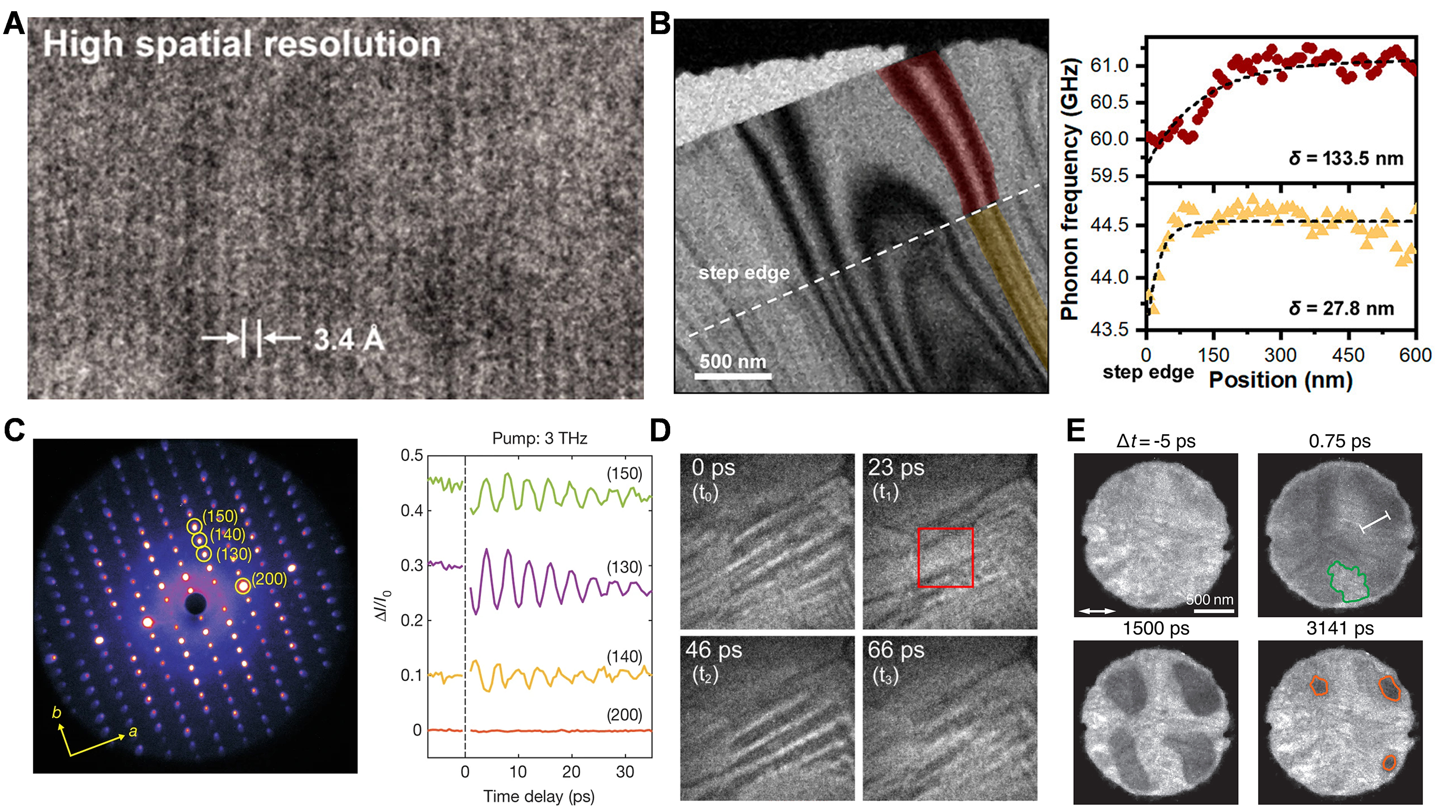
Figure 3. (A) High-resolution UTEM image of graphite with lattice-plane spacing of 3.4 Å. Reprinted with permission[48]. Copyright 2010, AAAS. (B) Representative UTEM image of a freestanding 2H-MoS2 flake with highlighted regions of interest (ROIs) from which phonon dynamics were mapped, and position-dependent phonon frequency in each ROI. Reprinted with permission[52]. Copyright 2021, American Chemical Society. (C) Measured diffraction pattern of WTe2 at equilibrium and changes in Bragg peak intensity as a function of time delay between terahertz pump pulses and the electron beam. Reprinted with permission[67]. Copyright 2019, Springer Nature. (D) Laser-induced martensitic transition and nucleation in the shape memory alloy MnNiSn detected by bright-field imaging. Reprinted with permission[81]. Copyright 2017, American Physical Society. (E) Laser-induced charge-density wave phase transition in 1T-TaS2 captured by dark-field imaging. Reprinted with permission[56]. Copyright 2021, AAAS.
UTEM with fs time resolution provides a unique means to capture phonon transport processes in nanomaterials, enabling the tracking of coherent phonon dynamics under pulsed laser excitation and the study of how nanostructures influence phonon nucleation and propagation. For example, Zhang et al. systematically studied defect-mediated anisotropic phonon dynamics in molybdenum disulfide (MoS2) through direct real-space imaging at nanoscale spatial and ps temporal resolutions [Figure 3B][51-53]. Sie et al., using UED combined with terahertz optical pulse excitation, achieved sub-ps interlayer shear strain regulation in the Weyl semimetal WTe2 [Figure 3C][67]. This study revealed a symmetry-breaking mechanism driven by terahertz-frequency shear phonon modes, confirming its ability to induce topological phase transitions and modulate the spatial distribution of the Weyl points, offering new insights for the development of ultra-high-speed topological electronic devices.
UTEM also plays a significant role in studying photoinduced phase transitions[93,94], such as crystal melting[95], nucleation and growth processes[96-98], lattice distortions in perovskite materials[18,99,100], and charge density wave (CDW) phase transitions[101-105], all of which have been extensively investigated. Unlike ensemble-averaged optical probes or reciprocal-space-only diffraction techniques, UTEM captures the heterogeneous nature of these transitions by enabling direct, real-space visualization of nucleation, domain growth, and interfacial propagation with simultaneous nanometer spatial and femtosecond temporal resolution. For example, Zhang et al. studied the photoinduced martensitic phase transition and its reverse process in the shape memory alloy Mn-Ni-Sn using ultrafast bright-field imaging [Figure 3D][81]. The study captured the periodic annihilation and regeneration of domain structures (period of ~40 ps), revealing the coupling mechanism between lattice breathing oscillations and phase transitions. This clarified the atomic motion patterns involved in twin nucleation and domain wall growth, providing an in situ dynamic observation method for studying symmetry-breaking phase transitions.
In CDW systems, UTEM has provided unprecedented insights into the spatiotemporal evolution of ordered states[56]. Compared to ultrafast bright-field imaging (UBF), ultrafast dark-field imaging (UDF) can acquire crystal structure information with higher contrast. Danz et al. employed a customized dark-field aperture array to simultaneously track the evolution of CDW domains with fs time resolution and 5 nm spatial resolution, elucidating relaxation pathways and domain wall dynamics in 1T-TaS2 [Figure 3E][56]. Their work revealed that domain wall dynamics, rather than uniform lattice melting, dominate the photoinduced disordering pathway. Through real-time, real-space imaging of the formation, stabilization, and relaxation processes of CDW domains, this study provided direct structural evidence for the phase transition mechanism following photoexcitation. Furthermore, UTEM has enabled the direct observation of topological defect formation during CDW transitions, such as phase slips and dislocations, which are critical for understanding the collective response of correlated electron systems to ultrafast excitation.
Owing to significant advances in in situ TEM technology, the implementation of multi-field conditions within TEM has become increasingly feasible. The integration of in situ specimen holder technology with UTEM has substantially expanded its scope for dynamic investigations[106], enabling the application of electric fields, magnetic fields, stress fields, heating/cooling, and various gas or liquid environmental conditions to characterize material properties and dynamic responses at nm or even atomic resolution[107,108]. For example, UTEM can directly observe photoinduced nucleation dynamics in water at nanoscale using in situ liquid cells, providing insights into reaction mechanisms, particularly the coupling between lattice vibrations and carrier dynamics[87]. Fu et al. [Figure 4A] achieved significant progress by integrating a liquid cell into UTEM to study the active Brownian dynamics of nanoparticles in water triggered by laser pulses[109]. On nm and ns scales, they observed unidirectional ultrafast ballistic motion of photon-activated gold nanoparticles along the liquid-gas interface[87]. These studies have successfully extended the application of UTEM to non-equilibrium fluid- and gas-phase reaction systems through the development of customized sample environments and pulse-control imaging techniques, offering atomic-scale dynamic perspectives for ultrafast processes in fields such as photocatalysis and energy conversion.
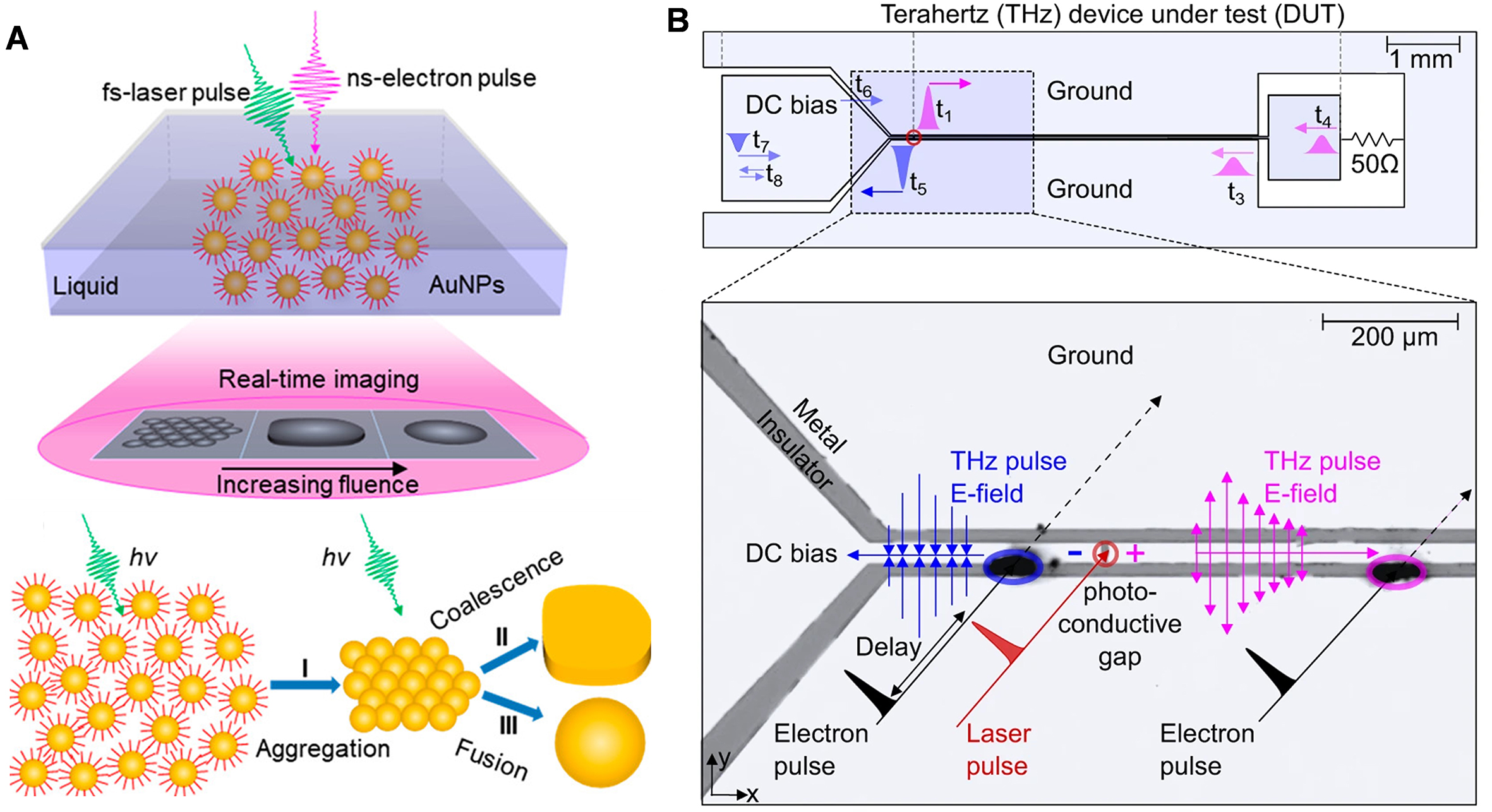
Figure 4. (A) Schematic illustration of real-time imaging of photomorphic reaction dynamics of Au nanoparticles in liquid by 4D-EM. Reprinted with permission[109]. Copyright 2018, American Chemical Society. (B) Schematics of the terahertz electronics device under test and optical microscope image of the active region. Reprinted with permission[110]. Copyright 2024, Springer Nature.
By applying electric fields to samples inside the TEM, researchers can observe field-induced phenomena such as electrochemical reactions[111], polarization[112], magnetization[113], and electromechanical responses[114]. Mattes et al. demonstrated that ultrafast electron-beam probes with terahertz-compressed electron pulses can directly sense local electromagnetic fields in electronic devices, achieving fs temporal, micrometer spatial, and millivolt signal resolutions [Figure 4B][110]. UTEM uniquely enables the visualization of atomic responses and carrier dynamics under electric fields, making it a powerful tool for investigating electronic and structural dynamics in nanoscale devices.
Ultrafast magnetic dynamics: lorentz TEM
Magnetic materials hold broad application prospects in fields such as data storage[115], logic operations[116-118], and quantum computing[119-121]. At the fundamental research level, the origin of magnetism is often closely related to interactions between spins or orbitals within materials and is frequently coupled with other order parameters, such as superconductivity, ferroelectricity, and CDW. Therefore, studying the temporal evolution of magnetic structures at the nanoscale and on the ultrafast timescales is crucial for understanding the nature of magnetism and its dynamic behavior. This not only helps reveal the complex coupling mechanisms among multiple order parameters in strongly correlated electron systems, but also lays the scientific foundation for designing and optimizing future novel spintronic functional devices.
Electron beams serve as an important means for magnetic probing at nanoscale. Although traditional optical-based pump-probe techniques have made great progress in studying ultrafast magnetic dynamics, their spatial resolution is limited by the optical diffraction limit, making it difficult to fully resolve transient evolution details of complex magnetic structures[122]. In contrast, electron beams, with their shorter de Broglie wavelengths and unique scattering mechanisms, can provide higher spatial resolution, making them a powerful tool for studying nanomagnetic dynamic processes. In recent years, the rapid development of ultrafast Lorentz TEM (ULTEM) technology has significantly enhanced comprehensive observation capabilities of magnetic materials across both time and space dimensions[123,124]. This technology combines fs laser pumping with electron beam probing, achieving fs time resolution and nm spatial resolution, thereby enabling direct imaging of the dynamic evolution of magnetic structures under non-equilibrium conditions[125]. Unlike ensemble-averaged optical probes, ULTEM captures the heterogeneous and nanoscale nature of magnetic dynamics, revealing how magnetic vortices, skyrmions, and domain walls nucleate, propagate, and interact under external stimuli. This capability provides direct access to key kinetic processes such as ultrafast demagnetization, spin-lattice relaxation, gyrotropic motion, and topological switching, which are essential for understanding fundamental spin dynamics and for developing next-generation spintronic devices.
The first ULTEM system was demonstrated by the Ahmed H. Zewail group, in which the magnetization reversal and domain wall motion dynamics in ferromagnetic thin films were successfully observed using time-resolved Fresnel imaging mode[126]. In recent years, with technological advancements, studies utilizing ULTEM to investigate the ultrafast dynamic evolution of magnetic structures at the nanoscale have increased. For example, Rubiano et al. employed fs Lorentz microscopy to probe the magnetic evolution during photoinduced demagnetization process in magnetic vortex structures[127]. This work achieved direct imaging of the ultrafast demagnetization process in a single nanostructure with a spatial resolution better than 100 nm and a temporal resolution as high as 700 fs [Figure 5A], demonstrating the potential of this technique for real-space imaging of nanoscale spin systems under ultrafast optical field excitation[127].
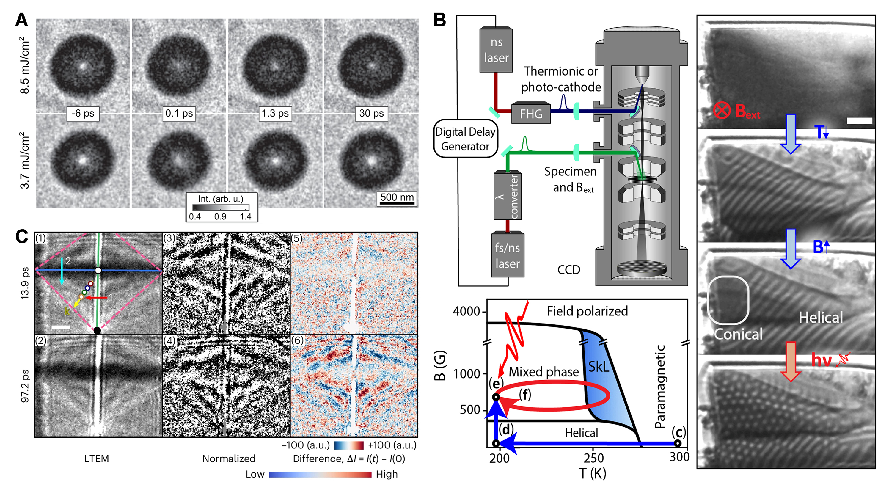
Figure 5. (A) Demagnetization process of a magnetic vortex observed by ultrafast LTEM. Reprinted with permission[127]. Copyright 2018, American Physical Society. (B) Schematic diagram of the light-induced generation process of a skyrmion. Top left: Schematic of the in-situ pump-probe cryogenic ultrafast LTEM experimental setup. Bottom left: Magnetic phase diagram of the FeGe nanoplates, arrows indicate key pathways within the phase diagram. Right: LTEM images of FeGe nanoplates under different conditions. The skyrmion lattice was generated by near-infrared fs laser pulses. Scale bar: 250 nm. Reprinted with permission[128]. Copyright 2018, American Physical Society. (C)Time-resolved ultrafast LTEM imaging of spin waves. Ultrafast LTEM images ((1) and (2)), intensity-normalized (to the averaged intensity by pixel) images ((3) and (4)), and difference images ((5) and (6)) at 13.7 ps ((1), (3) and (5)) and 97.2 ps ((2), (4) and (6)) delay times; Scale bar, 500 nm. Stripe-like contrast represents the spin-wave wavefronts. Reprinted with permission[129]. Copyright 2025, Springer Nature.
In the FeGe material system, low-temperature ns time-resolved ULTEM experiments showed that photoinduced thermal pulses of different durations and energies can enable controllable writing of magnetic skyrmions over a wide range of temperatures and magnetic fields [Figure 5B]. The study combined high-speed camera imaging and pump-probe techniques to directly resolve the spatiotemporal evolution path of the magnetic structure after laser pulse excitation. Results indicated that following the laser-induced demagnetization, the skyrmion lattice can maintain its structural integrity and recover to its initial state on sub-microsecond to microsecond timescales as the system cools. This study also successfully demonstrated the laser writing and erasing of magnetic skyrmions, systematically revealing their stability and dynamic evolution under different temperature and external magnetic field conditions[128]. Separately, Liu et al. at Brookhaven National Laboratory employed a laser-free ULTEM technique and reported a breakthrough in direct imaging of dipolar-exchange spin waves in ferromagnetic thin films. Leveraging topological spin textures, they captured the emission, propagation, reflection, and interference of spin waves from spin-antivortices under RF excitation [Figure 5C][129]. Their study revealed that spin wave generation is closely associated with the oscillatory motion of specific magnetic domain walls. ULTEM also facilitates the realization of skyrmions in two-dimensional van der Waals ferromagnets at room temperature and enables the exploration of their ultrafast laser writability, laying the foundation for future spintronic device applications. In experiments, Li et al. introduced iron deficiency into FeGaTe2 to break the crystal symmetry and induce a significant Dzyaloshinskii-Moriya interaction (DMI), thereby stabilizing Néel-type skyrmions at room temperature[130]. ULTEM also serves as an important tool for studying multi-scale skyrmion dynamics. For example, using ULTEM imaging, researchers systematically observed dynamic behaviors such as skyrmion proliferation, drift, contraction, and merging on ns to microsecond timescales in Co9Zn9Mn2, providing deep insights into their complex spatiotemporal evolution paths[72].
Therefore, ULTEM provides a powerful technique for studying the ultrafast dynamics of nanoscale magnetic structures, significantly advancing the understanding of the dynamic behavior of complex spin structures in magnetic materials. The aforementioned studies fully demonstrate the unique capability of ULTEM to reveal the dynamic response of topological spin structures under external field control with unprecedented spatiotemporal resolution. With its unparalleled spatiotemporal resolution, ULTEM has become an indispensable and distinctive tool for studying the microscopic dynamics of magnetic structures, particularly the nanoscale topological spin structures with potential applications in spintronic devices.
Multidimensional strain mapping: 5D-STEM
5D-STEM is a cutting-edge method that combines scanning transmission electron microscopy (STEM) with ultrafast optical pump-probe technology to achieve ultrafast dynamic mapping of lattice, charge, spin, and other physical properties in nanomaterials. Its core principle lies in using ultrashort electron pulses to perform a two-dimensional real-space scan of the sample while recording the complete electron diffraction pattern or electron beam deflection signal at each scan point, thereby simultaneously acquiring 5D information: real-space coordinates (x, y), time (t), and momentum space (kx, ky) [Figure 6A][50]. This approach differs from conventional STEM by replacing the static illumination with a converged electron probe and time-resolved detection, enabling the reconstruction of transient structural dynamics with both high spatial and temporal resolution[131].
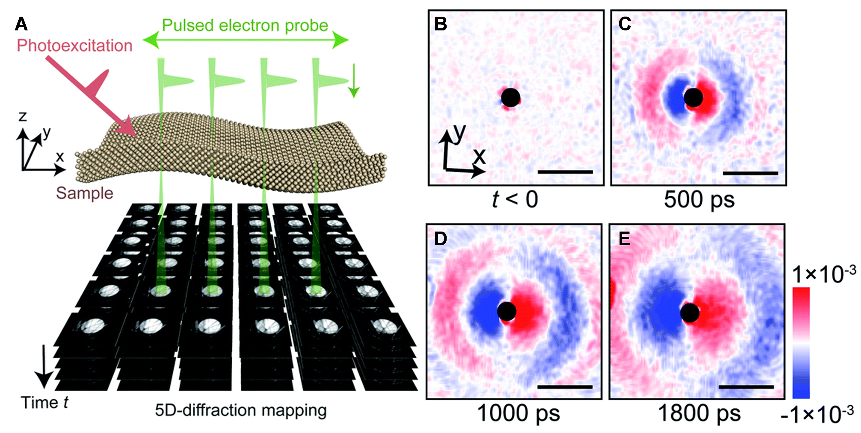
Figure 6. (A) Schematic of the 5D-STEM imaging technique. Reprinted with permission[50]. Copyright 2022, Royal Society of Chemistry. (B-E) Snapshots of coherent acoustic phonon propagation captured by 5D-STEM technique in a silicon thin film. Reprinted with permission[50]. Copyright 2022, Royal Society of Chemistry.
5D-STEM is an innovative characterization technique capable of observing the ultrafast dynamic behavior of nanomaterials with extremely high spatiotemporal resolution. The development of this technique can be traced back to 2009, when Yurtsever et al. first introduced the related concept. They employed convergent beam electron diffraction (CBED) to observe acoustic wave propagation in silicon, achieving an UTEM study of single-particle structural dynamics at the nanoscale[132]. Unlike traditional parallel-beam illumination with a single electron wavevector, this approach utilized a convergent electron beam to probe the sample, enabling high-precision determination of the three-dimensional structure of localized regions. Subsequently, Claus Ropers' team further advanced ultrafast CBED (U-CBED) to investigate photoinduced strain dynamics in nanostructures[133]. In 2022, Nakamura et al. upgraded U-CBED to 5D-STEM[50], realizing quantitative time-resolved mapping of strain at the nanoscale [Figure 6B-E][50]. Their work captured the generation and propagation of photoinduced acoustic waves in a nanostructured silicon thin plate. Through CBED analysis at each scanning pixel, they quantitatively determined the polarization direction and amplitude of the acoustic waves propagating along the plate and used Fourier transforms to reveal the strain distribution in momentum-frequency space, thereby obtaining the phonon dispersion relation along any in-plane direction.
These developments underscore the unique capabilities of 5D-STEM. Compared to conventional STEM, 5D-STEM can capture transient changes in the crystal structure, local strain, phase transitions, and domain configurations of nanomaterials under ultrafast photoexcitation, enabling quantitative nanoscale mapping of time-dependent strain fields [Figure 6B-E][50]. This capability is crucial for investigating ultrafast optically controlled strain and the generation and propagation of acoustic waves within nanostructures. The analytical approach is highly flexible and applicable to complex nanostructured samples. Beyond strain dynamics, 5D-STEM can also be utilized to study other types of ultrafast non-equilibrium phenomena, including structural phase transitions, dielectric responses, and magnetic dynamics. In the future, continuous improvements in the core components such as electron source brightness, detector speed, and synchronization control systems are expected to further enhance the spatiotemporal resolution and detection sensitivity of 5D-STEM.
Ultrafast electronic dynamics: time-resolved EELS
EELS in UTEM is a powerful tool for probing electronic dynamics because it uniquely combines high energy resolution with nanometer spatial and femtosecond temporal resolution, enabling direct observation of transient electronic states with element-specific sensitivity. Unlike optical spectroscopies that often average over ensemble responses and lack direct chemical specificity, time-resolved EELS analyzes core-level excitation edges and their time-dependent shifts, allowing researchers to distinguish between different chemical species, oxidation states, and charge states as they evolve following photoexcitation. With energy resolutions on the order of subelectronvolts and detection ranges spanning from a few electron volts to hundreds of electron volts, ultrafast EELS achieves temporal resolution reaching the femtosecond scale while preserving nanoscale spatial resolution, making it applicable to a wide range of studies from collective electron oscillations to core electron dynamics.
In addition to the structural dynamic characterization techniques mentioned above, multifunctional UTEM equipped with an electron energy loss spectrometer can be employed to reveal the electronic dynamics of materials through time-resolved EELS. Dynamic multimodal probing of lattice and electronic systems in advanced materials is a powerful approach for decoupling interactions among various degrees of freedom, which often give rise to novel equilibrium and transient properties in materials[134-136].
In the study of transition metal oxides, Carbone et al., utilizing spectral features near the Fe L3 edge in EELS, successfully distinguished between Fe4+ and O- hole states in the hematite[137]. They found that the lifetime of Fe4+ holes (a few picoseconds) was much shorter than that of O- holes, thereby explaining the differences in the photocatalytic performance of hematite under different illumination conditions from an atomic scale and demonstrating the potential for element-selective studies of charge dynamics [Figure 7A][137]. Time-resolved EELS has been particularly powerful for investigating coupled electronic and lattice dynamics in carbon-based materials. For instance, coherent phonons generated in graphite after photoexcitation cause periodic contraction and expansion of the c-axis lattice. This process, by influencing the chemical bonding state, directly leads to dynamic changes in the intensity and position of the plasmon peak in the EELS spectrum [Figure 7B][138] In one-dimensional materials such as single-walled carbon nanotubes, time-resolved EELS has observed dynamic processes where the π and π + σ plasmon peaks exhibit maximum red shift at approximately 1 ps delay and subsequently undergo a slow partial recovery [Figure 7C][139]. Combined with the Drude model, this result clearly attributes the rapid lattice expansion within ~1.4 ps to laser-induced valence band electron excitation, while associating subsequent processes with energy transfer from the electronic system to the lattice, thereby successfully distinguishing the electron-driven and phonon-driven lattice dynamics[139]. Similar plasmon dynamics have also been observed in boron nitride nanotubes, where energy bandgap contraction following photoexcitation has been quantitatively linked to lattice expansion[140]. These insights into electronic dynamics, particularly the competition between carrier recombination, trapping, and extraction are essential for understanding fundamental processes in energy conversion, quantum materials, photocatalysis, and for guiding the rational design of functional devices.
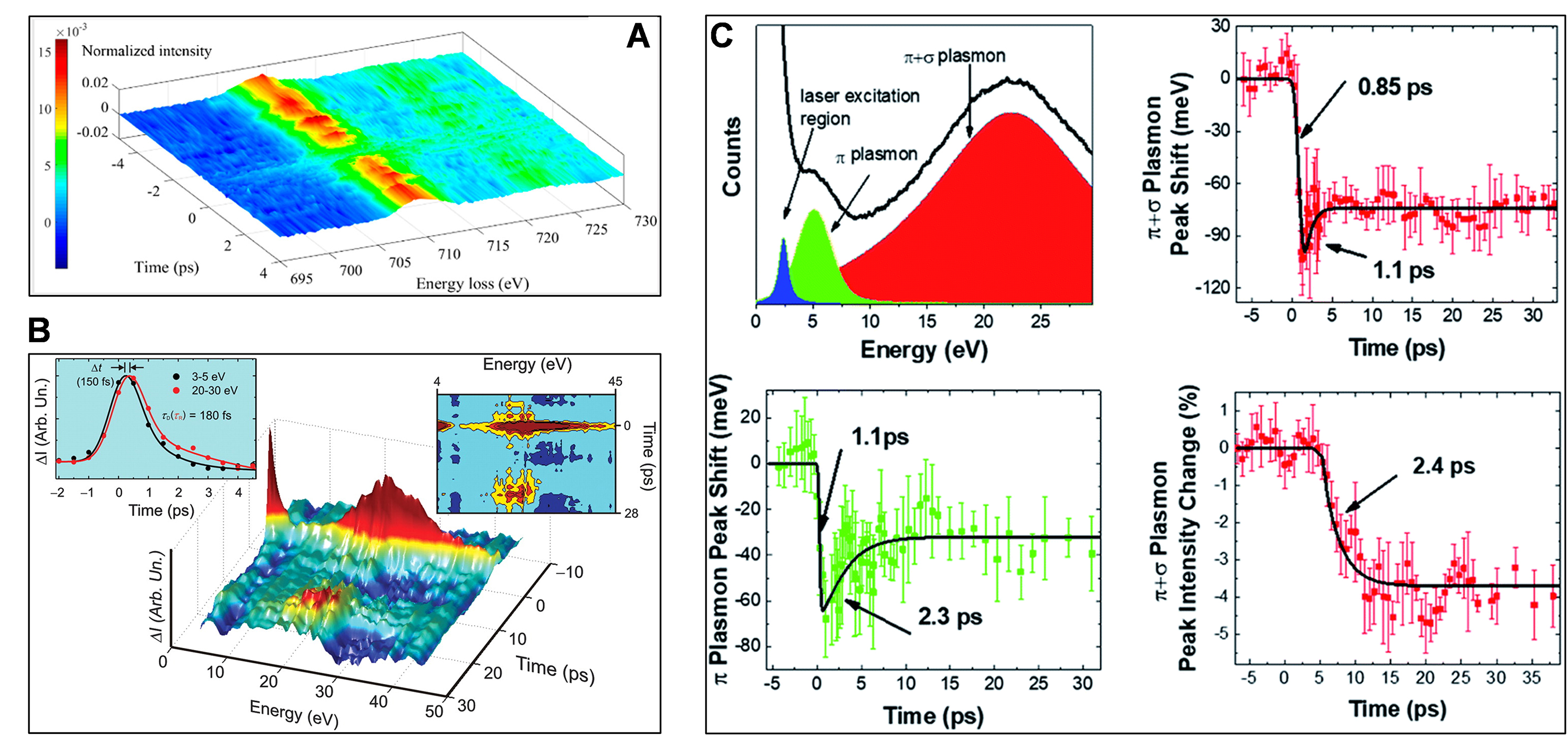
Figure 7. Ultrafast EELS and elemental valence analysis. (A) 3D intensity-energy-time EELS plot for graphite, showing the time-energy-amplitude evolution of the spectral changes at different time delays. Reprinted with permission[137]. Copyright 2009, AAAS. (B) 3D intensity-energy-time dynamics of the overall Fe L-edge EELS. Reprinted with permission[138]. Copyright 2017, American Chemical Society. (C) fs EELS of single-walled carbon nanotubes. Reprinted with permission[139]. (C) is reproduced under the CC BY-NC license.Copyright 2020, Royal Society of Chemistry.
Light-matter interactions: PINEM
PINEM is an important derivative technique in the UTEM, which enables to capture light-matter interactions as they unfold at nm and fs spatiotemporal resolution. In this technique, fs laser pulses excite the sample and create optical near-fields such as surface plasmons or phonon polaritons. As the electron beam transmits through these localized fields, inelastic interactions between the electrons and incident photons shift the electrons’ energy by discrete amounts. Mapping these shifts with electron energy loss spectroscopy or energy-filtered imaging then reveals the hidden landscape of the sample’s optical near-field, tracing its spatial pattern and ultrafast evolution in real time.
While optical near-field microscopy in materials science and biology breaks the diffraction limit, its spatial resolution still cannot match the atomic-scale of electron microscopy. When researchers need to track evanescent electromagnetic fields evolving over fs and at nm or even atomic level, ultrashort electron pulses offer a powerful solution. This approach builds on the basic physics of electron-photon interaction.
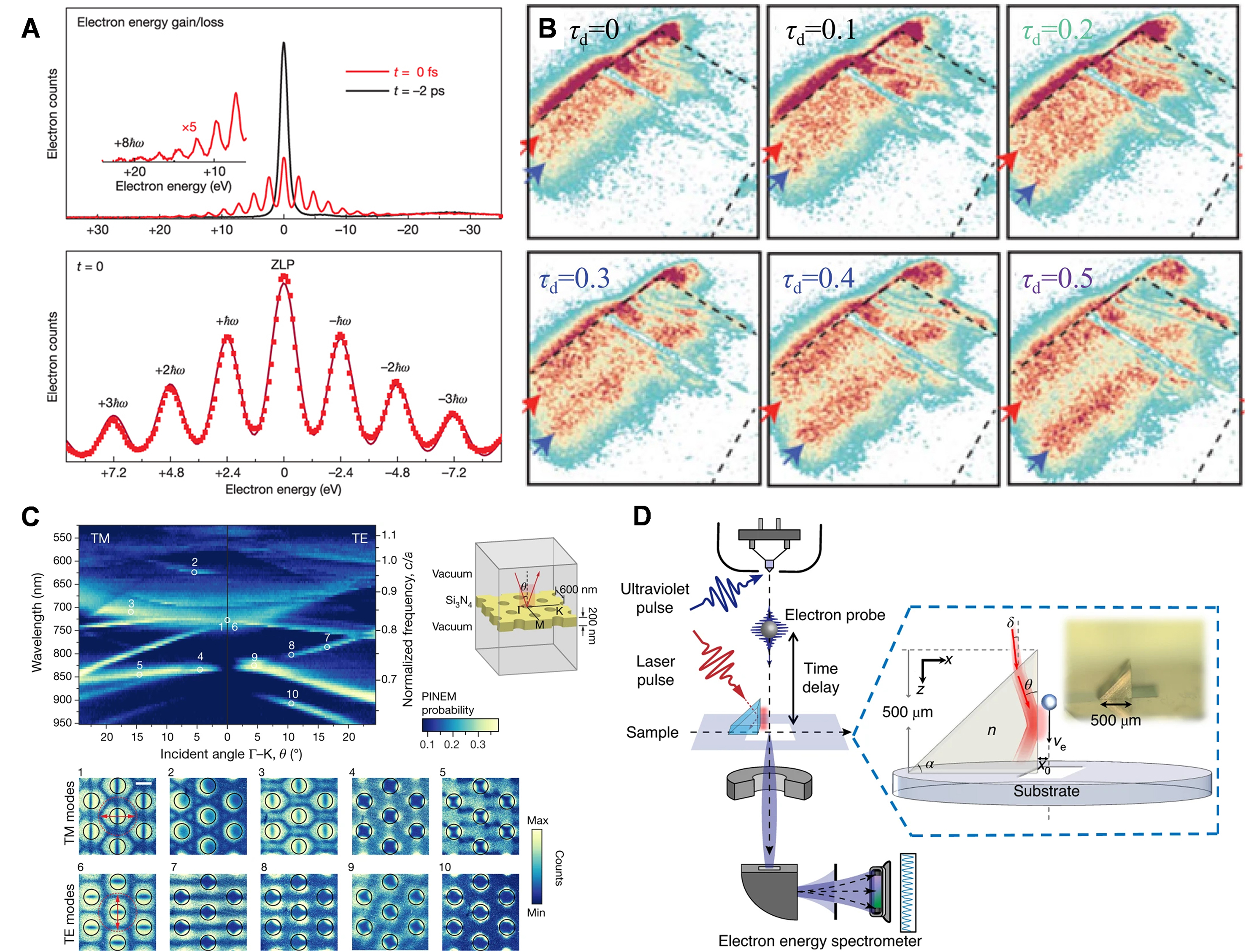
Figure 8. Electron-photon interaction and quantum control in UTEM. (A) Electron energy spectra for interaction with and without photons. Reprinted with permission[141]. Copyright 2009, Springer Nature. (B) Ultrafast PINEM imaging of phonon-polariton in hBN. Reprinted with permission[150]. Copyright 2021, AAAS. (C) PINEM imaging of electron interaction with optical Bloch mode inside photonic crystals. Reprinted with permission[155]. Copyright 2020, Springer Nature. (D) Resonant phase-matching between a light wave and a free-electron wavefunction. Reprinted with permission[157]. Copyright 2020, Springer Nature.
As an ultrafast near-field imaging method, PINEM has been widely applied to the study of ultrafast near-field dynamics in physics, chemistry, materials science, and biology, providing high-contrast images with nm-fs resolution[142-145]. Compared to bright-field TEM imaging, PINEM can effectively enhance the imaging of structures with weak scattering contrast, such as protein vesicles[146], organelles[147], and graphene step edges[148], because near-field enhancement effects are pronounced at the boundaries of these structures. Simultaneously, the high spatiotemporal resolution of PINEM makes it well-suited for investigating the generation, propagation, and decay dynamics of various polaritons (e.g., plasmons, phonon polaritons), including surface plasmon skyrmions in gold films[149] and phonon polaritons in hexagonal boron nitride [Figure 8B][150]. It can directly capture their dynamic behavior, measure group velocities, determine dispersion relations, and explore nonlinear optical phenomena within them. By incorporating a non-collinear optical parametric amplifier (NOPA) or OPA to tune the pump laser wavelength, PINEM can probe polaritons of different energies across the visible to far-infrared spectrum with meV-level energy resolution[151]. Compared to time-resolved photoemission electron microscopy (TR-PEEM) and scanning near-field optical microscopy (TR-SNOM), PINEM can investigate polariton behavior at buried interfaces, avoiding potential probe-induced interference with intrinsic near-field signals that may occur in SNOM, thereby offering a non-invasive detection approach[152].
The free-electron-photon interaction is essentially a quantum coherent phase modulation of the electron wavefunction, offering new avenues for controlling electron wavepackets on attosecond scales[153]. Researchers have successfully achieved strong longitudinal and transverse phase control of electron wavepackets, demonstrating light-driven Ramsey-type interferometry, multi-color interactions, nonlinear interactions, and even the generation of electron vortex beams[154]. Coherently shaped electron beams hold promise for applications in quantum measurements with atomic precision, phase-contrast imaging, and electron-optical aberration correction[49]. To enhance the strength of free-electron-photon interaction, optical resonators are widely used to improve light-field localization and light-matter coupling efficiency. In 2020, Wang et al. and Kfir et al. significantly enhanced electron-photon coupling strength by employing the optical Bloch modes of photonic crystals [Figure 8C][155] and the whispering-gallery modes of dielectric microsphere cavities[156], respectively. Besides increasing light-field intensity, extending the interaction distance between electrons and the light field under phase-matching conditions can also effectively improve the coupling efficiency. Dahan et al. utilized evanescent light fields generated by total internal reflection to interact with the electron beam, obtaining an electron-energy-comb spectrum with a bandwidth exceeding 1,700 eV [Figure 8D][157].
By synergistically increasing light-field intensity and interaction distance, schemes based on integrated photonic structures and dielectric laser accelerators have achieved effective manipulation of continuous electron beams. Recently, several technical routes have been proposed to attain attosecond time-resolved electron microscopy. Theoretical analyzes and experiments indicate that after interacting with a light field, probe electron pulses can be modulated into attosecond electron pulse trains after propagating a certain distance in the UTEM[158]. For instance, Nabben et al. modulated a continuous electron beam into attosecond-width pulses using a continuous-wave laser and pumped the sample with a second continuous laser, recording the optical response with an imaging energy filter[159]. However, because the pump source is a continuous laser, this method only provides dynamic information relative to a sub optical cycle.
Combining photon gating with PINEM is another effective approach for improving UTEM temporal resolution. By implementing two-color ultrafast pump-probe PINEM scheme based on free-electron-photon interaction, Fu et al. substantially enhanced the UTEM temporal resolution using an optical gating pulse of ~50 fs[160]. This scheme uses the 50-fs laser pulse interacting with the electron pulse at the sample position as a “time gate” to generate PINEM probe electron pulse with a width of ~50 fs, thereby improving the temporal resolution of UTEM by an order of magnitude. Using this approach, they successfully revealed the ultrafast dielectric-response dynamics of the insulator-to-metal phase transition in individual Mott-insulator VO2 nanowires at ~50 fs and few-nm spatiotemporal scales, demonstrating the great potential of PINEM in resolving physical processes at extreme spatiotemporal resolution. Moreover, Hui et al. utilized polarization gating to generate optical gating pulses with a width of ~625 as, achieving attosecond electron diffraction of photoinduced electron dynamics in multilayer graphene[161].
PINEM technology provides diverse means for precisely controlling free electrons by flexibly adjusting laser field strength, polarization, pulse width, phase, orbital angular momentum, and spatial distribution, enabling dynamic imaging of optical near-fields (such as various polaritons) at fs-nm scales. The application of PINEM has also recently extended beyond traditional UTEM, successfully reaching low-energy electron-photon interaction studies in scanning electron microscopy (SEM) and point-projection microscopy[162]. We believe that the photon-induced near-field effects observed in UTEM have broad application prospects, including but not limited to: direct spatiotemporal imaging of localized electromagnetic fields at interfaces (e.g., transient electric-field distributions at metal-semiconductor interfaces or catalytic active sites); visualization of nanophotonics, plasmonics, and related phenomena (e.g., surface-plasmon propagation, coupling of photonic-crystal modes, and exciton dynamics in quantum dots). By integrating ultrafast optics with electron microscopy, PINEM provides a powerful tool with atomic-scale spatial resolution and fs-to-attosecond temporal resolution for studying light-matter interactions at the nanoscale, strongly driving breakthroughs in frontier fields such as nanophotonics and quantum materials. With continued technological innovation, its application boundaries are expected to further expand into broader cross-disciplinary research areas, such as extreme physical conditions and life sciences.
ATTOSECOND ELECTRON MICROSCOPY AND APPLICATIONS
Principles of AEM
Attosecond electron microscopy (AEM) is an emerging characterization technique that combines the nm-to-atomic spatial resolving power of electron microscopy with attosecond (10-18 s) temporal resolution. Its defining principle is to use the optical phase as an “internal clock” to coherently modulate free-electron wavefunctions and, via energy- and phase-resolved readout, probe sub-cycle electromagnetic responses and electron dynamics in both real space and reciprocal space. This approach overcomes the limitations of conventional pump-probe schemes that rely on mechanical delay stages, instead encoding temporal information directly into the electron energy spectrum via the interaction with precisely controlled optical fields.
The core workflow of AEM involves two sequential light-electron interactions. In the first stage, a continuous-wave or femtosecond laser modulates the electron wavefunction by imposing a periodic phase or energy shift through near-field interaction with a nanostructure or dielectric membrane. This modulation generates gain/loss sidebands in the electron energy spectrum spaced by the photon energy. During subsequent free-space propagation, vacuum dispersion converts this energy modulation into temporal bunching, producing attosecond electron pulse trains at a designed propagation distance. In the second stage, these attosecond probes interact with the optically excited sample. By scanning the relative delay between the optical excitation and the electron probe, and recording the position- and energy-dependent changes, AEM reconstructs the time-evolving near-field distribution with sub-cycle temporal precision. Advanced variants such as optical-gated AEM and free-electron homodyne detection further enhance the temporal resolution and enable phase-sensitive reconstruction of complex light-driven dynamics[161].
Technical milestones
Bridged by coherent free-electron-light interactions, a growing body of work has demonstrated that optical phase can be encoded into the electron wavefunction and converted, through dispersive propagation and temporal bunching, into an electron probe that advances electron microscopy from imaging static structures to interrogating sub-optical-cycle processes. For example, Feist et al. established coherent optical phase modulation of free-electron quantum states in an electron-microscopy beamline and pointed out that the resulting coherent superposition can evolve into attosecond electron pulse trains upon propagation, laying the conceptual and experimental foundation for AEM[16].
The uniqueness of AEM is its attempt to approach the extremes of both time and space within a single platform. By adopting the optical cycle as an intrinsic timing reference, AEM can map sub-cycle dynamics such as wavepacket acceleration, scattering-phase evolution, local field waveforms, and energy exchange through imaging, diffraction, or energy-resolved detection. As highlighted in Morimoto’s review[163], optical-frequency bunching can drive electron pulses well below the fs regime, and shorter modulation wavelengths (higher optical frequencies) generally favor shorter attainable electron pulse durations, providing a feasible engineering pathway toward attosecond timing in electron microscopy. Operationally, the core workflow of AEM is to “optically compress” a conventional TEM electron beam into an attosecond pulse train synchronized to the optical period, and then use this train, at a controlled delay, to sample the specimen within a single optical cycle. In a first interaction stage, a continuous-wave or fs laser drives a modulation membrane or a nanostructure near-field, imposing a periodic phase/energy (velocity) modulation on the passing electron wavefunction and generating gain/loss sidebands in the electron energy spectrum spaced by the photon energy. During subsequent free-space propagation, vacuum dispersion converts the velocity modulation into temporal bunching, namely, the electron components with different energies effectively “catch up” or “separate”, producing an attosecond pulse train at a designed propagation distance. The attosecond probe then undergoes a second interaction with the laser-driven near-field of the specimen. By scanning the relative delay between optical excitation and the electron probe and recording the position-dependent energy change, it is able to obtain field-cycle contrast and reconstructs the time-evolving near-field distribution. In practice, energy filtering and/or diffraction imaging converts the delay-dependent response into a readable spatial signal sequence, enabling light-cycle-resolved, movie-like imaging of sub-cycle dynamics.
The key milestones of AEM can be organized along a coherent progression, from quantum-coherent electron-light modulation and attosecond pulse-train formation to TEM-integrated attosecond metrology, sub-cycle imaging applications, interferometric amplitude/phase readout, and extensions toward structured electron wavefunctions. In 2015, Feist et al. reported near-field coupling in UTEM that revealed multilevel Rabi oscillations and “quantum walks”, and they explicitly established the propagation-based route from coherent modulation of pulsed electrons to attosecond temporal structure [Figure 9A][16]. Shortly thereafter, Priebe et al. advanced coherent control of free-electron quantum states using phase-locked optical near-field interactions and introduced SQUIRRELS tomography to reconstruct the electron density matrix and Wigner function, thereby integrating generation, characterization, and inversion within a unified framework[164]. In 2018, Morimoto et al.[165] extended these concepts to diffraction and microscopy with attosecond electron pulse trains, reporting characteristic bunch durations of 820 as and enabling precise phase delay-sensitive measurements in reciprocal space [Figure 9B]. In 2020, Ryabov et al. embedded attosecond metrology into a continuous-beam TEM by using continuous-wave laser modulation to form sub-optical-cycle electron pulse sequences, emphasizing a comparatively simple retrofit that does not rely on a fs electron source and can retain the original electron-source brightness [Figure 9C][158]. In 2023,
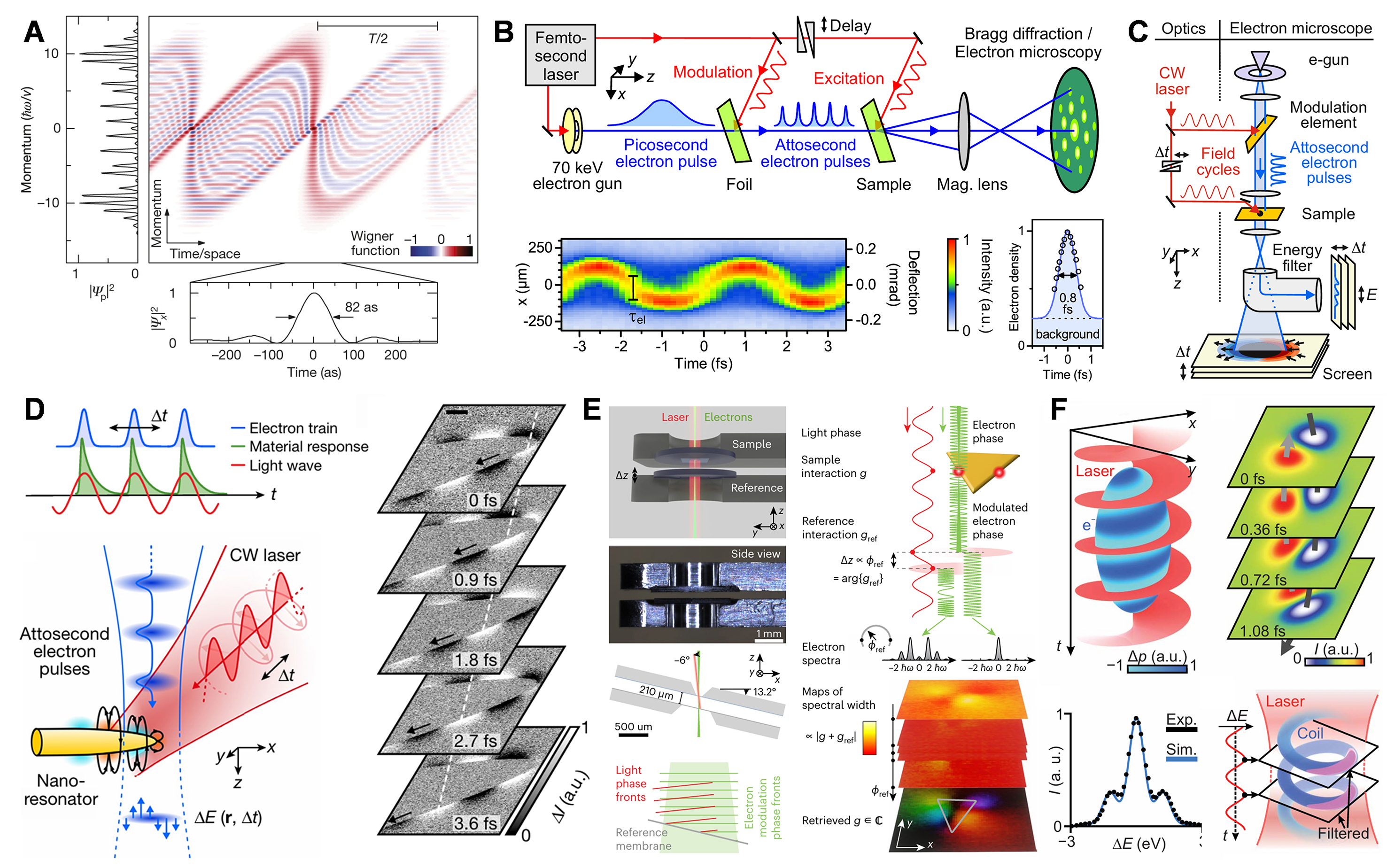
Figure 9. Development of AEM and representative applications. (A) Momentum projection of the Wigner function showing laser-induced spectral modulations. The temporal projection yields an 82 as (FWHM) peak in the laboratory frame. Reprinted with permission[16]. Copyright 2015, Springer Nature. (B) Generation and characterization of laser-compressed attosecond electron pulse trains at a dielectric foil. Attosecond streaking (deflect gram) and pulse retrieval give a 820 as (FWHM) peak above the background. Reprinted with permission[165]. Copyright 2018, Springer Nature. (C) Concept and experimental layout of attosecond-resolution electron microscopy. A laser-driven modulation stage produces attosecond electron pulses that probe the specimen at a controlled attosecond dela y. Reprinted with permission[158]. Copyright 2020, AAAS. (D) Light-cycle-resolved imaging within one optical cycle. Energy-change maps ΔE(r, Δt) provide field-cycle contrast and yield time-sequenced gain/loss images with nm-attosecond precision. Reprinted with permission[159]. Copyright 2023, Springer Nature. (E) High-spatial-resolution free-electron homodyne detection (FREHD). A focused beam traverses the sample and a vertically displaced reference membrane, and phase-controlled interferograms from raster-scanned spectra reconstruct the complex sample-induced phase modulation. Reprinted with permission[47]. Copyright 2024, AAAS. (F) Generation of attosecond electron coils. An optical vortex imprints a space-time-dependent momentum shift Δp to the electron wavepacket, then free-space propagation forms a chiral coil, and planar-wave attosecond gating with delay scanning enables 3D reconstruction. Reprinted with permission[166]. Copyright 2024, Springer Nature.
Potential applications
Taken together, AEM represents an ambitious shift in how we interrogate the microscopic world. It pushes temporal resolution toward the natural attosecond clock of matter while seeking to retain, and ultimately unify with, the atomic spatial resolution of electron microscopy. Decisive progress has already been achieved along the time axis, including the resolution of sub-cycle optical oscillations and landmark demonstrations in near-field imaging of nanophotonics. However, achieving robust atomic-resolution operation under attosecond conditions remains a central open challenge. At present, practical implementations typically operate from nm to sub-nm spatial resolution, and trade-offs between spatial and temporal performance define the current stage. Beyond near-fields in nanophotonics, the direct real-time observation of complex ultrafast chemical reactions and charge-transfer networks is still in a preparatory phase, limited by spatial resolution, sample damage, signal-to-noise, and reproducibility. Looking forward, essential progress is likely to rely on three coupled requirements: (i) improving contrast and suppressing background (e.g., via higher-order modulation-gating strategies, interferometric readout, or background-free bunching) to mitigate effective-current loss; (ii) strengthening stability and metrological rigor (phase locking, drift control, and systematic calibration) to move from proof-of-principle demonstrations to broadly usable quantitative tools; and (iii) developing microscope-compatible high-flux, high-coherence probes through deeper integration of on-chip nanophotonic structures with advanced computational microscopy and AI-enabled reconstruction, thereby increasing usable flux and inversion capability without sacrificing spatial resolution. Although commercialization remains distant and challenged by technical maturity, cost, and reliability, AEM is widely regarded as one of the ultimate techniques for ultrafast matter dynamics. Its transition from “producing attosecond electron structure” to “performing repeatable, invertible sub-cycle imaging in real materials and devices” will likely determine its paradigm-level impact across quantum materials, nanophotonics, photochemistry, and ultrafast energy conversion, with the potential to inspire disruptive advances in future information, energy, and materials technologies.
The potential applications of AEM span multiple frontiers in ultrafast science. In nanophotonics, AEM enables direct visualization of surface plasmon and phonon polariton dynamics with attosecond temporal and nanometer spatial resolution, revealing wave packet propagation, interference, and decay mechanisms that govern light-matter interactions at the nanoscale. In quantum materials, AEM can probe the ultrafast response of correlated electron systems, including charge density wave dynamics, metal-insulator transitions, and collective excitations such as plasmons and excitons, with the ability to resolve electronic motion on its natural timescale. In magnetism, attosecond electron pulses offer the potential to capture the fundamental timescale of demagnetization and spin dynamics, providing insights into spin-lattice interactions that are critical for spintronic applications. Furthermore, AEM holds promise for studying ultrafast chemical reactions and charge transfer processes at interfaces, where understanding electron dynamics on attosecond timescales is essential for controlling reaction pathways and improving energy conversion efficiencies. As the field continues to advance, AEM is poised to become a transformative tool for exploring the fastest dynamical processes in matter with unprecedented spatiotemporal precision.
OUTLOOK
Despite notable achievements, several challenges remain in UTEM: improving temporal resolution to the attosecond regime while maintaining atomic spatial resolution; enhancing in situ characterization under complex environments or external fields; and integrating multimodal probing to simultaneously measure structural, electronic, and magnetic dynamics. Addressing these requires interdisciplinary collaboration across electron optics, laser physics, computational science, and materials engineering.
Future UTEM development will focus on three key directions.
1. Hardware and electron sources. Attosecond electron sources will enable direct observation of electron wavepacket dynamics and sub-cycle light-matter interactions. Advances in photocathode materials (e.g., plasmonic and topological cathodes) promise brighter, more coherent electron pulses with reduced energy spread. Integration of on-chip nanophotonic structures offers a path toward compact, stable sources compatible with commercial platforms.
2. Methodology and data science. AI will play a central role across UTEM workflows. In experiment control, AI-driven real-time optimization will automate alignment, adaptive sampling, and region selection, accelerating acquisition and reducing damage. In data processing, machine learning, especially deep learning will enable intelligent denoising, feature extraction, and pattern recognition, converting multidimensional datasets (e.g., 5D-STEM, time-resolved EELS) into interpretable insights. AI-assisted inverse problem solving will bridge experimental observables with theoretical models. Combined with multimodal probing, these approaches will decouple coupled electronic, lattice, and spin dynamics in complex quantum materials.
3. Application expansion. Refined 5D-STEM methodologies will enable quantitative operando mapping of strain, charge, and lattice tilt. Advanced in situ holders (liquid, gas, cryogenic) will allow real-time observation under realistic conditions, such as battery reactions, catalysis, and biological processes. Coupling in situ capabilities with ultrafast time resolution will open new frontiers in operando characterization for energy storage, catalysis, and biomedicine.
Together, these advancements will position UTEM as a powerful tool for exploring ultrafast dynamic processes, driving paradigm shifts in materials design, energy conversion, and biomedicine.
CONCLUSIONS
By surpassing the spatiotemporal limits of conventional techniques, UTEM has become an indispensable tool for probing material dynamics from nanometer to atomic scales. Its ability to directly visualize transient processes, lattice dynamics, phase transitions, carrier transport, and magnetic switching has opened new avenues for understanding non-equilibrium phenomena. UTEM has evolved from early efforts focused on temporal resolution into a comprehensive platform integrating ultrahigh spatiotemporal resolution with multimodal, multi-parameter measurements. These capabilities have been applied to low-dimensional quantum materials, perovskite photovoltaics, topological insulators, and biological macromolecules.
Scientifically, UTEM has moved beyond phenomenological observation toward quantitative in situ investigations. Key studies have captured real-time lattice dynamics, ultrafast distortions in perovskites, laser-induced changes in liquid hydrogen-bond networks[167], and low-dose imaging of protein crystals[168], providing direct experimental evidence for ultrafast material responses. Technologically, innovations in electron pulse generation and manipulation remain central. The integration of femtosecond laser technology overcame temporal bottlenecks and enabled coherent control of electron wavepackets, propelling UTEM from “ultrafast imaging” to a versatile platform combining time-resolved diffraction, spectroscopy, in situ stimuli, and AI-assisted analysis.
Interdisciplinary impact is profound. In quantum materials, UTEM has visualized hidden phase transitions, charge density wave dynamics, and topological defects, offering insights into coupled electronic, lattice, and spin degrees of freedom. In energy conversion, it has revealed carrier relaxation, charge transfer, and lattice dynamics in perovskites and photocatalysts, directly informing strategies to improve charge separation and reduce recombination losses. In biomedicine, single- or few-electron pulses enable high-resolution, low-dose imaging of protein crystals and membrane proteins. Liquid-cell UTEM allows real-time observation of nanoparticle dynamics in physiological environments, shedding light on drug delivery and bio-nano interactions. Collectively, these applications demonstrate that UTEM is a transformative platform bridging fundamental science with quantum technologies, sustainable energy, and nanomedicine.
DECLARATIONS
Authors’ contributions
Conception, organization, and initial manuscript drafting: Liu, F.; Liu, J.
Conceived the work: Liu, F.; Liu, J.; Fu, X.
Organized the content and prepared the draft manuscript: Liu, F.; Liu, J.; Chen, L.; Tong, L.
Supervised the work: Fu, X.; Ji, S.
Revised the manuscript: Liu, F.; Liu, J.; Chen, L.; Tong, L.; Ji, S.; Fu, X.
All authors contributed to the writing and revision of the manuscript.
Availability of data and materials
Not applicable.
AI and AI-assisted tools statement
Not applicable.
Financial support and sponsorship
This project is supported by the National Key Research and Development Program of China (Grant Nos. 2024YFA1408000, 2023YFB3307700, 2023YFA1507000), National Natural Science Foundation of China (Grant Nos. 12127803, 92477130, 12427806, 12074195, 22573050), Nankai University 2025 Scientific Instrument Experimental Technology Research and Development Project (Grant No. 25NKSYJS05), 111 Project (Grant No. B23045), Fundamental Research Funds for the Central Universities, Nankai University (Grant Nos. 63213040, C029211101, C02922101, ZB22000104, DK2300010207, 63243194, 9242000728).
Conflicts of interest
Fu, X. is an Editorial Board Member of the journal Microstructures but is not involved in any steps of editorial processing, notably including reviewer selection, manuscript handling, or decision-making, while the other authors have declared that they have no conflicts of interest.
Ethical approval and consent to participate
Not applicable.
Consent for publication
Not applicable.
Copyright
© The Author(s) 2026.
REFERENCES
1. Li, J.; Wu, L.; Yang, S.; et al. Direct detection of V-V atom dimerization and rotation dynamic pathways upon ultrafast photoexcitation in VO2. Phys. Rev. X. 2022, 12, 021032.
2. Hervé, M.; Privault, G.; Zerdane, S.; et al. Multiscale phase nucleation driven by photoinduced polarons in a volume-changing material. Nat. Mater. 2026, 25, 588-94.
3. Sun, D.; Wu, Z.; Divin, C.; et al. Ultrafast relaxation of excited dirac fermions in epitaxial graphene using optical differential transmission spectroscopy. Phys. Rev. Lett. 2008, 101, 157402.
4. Pierret, A.; Loayza, J.; Berini, B.; et al. Excitonic recombinations in h-BN: from bulk to exfoliated layers. Phys. Rev. B. 2014, 89, 035414.
5. Wang, H.; Xiao, X.; An, Q.; et al. Low‐frequency evolution mechanism of customized HEAs‐based electromagnetic response modes manipulated by carbothermal shock. Small 2024, 20, 2309773.
6. Woutersen, S.; Emmerichs, U.; Bakker, H. J. Femtosecond Mid-IR pump-probe spectroscopy of liquid water: evidence for a two-component structure. Science 1997, 278, 658-60.
7. Schröder, A.; Wendeln, A.; Weber, J. T.; Mukai, M.; Kohno, Y.; Schäfer, S. Laser-driven cold field emission source for ultrafast transmission electron microscopy. Ultramicroscopy 2025, 275, 114158.
8. Aseyev, S. A.; Mironov, B. N.; Poydashev, D. G.; et al. High spatiotemporal resolution transmission electron microscopy and diffraction: progress from subnanosecond laser-induced structural dynamics to femtosecond quantum tomography. Nano. Today. 2025, 61, 102638.
9. Lobastov, V. A.; Srinivasan, R.; Zewail, A. H. Four-dimensional ultrafast electron microscopy. Proc. Natl. Acad. Sci. USA. 2005, 102, 7069-73.
10. Vogelsang, J.; Mikkelsen, A.; Ropers, C.; et al. Attosecond microscopy - advances and outlook. Europhys. Lett. 2025, 149, 36001.
11. Rehmann, J.; Röllin, M.; Vaterlaus, A.; Acremann, Y. Introducing ultrafast EBIC: spatially resolved transient analysis of an avalanche photodiode. Appl. Phys. Lett. 2025, 127, 203506.
12. Huang, Z.; Xie, X.; Guo, J.; et al. An ultrafast transmission electron microscopy with integration of transient optical spectroscopy. Adv. Sci. Instrum. 2026, 1, 100007.
13. Ji, S.; Guo, J.; Li, Z.; et al. Development of a femtosecond analytical electron microscopy based on a Schottky field emission transmission electron microscope. Rev. Sci. Instrum. 2025, 96, 033701.
14. Fu, X.; Wang, E.; Zhao, Y.; et al. Direct visualization of electromagnetic wave dynamics by laser-free ultrafast electron microscopy. Sci. Adv. 2020, 6, eabc3456.
15. Weßels, T.; Däster, S.; Murooka, Y.; et al. Continuous illumination picosecond imaging using a delay line detector in a transmission electron microscope. Ultramicroscopy 2022, 233, 113392.
16. Feist, A.; Echternkamp, K. E.; Schauss, J.; Yalunin, S. V.; Schäfer, S.; Ropers, C. Quantum coherent optical phase modulation in an ultrafast transmission electron microscope. Nature 2015, 521, 200-3.
17. Moradifar, P.; Liu, Y.; Shi, J.; et al. Accelerating quantum materials development with advances in transmission electron microscopy. Chem. Rev. 2023, 123, 12757-94.
18. Zhang, H.; Li, W.; Essman, J.; et al. Ultrafast relaxation of lattice distortion in two-dimensional perovskites. Nat. Phys. 2023, 19, 545-50.
19. Du, D. X.; Simjanoska, M.; Fitzpatrick, A. W. Four-dimensional microED of conformational dynamics in protein microcrystals on the femto-to-microsecond timescales. J. Struct. Biol. 2023, 215, 107941.
20. Liu, C.; Yang, K.; Zhang, J.; Cheng, S.; Shan, C. In-situ transmission electron microscopy shedding light on the mechanical properties of nanoscale materials. Microstructures 2024, 4, 2024055.
21. Jiang, T.; Pivak, Y.; Ni, F.; et al. Micro-electromechanical system-based cryogenic and heating in situ transmission electron microscopy for investigating phase transitions and domain evolution in single-crystal BaTiO3. Microstructures 2024, 4, 2024058.
22. Liang, H.; Zhou, Y.; Sun, S.; Liao, H. In situ liquid-phase transmission electron microscopy for electrocatalysis. Adv. Funct. Mater. 2025, 36, e13810.
23. Bostanjoglo, O.; Horinek, W. Pulsed TEM: a new method to detect transient structures in fast phase transitions. Optik 1983, 65, 361-7. Available from: https://www.scopus.com/pages/publications/0020843610 [Last accessed on 9 Jun 2026].
24. Lian, Y.; Sun, J.; Jiang, L. Probing electron and lattice dynamics by ultrafast electron microscopy: principles and applications. Int. Journal. Mech. Sys. Dyn. 2023, 3, 192-212.
25. Filippetto, D.; Musumeci, P.; Li, R.; et al. Ultrafast electron diffraction: visualizing dynamic states of matter. Rev. Mod. Phys. 2022, 94, 045004.
26. Wang, W.; Sun, S.; Li, J.; et al. Capturing the non-equilibrium state in light–matter–free-electron interactions through ultrafast transmission electron microscopy. Chinese. Phys. B. 2023, 33, 010701.
27. Yannai, M.; Kaminer, I. Emerging modalities for condensed matter explorations using ultrafast electron microscopy. Microsc. Microanal. 2024, 30, ozae044.720.
28. Lagrange, T.; Cattaneo, P.; Barwick, B.; Flannigan, D. J.; Weissenrieder, J.; Carbone, F. Laser-driven ultrafast transmission electron microscopy. Nat. Rev. Methods. Primers. 2025, 5, 61.
29. Hassan, M. T.; Baskin, J. S.; Liao, B.; Zewail, A. H. High-temporal-resolution electron microscopy for imaging ultrafast electron dynamics. Nat. Photonics. 2017, 11, 425-30.
30. Dömer, H.; Bostanjoglo, O. High-speed transmission electron microscope. Rev. Sci. Instrum. 2003, 74, 4369-72.
31. Lagrange, T.; Armstrong, M. R.; Boyden, K.; et al. Single-shot dynamic transmission electron microscopy. Appl. Phys. Lett. 2006, 89, 044105.
32. Bostanjoglo, O.; Rosin, T. Ultrasonically induced magnetic reversals observed by stroboscopic electron microscopy. Opt. Acta. Int. J. Opt. 2010, 24, 657-64.
33. Plows, G. S.; Nixon, W. C. Stroboscopic scanning electron microscopy. J. Phys. E. Sci. Instrum. 1968, 1, 595-600.
34. Montgomery, E.; Leonhardt, D.; Roehling, J. Ultrafast transmission electron microscopy: principles and applications. Front. Phys. 2026, 21, 032301.
35. Verhoeven, W.; Van Rens, J. F. M.; Kemper, A. H.; et al. Design and characterization of dielectric filled TM110 microwave cavities for ultrafast electron microscopy. Rev. Sci. Instrum. 2019, 90, 083703.
36. Lau, J. W.; Schliep, K. B.; Katz, M. B.; et al. Laser-free GHz stroboscopic transmission electron microscope: components, system integration, and practical considerations for pump-probe measurements. Rev. Sci. Instrum. 2020, 91, 021301.
37. Reisbick, S. A.; Han, M.; Liu, C.; et al. Stroboscopic ultrafast imaging using RF strip-lines in a commercial transmission electron microscope. Ultramicroscopy 2022, 235, 113497.
38. Qiu, J.; Ha, G.; Jing, C.; et al. GHz laser-free time-resolved transmission electron microscopy: a stroboscopic high-duty-cycle method. Ultramicroscopy 2016, 161, 130-6.
39. Aseyev, S.; Ryabov, E.; Mironov, B.; Ischenko, A. The development of ultrafast electron microscopy. Crystals 2020, 10, 452.
40. Houdellier, F.; Caruso, G.; Weber, S.; Kociak, M.; Arbouet, A. Development of a high brightness ultrafast Transmission Electron Microscope based on a laser-driven cold field emission source. Ultramicroscopy 2018, 186, 128-38.
41. Verhoeven, W.; Van Rens, J.; Kieft, E.; Mutsaers, P.; Luiten, O. High quality ultrafast transmission electron microscopy using resonant microwave cavities. Ultramicroscopy 2018, 188, 85-9.
42. Otto, M. R.; René, De. Cotret. L. P.; Stern, M. J.; Siwick, B. J. Solving the jitter problem in microwave compressed ultrafast electron diffraction instruments: robust sub-50 fs cavity-laser phase stabilization. Struct. Dyn. 2017, 4, 051101.
43. Sherlock, B.; Saint-jalm, S.; Malcolm, G. P. A.; Maker, G. T.; Moger, J. Ultra-low timing jitter, Ti:Al2O3 synchronization for stimulated Raman scattering and pump-probe microscopy. J. Biomed. Opt. 2020, 25, 1.
44. Huang, J. H.; Hu, X. Y. Overcoming residual timing jitter in pump-probe interferometry via weak value amplification and deep learning. arXiv 2025, arXiv:2511.12050.
45. Hassan, M. T.; Liu, H.; Baskin, J. S.; Zewail, A. H. Photon gating in four-dimensional ultrafast electron microscopy. Proc. Natl. Acad. Sci. USA. 2015, 112, 12944-9.
46. Zewail, A. H. 4D ultrafast electron diffraction, crystallography, and microscopy. Annu. Rev. Phys. Chem. 2006, 57, 65-103.
47. Gaida, J. H.; Lourenço-Martins, H.; Sivis, M.; et al. Attosecond electron microscopy by free-electron homodyne detection. Nat. Photonics. 2024, 18, 509-15.
49. Konečná, A.; De Abajo, F. J. G. Electron beam aberration correction using optical near fields. Phys. Rev. Lett. 2020, 125, 030801.
50. Nakamura, A.; Shimojima, T.; Ishizaka, K. Visualizing optically-induced strains by five-dimensional ultrafast electron microscopy. Faraday. Discuss. 2022, 237, 27-39.
51. Zhang, Y.; Flannigan, D. J. Observation of anisotropic strain-wave dynamics and few-layer dephasing in mos2 with ultrafast electron microscopy. Nano. Lett. 2019, 19, 8216-24.
52. Zhang, Y.; Flannigan, D. J. Imaging nanometer phonon softening at crystal surface steps with 4D ultrafast electron microscopy. Nano. Lett. 2021, 21, 7332-8.
53. Mckenna, A. J.; Eliason, J. K.; Flannigan, D. J. Spatiotemporal evolution of coherent elastic strain waves in a single MoS2 flake. Nano. Lett. 2017, 17, 3952-8.
54. Cremons, D. R.; Plemmons, D. A.; Flannigan, D. J. Femtosecond electron imaging of defect-modulated phonon dynamics. Nat. Commun. 2016, 7, 11230.
55. Li, J.; Qi, Y.; Yang, Q.; et al. Femtosecond electron diffraction reveals local disorder and local anharmonicity in thermoelectric SnSe. Adv. Mater. 2024, 36, 2313742.
56. Danz, T.; Domröse, T.; Ropers, C. Ultrafast nanoimaging of the order parameter in a structural phase transition. Science 2021, 371, 371-4.
57. Qi, Y.; Guan, M.; Zahn, D.; et al. Traversing double-well potential energy surfaces: photoinduced concurrent intralayer and interlayer structural transitions in XTe2 (X = Mo, W). ACS. Nano. 2022, 16, 11124-35.
58. Luo, D.; Zhang, B.; Sie, E. J.; et al. Ultrafast optomechanical strain in layered GeS. Nano. Lett. 2023, 23, 2287-94.
59. Eichberger, M.; Schäfer, H.; Krumova, M.; et al. Snapshots of cooperative atomic motions in the optical suppression of charge density waves. Nature 2010, 468, 799-802.
60. Erasmus, N.; Eichberger, M.; Haupt, K.; et al. Ultrafast dynamics of charge density waves in 4Hb-TaSe2 probed by femtosecond electron diffraction. Phys. Rev. Lett. 2012, 109, 167402.
61. Frigge, T.; Hafke, B.; Witte, T.; et al. Optically excited structural transition in atomic wires on surfaces at the quantum limit. Nature 2017, 544, 207-11.
62. Gao, M.; Lu, C.; Jean-Ruel, H.; et al. Mapping molecular motions leading to charge delocalization with ultrabright electrons. Nature 2013, 496, 343-6.
63. Möhr-Vorobeva, E.; Johnson, S. L.; Beaud, P.; et al. Nonthermal melting of a charge density wave in TiSe2. Phys. Rev. Lett. 2011, 107, 036403.
64. Van Der Veen, R. M.; Kwon, O.; Tissot, A.; Hauser, A.; Zewail, A. H. Single-nanoparticle phase transitions visualized by four-dimensional electron microscopy. Nat. Chem. 2013, 5, 395-402.
65. Kogar, A.; Zong, A.; Dolgirev, P. E.; et al. Light-induced charge density wave in LaTe3. Nat. Phys. 2019, 16, 159-63.
66. Horstmann, J. G.; Böckmann, H.; Wit, B.; Kurtz, F.; Storeck, G.; Ropers, C. Coherent control of a surface structural phase transition. Nature 2020, 583, 232-6.
67. Sie, E. J.; Nyby, C. M.; Pemmaraju, C. D.; et al. An ultrafast symmetry switch in a Weyl semimetal. Nature 2019, 565, 61-6.
68. Ji, S.; Grånäs, O.; Kumar Prasad, A.; Weissenrieder, J. Influence of strain on an ultrafast phase transition. Nanoscale 2023, 15, 304-12.
69. Cao, G.; Jiang, S.; Åkerman, J.; Weissenrieder, J. Femtosecond laser driven precessing magnetic gratings. Nanoscale 2021, 13, 3746-56.
70. Nagaosa, N.; Tokura, Y. Topological properties and dynamics of magnetic skyrmions. Nat. Nanotechnol. 2013, 8, 899-911.
72. Shimojima, T.; Nakamura, A.; Yu, X.; et al. Nano-to-micro spatiotemporal imaging of magnetic skyrmion’s life cycle. Sci. Adv. 2021, 7, eabg1322.
73. Möller, M.; Gaida, J. H.; Schäfer, S.; Ropers, C. Few-nm tracking of current-driven magnetic vortex orbits using ultrafast Lorentz microscopy. Commun. Phys. 2020, 3, 36.
74. Padmanabhan, H.; Stoica, V. A.; Kim, P. K.; et al. Large exchange coupling between localized spins and topological bands in MnBi2Te4. Adv. Mater. 2022, 34, 2202841.
75. Zheng, Q.; Tian, Y.; Shen, X.; et al. Fast attenuation of high-frequency acoustic waves in bicontinuous nanoporous gold. Appl. Phys. Lett. 2021, 119, 063101.
76. Wei, L.; Sun, S.; Guo, C.; et al. Dynamic diffraction effects and coherent breathing oscillations in ultrafast electron diffraction in layered 1T-TaSeTe. Struct. Dyn. 2017, 4, 044012.
77. Zhang, Y.; Sun, S.; Wang, W.; et al. Inhomogeneous excitation-regulated coherent strain wave in 2H-MoTe2 revealed by ultrafast electron microscopy. Phys. Rev. B. 2023, 108, 245426.
78. Zong, A.; Zhang, Q.; Zhou, F.; et al. Spin-mediated shear oscillators in a van der Waals antiferromagnet. Nature 2023, 620, 988-93.
79. Morrison, V. R.; Chatelain, R. P.; Tiwari, K. L.; et al. A photoinduced metal-like phase of monoclinic VO2 revealed by ultrafast electron diffraction. Science 2014, 346, 445-8.
80. Yang, D.; Baum, P.; Zewail, A. H. Ultrafast electron crystallography of the cooperative reaction path in vanadium dioxide. Struct. Dyn. 2016, 3, 034304.
81. Zhang, M.; Cao, G.; Tian, H.; et al. Picosecond view of a martensitic transition and nucleation in the shape memory alloy Mn50Ni40Sn10 by four-dimensional transmission electron microscopy. Phys. Rev. B. 2017, 96, 174203.
82. Xu, C.; Jin, C.; Chen, Z.; et al. Transient dynamics of the phase transition in VO2 revealed by mega-electron-volt ultrafast electron diffraction. Nat. Commun. 2023, 14, 1265.
83. Li, J.; Yue, L.; Chen, Z.; Xiang, D.; Cao, J. Photoinduced shortening of metallic bond in 1T′-ReS2 revealed by femtosecond electron diffraction. Appl. Phys. Lett. 2024, 124, 171905.
84. Britt, T. L.; Li, Q.; René De Cotret, L. P.; et al. Direct view of phonon dynamics in atomically thin MoS2. Nano. Lett. 2022, 22, 4718-24.
85. Iwasaki, Y.; Fukuda, T.; Noyama, G.; et al. Electronic intraband scattering in a transition-metal dichalcogenide observed by double-excitation ultrafast electron diffraction. Appl. Phys. Lett. 2023, 123, 181901.
86. Hu, J.; Xiang, Y.; Ferrari, B. M.; Scalise, E.; Vanacore, G. M. Indirect exciton-phonon dynamics in MoS2 revealed by ultrafast electron diffraction. Adv. Funct. Mater. 2023, 33, 2206395.
87. Fu, X.; Liu, S.; Chen, B.; Tang, J.; Zhu, Y. Observation and control of unidirectional ballistic dynamics of nanoparticles at a liquid-gas interface by 4D electron microscopy. ACS. Nano. 2021, 15, 6801-10.
88. Tauchert, S. R.; Volkov, M.; Ehberger, D.; et al. Polarized phonons carry angular momentum in ultrafast demagnetization. Nature 2022, 602, 73-7.
89. Duncan, C. J. R.; Johnson, A. C.; Maity, I.; et al. Photoinduced twist and untwist of moiré superlattices. Nature 2025, 647, 619-24.
90. Su, Y.; Zong, A.; Kogar, A.; et al. Delamination-assisted ultrafast wrinkle formation in a freestanding film. Nano. Lett. 2023, 23, 10772-8.
91. Kim, Y.; Lee, Y.; Kim, K.; Kwon, O. Light-induced anisotropic morphological dynamics of black phosphorus membranes visualized by dark-field ultrafast electron microscopy. ACS. Nano. 2020, 14, 11383-93.
93. Jelic, V.; Adams, S.; Maldonado-Lopez, D.; et al. Terahertz field control of surface topology probed with subatomic resolution. Nat. Photonics. 2025, 19, 1048-55.
94. Stoica, V. A.; Yang, T.; Das, S.; et al. Non-equilibrium pathways to emergent polar supertextures. Nat. Mater. 2024, 23, 1394-401.
95. Monti, M.; Siddiqui, K. M.; Perez-Salinas, D.; et al. Ultrafast surface melting of orbital order in La0.5Sr1.5MnO4. Nat. Mater. 2025, 25, 58-64.
96. Yoo, B.; Kwon, O.; Liu, H.; Tang, J.; Zewail, A. H. Observing in space and time the ephemeral nucleation of liquid-to-crystal phase transitions. Nat. Commun. 2015, 6, 8639.
97. Mo, M. Z.; Chen, Z.; Li, R. K.; et al. Heterogeneous to homogeneous melting transition visualized with ultrafast electron diffraction. Science 2018, 360, 1451-5.
98. Barwick, B.; Park, H. S.; Kwon, O.; Baskin, J. S.; Zewail, A. H. 4D imaging of transient structures and morphologies in ultrafast electron microscopy. Science 2008, 322, 1227-31.
99. Yazdani, N.; Bodnarchuk, M. I.; Bertolotti, F.; et al. Coupling to octahedral tilts in halide perovskite nanocrystals induces phonon-mediated attractive interactions between excitons. Nat. Phys. 2023, 20, 47-53.
100. Seiler, H.; Zahn, D.; Taylor, V. C. A.; et al. Direct observation of ultrafast lattice distortions during exciton-polaron formation in lead halide perovskite nanocrystals. ACS. Nano. 2023, 17, 1979-88.
101. Siddiqui, K. M.; Durham, D. B.; Cropp, F.; et al. Ultrafast optical melting of trimer superstructure in layered 1T′-TaTe2. Commun. Phys. 2021, 4, 152.
102. Cheng, Y.; Zong, A.; Li, J.; et al. Light-induced dimension crossover dictated by excitonic correlations. Nat. Commun. 2022, 13, 963.
103. Cheng, Y.; Zong, A.; Wu, L.; et al. Ultrafast formation of topological defects in a two-dimensional charge density wave. Nat. Phys. 2024, 20, 54-60.
104. Domröse, T.; Danz, T.; Schaible, S. F.; Rossnagel, K.; Yalunin, S. V.; Ropers, C. Light-induced hexatic state in a layered quantum material. Nat. Mater. 2023, 22, 1345-51.
105. Kurtz, F.; Dauwe, T. N.; Yalunin, S. V.; et al. Non-thermal phonon dynamics and a quenched exciton condensate probed by surface-sensitive electron diffraction. Nat. Mater. 2024, 23, 890-7.
106. Ji, S.; Chen, L.; Fu, X. In-situ ultrafast transmission electron microscopy: advancing ultrafast dynamics research under multi-field coupling at the nanoscale. Chin. Phys. Lett. 2025, 42, 016101.
107. Fu, X.; Chen, B.; Tang, J.; Zewail, A. H. Photoinduced nanobubble-driven superfast diffusion of nanoparticles imaged by 4D electron microscopy. Sci. Adv. 2017, 3, e1701160.
108. Fu, X.; Chen, B.; Tang, J.; Hassan, M. T.; Zewail, A. H. Imaging rotational dynamics of nanoparticles in liquid by 4D electron microscopy. Science 2017, 355, 494-8.
109. Fu, X.; Chen, B.; Li, C.; et al. Direct visualization of photomorphic reaction dynamics of plasmonic nanoparticles in liquid by four-dimensional electron microscopy. J. Phys. Chem. Lett. 2018, 9, 4045-52.
110. Mattes, M.; Volkov, M.; Baum, P. Femtosecond electron beam probe of ultrafast electronics. Nat. Commun. 2024, 15, 1743.
111. Yuan, Y.; Amine, K.; Lu, J.; Shahbazian-Yassar, R. Understanding materials challenges for rechargeable ion batteries with in situ transmission electron microscopy. Nat. Commun. 2017, 8, 15806.
112. Liu, Z.; Wang, H.; Li, M.; et al. In-plane charged domain walls with memristive behaviour in a ferroelectric film. Nature 2023, 613, 656-61.
113. Yu, X. Z.; Morikawa, D.; Nakajima, K.; et al. Motion tracking of 80-nm-size skyrmions upon directional current injections. Sci. Adv. 2020, 6, eaaz9744.
114. Espinosa, H. D.; Bernal, R. A.; Filleter, T. In situ TEM electromechanical testing of nanowires and nanotubes. Small 2012, 8, 3233-52.
116. Zhang, X.; Ezawa, M.; Zhou, Y. Magnetic skyrmion logic gates: conversion, duplication and merging of skyrmions. Sci. Rep. 2015, 5, 9400.
117. Song, C.; Zhao, L.; Liu, J.; Jiang, W. Experimental realization of a skyrmion circulator. Nano. Lett. 2022, 22, 9638-44.
118. Raab, K.; Brems, M. A.; Beneke, G.; et al. Brownian reservoir computing realized using geometrically confined skyrmion dynamics. Nat. Commun. 2022, 13, 6982.
119. Psaroudaki, C.; Panagopoulos, C. Skyrmion qubits: a new class of quantum logic elements based on nanoscale magnetization. Phys. Rev. Lett. 2021, 127, 067201.
120. Psaroudaki, C.; Peraticos, E.; Panagopoulos, C. Skyrmion qubits: challenges for future quantum computing applications. Appl. Phys. Lett. 2023, 123, 260501.
121. Xia, J.; Zhang, X.; Liu, X.; Zhou, Y.; Ezawa, M. Universal quantum computation based on nanoscale skyrmion helicity qubits in frustrated magnets. Phys. Rev. Lett. 2023, 130, 106701.
122. Harvey, T. R.; Rubiano, Da. Silva. N.; Gaida, J. H.; et al. Ultrafast electron microscopy for probing magnetic dynamics. MRS. Bull. 2021, 46, 711-9.
123. Hayashi, S.; Han, D.; Tsuji, H.; Ishizaka, K.; Nakamura, A. Development of precession Lorentz transmission electron microscopy. Ultramicroscopy 2026, 280, 114276.
124. Moriová, K.; Koutenský, P.; Chirita-Mihaila, M.; Kozák, M. Temporal characterization of femtosecond electron pulses inside ultrafast scanning electron microscope. Rev. Sci. Instrum. 2025, 96, 063706.
125. Liu, C.; Zhu, Y. Time-resolved magnetic imaging with ultrafast electron pulser: spin-wave generation in topological spin textures. Microsc. Microanal. 2025, 31, ozaf048.868.
126. Park, H. S.; Baskin, J. S.; Zewail, A. H. 4D lorentz electron microscopy imaging: magnetic domain wall nucleation, reversal, and wave velocity. Nano. Lett. 2010, 10, 3796-803.
127. Da Silva N, Möller M, Feist A, Ulrichs H, Ropers C, Schäfer S. Nanoscale mapping of ultrafast magnetization dynamics with femtosecond lorentz microscopy. Phys. Rev. X. 2018, 8, 031052.
128. Berruto, G.; Madan, I.; Murooka, Y.; et al. Laser-induced skyrmion writing and erasing in an ultrafast cryo-lorentz transmission electron microscope. Phys. Rev. Lett. 2018, 120, 117201.
129. Liu, C.; Ai, F.; Reisbick, S.; et al. Correlated spin-wave generation and domain-wall oscillation in a topologically textured magnetic film. Nat. Mater. 2025, 24, 406-13.
130. Li, Z.; Zhang, H.; Li, G.; et al. Room-temperature sub-100 nm Néel-type skyrmions in non-stoichiometric van der Waals ferromagnet Fe3-xGaTe2 with ultrafast laser writability. Nat. Commun. 2024, 15, 1017.
131. Shimojima, T.; Nakamura, A.; Ishizaka, K. Development and applications of ultrafast transmission electron microscopy. Microscopy 2023, 72, 287-98.
132. Yurtsever, A.; Zewail, A. H. Kikuchi ultrafast nanodiffraction in four-dimensional electron microscopy. Proc. Natl. Acad. Sci. USA. 2011, 108, 3152-6.
133. Feist, A.; Rubiano Da Silva, N.; Liang, W.; Ropers, C.; Schäfer, S. Nanoscale diffractive probing of strain dynamics in ultrafast transmission electron microscopy. Struct. Dyn. 2018, 5, 014302.
134. Giannetti, C.; Capone, M.; Fausti, D.; Fabrizio, M.; Parmigiani, F.; Mihailovic, D. Ultrafast optical spectroscopy of strongly correlated materials and high-temperature superconductors: a non-equilibrium approach. Adv. Phys. 2016, 65, 58-238.
135. Carbone, F.; Hengsberger, M.; Castiglioni, L.; Osterwalder, J. Femtosecond manipulation of spins, charges, and ions in nanostructures, thin films, and surfaces. Struct. Dyn. 2017, 4, 061504.
137. Carbone, F.; Kwon, O.; Zewail, A. H. Dynamics of chemical bonding mapped by energy-resolved 4D electron microscopy. Science 2009, 325, 181-4.
138. Su, Z.; Baskin, J. S.; Zhou, W.; Thomas, J. M.; Zewail, A. H. Ultrafast elemental and oxidation-state mapping of hematite by 4D electron microscopy. J. Am. Chem. Soc. 2017, 139, 4916-22.
139. Zheng, D.; Zhu, C.; Li, Z.; et al. Ultrafast lattice and electronic dynamics in single-walled carbon nanotubes. Nanoscale. Adv. 2020, 2, 2808-13.
140. Li, Z.; Xiao, R.; Xu, P.; et al. Lattice dynamics and contraction of energy bandgap in photoexcited semiconducting boron nitride nanotubes. ACS. Nano. 2019, 13, 11623-31.
141. Barwick, B.; Flannigan, D. J.; Zewail, A. H. Photon-induced near-field electron microscopy. Nature 2009, 462, 902-6.
142. Yurtsever, A.; Van Der Veen, R. M.; Zewail, A. H. Subparticle ultrafast spectrum imaging in 4D electron microscopy. Science 2012, 335, 59-64.
143. Yurtsever, A.; Baskin, J. S.; Zewail, A. H. Entangled nanoparticles: discovery by visualization in 4D electron microscopy. Nano. Lett. 2012, 12, 5027-32.
144. Yurtsever, A.; Zewail, A. H. Direct visualization of near-fields in nanoplasmonics and nanophotonics. Nano. Lett. 2012, 12, 3334-8.
145. Vanacore, G. M.; Berruto, G.; Madan, I.; et al. Ultrafast generation and control of an electron vortex beam via chiral plasmonic near fields. Nat. Mater. 2019, 18, 573-9.
146. Nepal, R.; Wang, Z.; Dai, S.; et al. Emergent spin glass behavior created by self-assembled antiferromagnetic NiO columns in ferrimagnetic NiFe2O4. ACS. Appl. Mater. Interfaces. 2020, 12, 38788-95.
147. Lu, Y.; Yoo, B.; Ng, A. H. C.; et al. 4D electron microscopy of T cell activation. Proc. Natl. Acad. Sci. USA. 2019, 116, 22014-9.
148. Park, S. T.; Yurtsever, A.; Baskin, J. S.; Zewail, A. H. Graphene-layered steps and their fields visualized by 4D electron microscopy. Proc. Natl. Acad. Sci. USA. 2013, 110, 9277-82.
149. Tsesses, S.; Dahan, R.; Wang, K.; et al. Tunable photon-induced spatial modulation of free electrons. Nat. Mater. 2023, 22, 345-52.
150. Kurman, Y.; Dahan, R.; Sheinfux, H. H.; et al. Spatiotemporal imaging of 2D polariton wave packet dynamics using free electrons. Science 2021, 372, 1181-6.
151. Auad, Y.; Dias, E. J. C.; Tencé, M.; et al. μeV electron spectromicroscopy using free-space light. Nat. Commun. 2023, 14, 4442.
152. Hu, F.; Luan, Y.; Scott, M. E.; et al. Imaging exciton-polariton transport in MoSe2 waveguides. Nat. Photonics. 2017, 11, 356-60.
153. Morimoto, Y.; Baum, P. Single-cycle optical control of beam electrons. Phys. Rev. Lett. 2020, 125, 193202.
154. Cai, W.; Reinhardt, O.; Kaminer, I.; De Abajo, F. J. G. Efficient orbital angular momentum transfer between plasmons and free electrons. Phys. Rev. B. 2018, 98, 045424.
155. Wang, K.; Dahan, R.; Shentcis, M.; et al. Coherent interaction between free electrons and a photonic cavity. Nature 2020, 582, 50-4.
156. Kfir, O.; Lourenço-Martins, H.; Storeck, G.; et al. Controlling free electrons with optical whispering-gallery modes. Nature 2020, 582, 46-9.
157. Dahan, R.; Nehemia, S.; Shentcis, M.; et al. Resonant phase-matching between a light wave and a free-electron wavefunction. Nat. Phys. 2020, 16, 1123-31.
158. Ryabov, A.; Thurner, J. W.; Nabben, D.; Tsarev, M. V.; Baum, P. Attosecond metrology in a continuous-beam transmission electron microscope. Sci. Adv. 2020, 6, eabb1393.
159. Nabben, D.; Kuttruff, J.; Stolz, L.; Ryabov, A.; Baum, P. Attosecond electron microscopy of sub-cycle optical dynamics. Nature 2023, 619, 63-7.
160. Fu, X.; Barantani, F.; Gargiulo, S.; et al. Nanoscale-femtosecond dielectric response of Mott insulators captured by two-color near-field ultrafast electron microscopy. Nat. Commun. 2020, 11, 5770.
161. Hui, D.; Alqattan, H.; Sennary, M.; Golubev, N. V.; Hassan, M. T. Attosecond electron microscopy and diffraction. Sci. Adv. 2024, 10, eadp5805.
162. Shiloh, R.; Chlouba, T.; Hommelhoff, P. Quantum-coherent light-electron interaction in a scanning electron microscope. Phys. Rev. Lett. 2022, 128, 235301.
163. Morimoto, Y. Attosecond electron-beam technology: a review of recent progress. Microscopy 2023, 72, 2-17.
164. Priebe, K. E.; Rathje, C.; Yalunin, S. V.; et al. Attosecond electron pulse trains and quantum state reconstruction in ultrafast transmission electron microscopy. Nat. Photonics. 2017, 11, 793-7.
165. Morimoto, Y.; Baum, P. Diffraction and microscopy with attosecond electron pulse trains. Nat. Phys. 2017, 14, 252-6.
166. Fang, Y.; Kuttruff, J.; Nabben, D.; Baum, P. Structured electrons with chiral mass and charge. Science 2024, 385, 183-7.
167. Yang, J.; Dettori, R.; Nunes, J. P. F.; et al. Direct observation of ultrafast hydrogen bond strengthening in liquid water. Nature 2021, 596, 531-5.
Cite This Article
How to Cite
Download Citation
Export Citation File:
Type of Import
Tips on Downloading Citation
Citation Manager File Format
Type of Import
Direct Import: When the Direct Import option is selected (the default state), a dialogue box will give you the option to Save or Open the downloaded citation data. Choosing Open will either launch your citation manager or give you a choice of applications with which to use the metadata. The Save option saves the file locally for later use.
Indirect Import: When the Indirect Import option is selected, the metadata is displayed and may be copied and pasted as needed.
About This Article
Copyright

Data & Comments
Data
0


Comments
Comments must be written in English. Spam, offensive content, impersonation, and private information will not be permitted. If any comment is reported and identified as inappropriate content by OAE staff, the comment will be removed without notice. If you have any queries or need any help, please contact us at [email protected].