


Selective a-domain switching by sub-coercive field in PbTiO3 thin films
 0
0 
Abstract
Within ferroelastic domain architectures, a-domains typically nucleate between the c-domain matrix to accommodate lattice mismatch through various configurations. The domain switching behavior is generally coupled with c-domain reversal and occurs irreversibly as a secondary effect, rather than as an independently controlled phenomenon. This inherent coupling has hindered efforts to dynamically manipulate a-domain configurations, despite their significant potential in domain engineering. Here, we demonstrated the selective and reversible switching of a-domain in epitaxial PbTiO3/SrRuO3 heterostructures. To this end, we applied the sub-coercive field while localizing structural perturbations, by which a-domains are excited and then can be switched. Piezoresponse force microscopy measurements and thermodynamic modeling revealed that these metastable a-domain states access lower-energy elastic pathways. Our results challenge the conventional view of a-domains as passive components and open new opportunities for designing reconfigurable ferroelastic domain architectures.
Keywords
INTRODUCTION
Ferroelastic materials possess switchable spontaneous strain, making them suitable for diverse functional devices[1-3]. Structural domains are inherently formed to minimize total free energy[4-6] and act as functional building blocks whose geometry, orientation, and mobility strongly influence electromechanical coupling[7-9]. In particular, domain wall structures govern nontrivial material responses, including polarization rotation[10-12], local flexoelectric effects[13,14], and switchable conduction[15,16], which are not achievable in monodomain configurations. To exploit these functionalities, substantial efforts have been devoted to engineering domain structures via epitaxial strain, compositional tuning, and external fields[17-21].
Lead-based tetragonal perovskites have emerged among ferroelastic materials as exemplary platforms for domain engineering[22,23], comprising out-of-plane polarized c-domains and in-plane polarized a-domains. The formation of a-domains accommodates epitaxial strain but also introduces ferroelastic complexity[24-27]. These domains are generally considered mechanically pinned due to elastic clamping and high domain wall energy, which limits their responsiveness to applied electric fields[28,29]. This intrinsic difficulty in controlling a-domains constrains the design of domain-based functionality, particularly in devices that rely on spatially reconfigurable ferroelastic states[26,30]. To address this challenge, recent studies have primarily demonstrated dynamic a-domain switching through tip-induced local stress[31,32]. However, these approaches often depend on external mechanical forces and localized stress gradients to overcome pinning[33,34], limiting their practical applicability in purely electric-field-driven devices. Moreover, switching was typically observed in fully developed or merged domains[35], without addressing the possibility of selectively controlling partially nucleated ferroelastic states.
In this study, we propose that intrinsic structural inhomogeneities arising from local lattice strain enable the selective and reversible switching of a-domains under sub-coercive voltages. By targeting structurally perturbed regions within the c-domain matrix, discrete a-domain nucleation and annihilation can be achieved without mechanical bias or large electric fields. This approach shows that ferroelastic switching pathways can be finely tuned by engineering the local elastic energy landscape, granting access to metastable states that remain inaccessible under uniform strain conditions. Furthermore, thermodynamic modeling that incorporates elastic energy relaxation induced by local strain supports the experimental observations, revealing that partially developed a-domains exhibit lower switching barriers than fully stabilized domain configurations. This energetic perspective underscores the importance of local structural features in facilitating programmable ferroelastic behavior, moving beyond conventional views of a-domain dynamics as passive or secondary phenomena. Our findings demonstrate a novel approach for reversible and selective a-domain switching, providing a foundation for designing reconfigurable ferroelastic domain architectures through the controlled manipulation of intrinsic strain fields and low-energy electric stimuli.
MATERIALS AND METHODS
Thin film growth
PbTiO3/SrRuO3 (PTO/SRO) heterostructures were deposited on < 0.5° miscut SrTiO3 (STO) (001) substrates using pulsed laser deposition (PLD). During deposition, the substrate temperature was maintained at 600 °C, with oxygen partial pressures of 50 mTorr for PTO and 100 mTorr for SRO thin films. A KrF excimer laser was focused on Pb1.1TiO3 and SrRuO3 ceramic targets with fluences of 2.0 and 1.5 J/cm2 at a repetition rate of 5 Hz, respectively. After deposition, films were cooled to room temperature at 5 °C/min under an oxygen pressure of ~380 Torr. High-resolution X-ray diffraction (HR-XRD; Bruker D8) was used to characterize the structural properties of thin films.
Electrical measurements
For electrical measurements, Pt top electrodes (100 μm diameter) were deposited, and polarization-electric field (P-E) hysteresis curves were measured using a ferroelectric tester (Radiant Technologies, Precision Premier II) at 1 kHz with AC voltage VAC ≤ 5 V Piezoelectric force microscopy (PFM; Asylum Research, MFP-3D) with Pt/Ti-coated tips (Olympus, OMCL-AC240TM) was employed to configure out-of-plane ferroelastic domain structures and measure piezoelectric hysteresis loops. The tip was biased with Vtip = VDC + VACcos(ωt), where VAC = 500 mV, ω~25 kHz, and the contact force was ~50 nN. Dual AC resonance tracking (DART) mode was used to adjust the drive frequency, improving accuracy of piezoresponse measurements. PFM amplitude and phase data were collected (n = 50), and the averaged values with standard deviation error bars were plotted at each bias voltage. In this study, PFM was adopted for qualitative analysis, and the detailed piezoelectric coefficients used for the theoretical calculations were obtained from the literature[36].
Electron microscopy
Cross-sectional transmission electron microscopy (TEM) specimens were prepared by mechanical polishing followed by Ar-ion milling. The PTO/SRO/STO heterostructures were first mechanically tripod flat polishing down to ~10 μm thickness, then final thinning to electron transparency was achieved using a precision ion polishing system (PIPS, Gatan) with Ar ions at 3-4 keV. Low-energy ion milling at 0.5-1 keV was subsequently performed to remove surface damage.
Atomic-scale imaging was performed by a fifth-order aberration-corrected scanning transmission electron microscopy (STEM) (JEMARM200F, JEOL Ltd.) at 200 kV accelerating voltage at the Materials Imaging & Analysis Center of POSTECH. The electron probe size and the collection semi-angle for high-angle annular dark-field (HAADF) were set to approximately 70 pm, and from 54 to 216 mrad, respectively. Differential phase contrast (DPC) imaging was performed using a 200 kV aberration-corrected STEM (JEM-2100F, JEOL Ltd.) equipped with an 8-segment annular all-field detector (SAAF). Detector segments 1~4 and 5~8 covered angular ranges of 0~24 mrad and 24~48 mrad, respectively. The internal electric field, dominated by the positive atomic nuclei, deflects the electron beam, and the segmented detector measures differences in electron intensities along each axis. The x- and y-components of the electric field were calculated from the intensity differences between segments 6 and 8, and segments 5 and 7, respectively. Therefore, the a-domain deflects the beam along the x-axis, resulting in higher intensity in segment 6 than in segment 8, while the c-domain does not deflect the beam along x-axis, remaining dark. Conversely, c-domains are brightened in the y-component image. The STEM-HAADF images were processed by a 2D Wiener filter to remove background noise (HREM Research Inc.). The positions of each atomic column in the HAADF image were extracted by using self-made Python code. Based on the center of mass of A-site and B-site cations, the lattice parameter and tetragonality (c/a ratio) were estimated regardless of O atom positions belonging to the AO or BO2 planes.
To investigate ferroelastic domain switching behavior, corona-poling was performed ex-situ on the TEM specimens. Following the initial DPC characterization of the as-prepared domain configuration, the TEM grid was secured in a clamp fixture and mounted vertically (edge-on) on a heating stage at 130 °C, orienting the 200 nm film thickness parallel to the vertical corona electric field. Corona-poling was performed at
Calculations
The free energy of PTO, consisting of a- and c-domains, was calculated by accounting for electrostatic and elastic contributions. Detailed equations are provided in the Supplementary Materials.
RESULTS AND DISCUSSION
The high-quality epitaxial PTO/SRO heterostructure grown on (001) STO substrates was confirmed by HR-XRD and ferroelectric P-E hysteresis measurements [Supplementary Figure 1A and B]. The thickness of the PTO film was measured to be ~200 nm, and the rocking curve[38,39] and surface morphology results exhibit a clear a/c domain matrix [Supplementary Figures 1A and 2]. A HAADF-STEM image along the (100) plane reveals atomically flat, well-grown PTO/SRO layers at the nanoscale [Figure 1A]. To identify the two distinct orientations of a- and c-domains in PTO, DPC imaging was employed by analyzing the polarization orientation. DPC directly visualizes the internal electric field through beam deflection [Supplementary Figure 3], from which a polarization map was reconstructed by combining the x- and y-directional components of the field. The initial domain configuration of PTO showed that the polarization of the c-domain is oriented downward, forming 90° domain boundaries with neighboring a-domains [Figure 1B]. Upon switching the c-domain polarization upward by non-contact corona poling along the [001] direction, the a-domains were also reversed to prevent charge accumulation at the domain wall [Figure 1C][1].
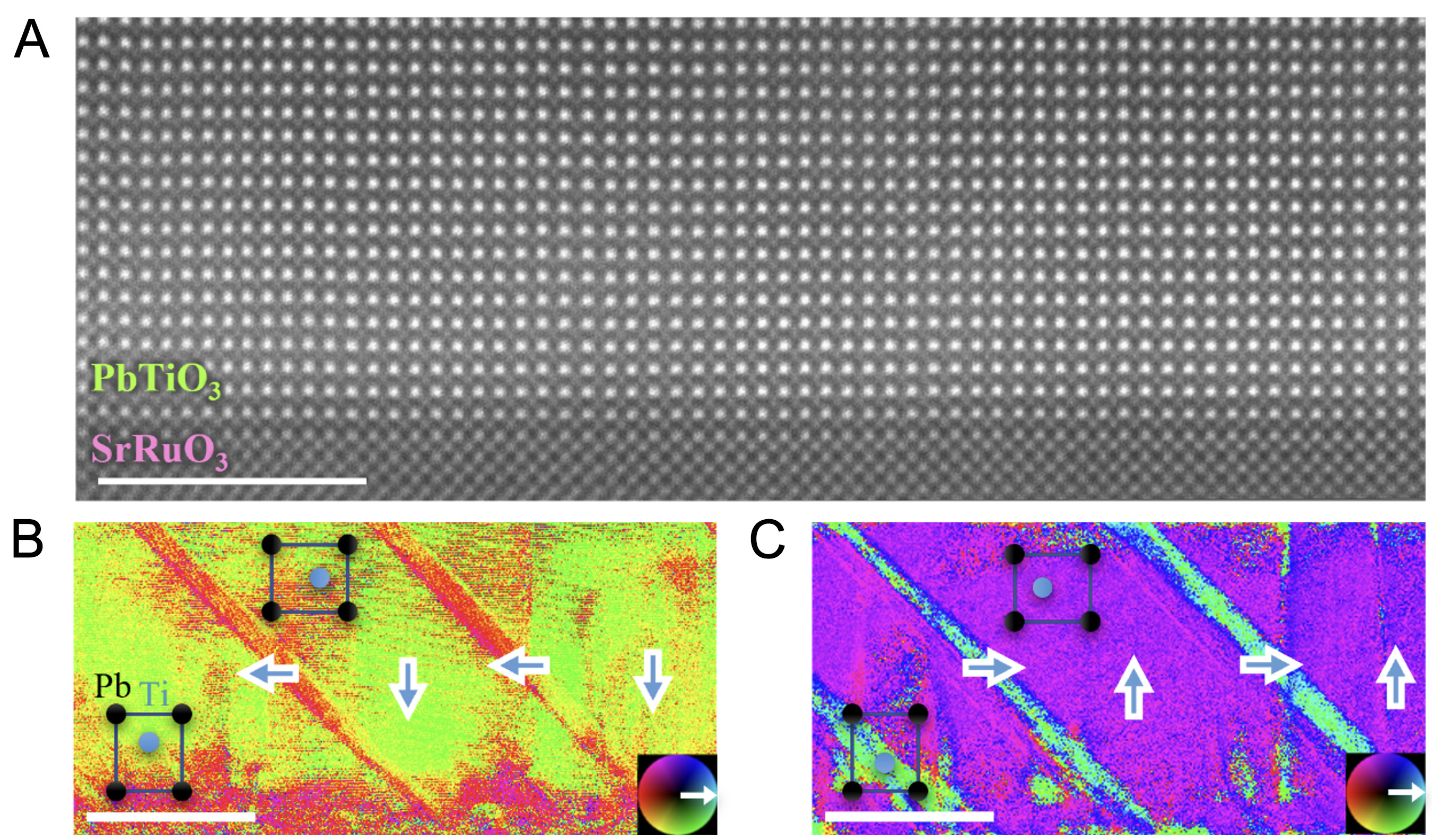
Figure 1. (A) HAADF-STEM image of the as-grown PTO/SRO films along the [100] zone axis. Reconstructed polarization vector maps in the 200 nm thick PTO films derived from DPC electric-field images acquired (B) before and (C) after poling. DPC analysis is restricted to PTO layer. Blue arrows indicate the polarization orientations of each domain corresponding to the schematic atomic structure. The white scale bar represents 5 nm in (A) and 100 nm in (B) and (C). HAADF: High-angle annular dark-field; PTO: PbTiO3; SRO: SrRuO3; DPC: differential phase contrast; STEM: scanning transmission electron microscopy.
Consistent with TEM results, the initial domain structure of thin line-shaped a-domains embedded in a crystallographic configuration between relatively large c-domains is also observed in the PFM amplitude mapping [Supplementary Figure 1C]. Moreover, bias-dependent PFM phase mapping under an applied voltage (Va) exceeding the coercive voltage (Vc) reveals that the initial electric polarization is oriented downward toward the SRO electrode [Supplementary Figure 1D]. Considering the clear c-domain switching observed when |Vc| < |Va|, the ferroelastic domain switching process was clarified through the following four steps: (1) identification of the initial domain structures; (2) application of a negative bias [Va < 0 or Va(-)] at the center of a large c-domain using a sweeping direct current (DC) bias combined with an alternating current (AC) voltage applied to the PFM tip [Supplementary Figure 1E]; (3) sweeping of a positive bias
When a voltage higher than the coercive voltage (|Vc| < |Va| = 7 V) was applied at position #1 [Figure 2A and B], reversal of the c-domain polarization was clearly observed, exhibiting a circular pattern at the edge of the reversed domain. An a-domain was newly formed during c-domain switching, even within the neighboring c-domain matrix [Figure 2B]. Once the a-domain was created, it remained even after the c-domain polarization was restored to its original downward state upon the application of Va = +7 V [Figure 2C], indicating irreversible c- to a-domain switching. The switched domain is further evident in the PFM phase mapping [Supplementary Figure 4A-C], displaying a circular contrast in the reversed region as well as a 180° switched phase signal. After the initial formation of the a-domain, no additional a-domains were generated under similar bias-application procedures intended to induce c- to a -domain switching within the reduced c-domain matrix (#2 and #3 in Figure 2C). Because the formation of an a-domain during c-domain switching has been attributed to strain-energy relaxation, the restriction on further a-domain formation within the same volume can also be understood in terms of limited strain relaxation[9,24,31,33].
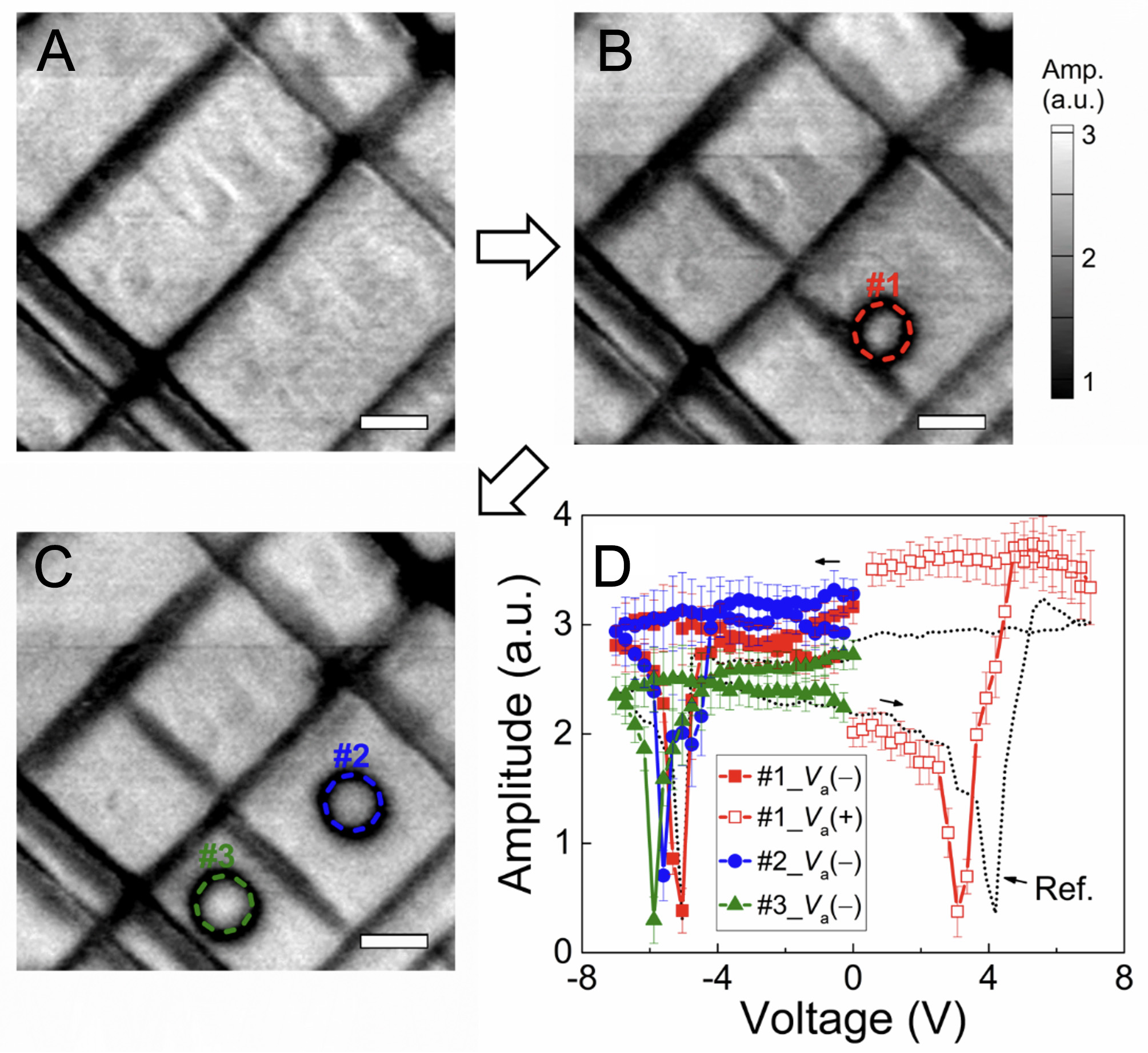
Figure 2. PFM amplitude images of (A) the initial state, (B) Va = -7 V at position #1, and (C) Va = -7 V at positions #2 and #3 following Va = +7 V at position #1. The white scale bar represents 200 nm; (D) Voltage-dependent PFM amplitude curves measured at positions #1 (red squares), #2 (blue circles), and #3 (green triangles) under negative [Va(-), closed symbols] and positive [Va(+), open symbols] bias. The conventional amplitude response near the tested c-domain (dotted black line) is shown for reference. Black arrows indicate the direction of the voltage sweeps. PFM: Piezoelectric force microscopy.
The PFM amplitude and phase loops under the condition |Vc| < |Va| are presented in Figure 2D and Supplementary Figure 4D, obtained throughout the domain switching procedure. The typical PFM amplitude signal (black dotted line in Figure 2D) proves clear c-domain switching at approximately 4~5 V, whereas the similar amplitude values at 0 V between the initial state and Va(-) yield a pronounced contrast at the edges of domains with different electric polarizations. The P-E hysteresis curves [Supplementary Figure 1B] also support clear polarization switching at Vc < Va. However, unlike the PFM results, the P-E loops exhibit a much lower coercive voltage (Vc ≈ 2 V), which can be attributed to the different measurement mechanisms and macroscopic contributions, such as charge transport, leakage current, interfacial effects, and experimental conditions.
A conventional PFM amplitude and phase loop was observed at position #1 under Va(-), showing a significant change at Vc. Given the lower Vc compared to the other cases where |Va| < |Vc|, and the absence of clear evidence for c- to a-domain switching at V < Vc, the localized reduction of the c-domain switching barrier causes it to closely merge with the c- to a-domain switching voltage in the PFM amplitude curve. This overlap makes a clear distinction between c-domain switching and a-domain formation difficult. In addition, once the a-domain is created, Vc for c-domain switching back to the initial state [Vc(+) = +3 V] is considerably lower than usual, probably due to the assistance of the a-domain in nucleating reversed c-domains[1]. Meanwhile, slightly increased Vc values were observed at positions #2 and #3 compared to #1, i.e., c-domain switching accompanied by a-domain formation (#1) occurred at Vc = -5.0 V, whereas switching without a-domain formation (#2 and #3) occurred at Vc = -5.5~-6.0 V. These results suggest a correlation between c-domain switching and a-domain formation, indicating that the strain energy released by a-domain creation[9,24,31,33] facilitates switching more readily than pure c-domain reversal.
To further investigate strain-related a-domain formation, a voltage lower than Vc (|Va| = 4 V < |Vc|) was applied at position #4 [Figure 3A and B] to restrict c-domain switching. A clear a-domain was created in the middle of the c-domain and persisted even after subsequent application of positive voltages (at position #4 and #5 in Figure 3C). This phenomenon is more evident in the PFM phase mapping results in Supplementary Figure 5, showing a clear contrast from the created a-domain without observable c-domain switching, unlike the case of |Vc| < |Va|. However, PFM amplitude measurements provide better insight into c- to a-domain switching, as the piezoelectric coefficient of a-domains (d24 = 56 pm/V)[36] is ~30% smaller than that of c-domains (d33 = 79 pm/V)[36]. This is also evident in the PFM amplitude mappings due to distinctly different PFM values at 0 V for c- and a-domains, represented by gray and black contrasts, respectively. In Figure 3D, an elliptical PFM amplitude loop (red dotted line) was observed in the c-domain region under Va < Vc due to the unswitched c-domain polarization, whereas a typical PFM amplitude loop (black dotted line) were observed under Vc < Va. At position #4, a pronounced drop in amplitude at
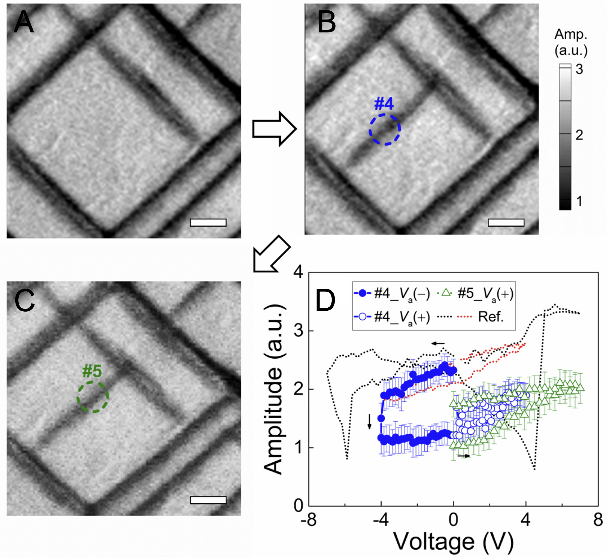
Figure 3. PFM amplitude images of (A) the initial state, (B) Va = -4 V at position #4, and (C) Va = +4 V at positions #4 following Va = +7 V at position #5. The white scale bar represents 200 nm; (D) Voltage-dependent PFM amplitude curves measured at positions #4 (blue circles), #5 (green triangles) under negative [Va(-), closed symbols] and positive [Va(+), open symbols] bias. The conventional amplitude response near the tested c-domain (dotted black and red lines) is shown for reference. Black arrows indicate the direction of the voltage sweeps. PFM: Piezoelectric force microscopy.
The created a-domain did not revert to c-domain even after applying Vc < Va = 7 V at the position #5 (green triangles in Figure 3D), instead exhibiting a larger elliptical loop. According to the previous research[30], the creation and annihilation of a-domains within a c-domain matrix depend on overcoming the energy barrier associated with the a/c domain boundary. However, the electrostatic and elastic energies induced by the applied bias, together with the a/c domain wall surface energy, are insufficient to fully explain the observed irreversible ferroelastic switching, as these mechanisms are generally limited to reversible processes. Recent studies[40-42] have demonstrated that misfit dislocations and point defects introduce local strain fields that alter the domain wall dynamics and create additional energy pathways for domain motion. They suggested that the role of local strain is not a passive obstacle that hinders switching, but rather it acts as a key design variable that actively programs the switching path and reversibility by locally reconfiguring the energy landscape. Therefore, for a comprehensive understanding of ferroelastic switching in PTO thin films, the effects of local strain induced by structural deformations (e.g., defects and dislocations) should also be taken into account.
Considering the domain switching shown in Figures 2 and 3, a-domain formation initiates from specific positions where the voltage is applied. This suggests that partially generated, transient a-domain fragments at the biased positions within the c-domain act as nucleation sites for c- to a-domain switching and subsequently propagate along crystallographic directions to regions without applied voltage. Consequently, the interconnected a-domains represent a more energetically stable state compared to isolated partial a-domains within the c-domain. This observation is consistent with the PFM mapping results, in which a-domains are predominantly interconnected [Supplementary Figure 1C] and remain stable even under conditions of Vc < Va (position #5 in Figure 3C). Conversely, this implies that if partial a-domains are generated under specific conditions, they have the potential to revert to c-domains upon application of bias voltage, enabling reversible c- to a-domain switching. To examine this possibility, the following procedure was performed: (1) obtaining the initial domain structures, (2) applying bipolar Va, which involves first applying Va(-) immediately followed by Va(+) at the center of a c-domain to determine whether partial a-domain structures were formed, and (3) moving to the partial a-domains and applying Va(+) to induce switching back from a-domain to c-domain.
In Figure 4A and B, a partial a-domain is formed without connection to other a-domains upon application of Va = 6 V at position #6. The newly formed a-domain exhibits a discrete line structure, with the switched-back c-domain observed at the tip bias position. The remaining fragments of a-domains were also reverted to c-domains upon additional application of Va(+) = +7 V, as shown in Figure 4C. To understand the piezo-response associated with reversible c- to a-domain switching, the bias-dependent PFM amplitude was plotted in Figure 4D, obtained during the DC sweeping process. A complete hysteresis loop is observed at position #6, with significant drops in amplitude at Vc→a = -4.2 V and recovered to the initial value at Va→c = +3.5V. This domain switching does not include c-- to c+-domain switching, as Vc(-) = -6.7 V, which is also evident in the PFM phase results in Supplementary Figure 6, showing no clear changes during c- to a-domain switching. Furthermore, application of Va(+) also does not switch the c-domain at Va = +6 V, even when it exceeds Vc(+) = +4.5 V, because the initial electric polarization of PTO is directed downward toward the SRO electrodes. Unlike the well-defined hysteresis observed in the PFM amplitude at position #6, the remaining fragments of a-domains (#7 and #8) exhibit gradual increases in amplitude during application of Va(+) = +7 V to switch back to c-domains. These changes in PFM amplitude may be associated with the unstable states of the remaining a-domains, which could also relate to the relatively high and low PFM amplitude values at Va = 0 V before and after bias application, respectively, compared to those observed at #6.
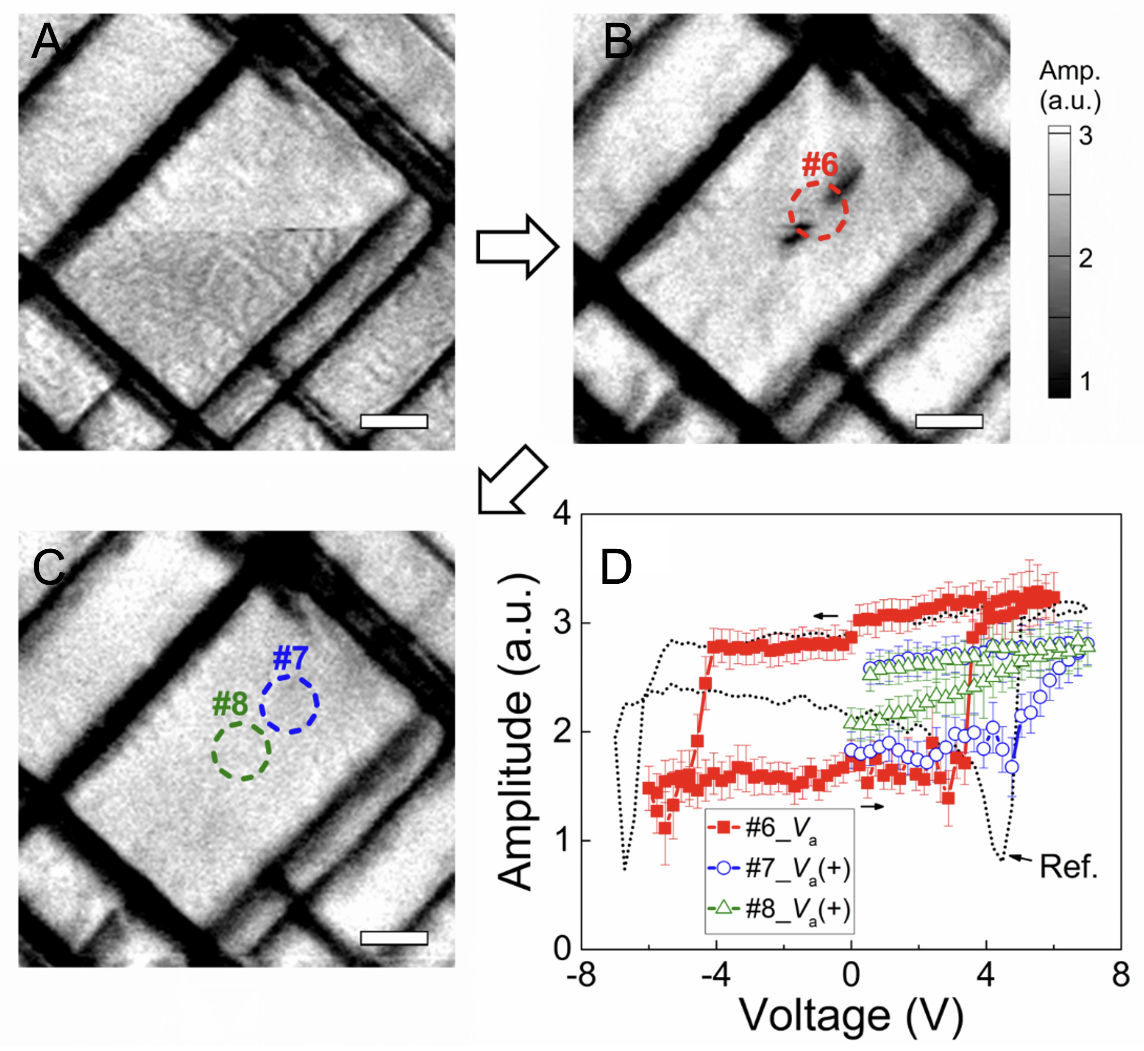
Figure 4. PFM amplitude images of (A) the initial state, (B) Va = -4V followed by + 4V at position #6, and (C) Va = +7 V at positions #7 and #8. The white scale bar represents 200 nm; (D) Voltage-dependent PFM amplitude curves measured at positions #6 (red squares), #7 (blue circles), and #8 (green triangles) under bipolar (Va, closed symbols) and positive [Va(+), open symbols] bias. The conventional amplitude response near the tested c-domain (dotted black lines) is shown for reference. Black arrows indicate the direction of the voltage sweeps. PFM: Piezoelectric force microscopy.
To understand the mechanisms underlying domain switching, a thermodynamic model was employed that considers the total free energy (ΔFtotal) consisting of voltage-induced electrostatic (
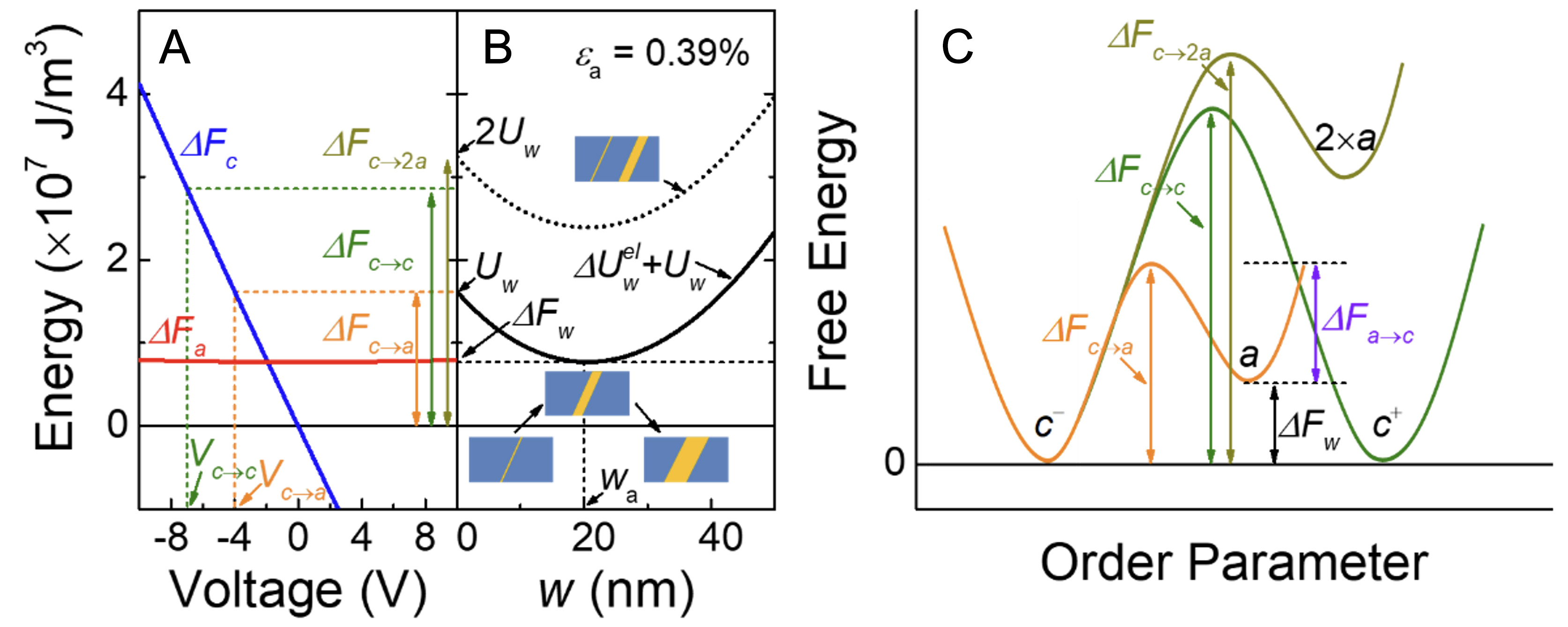
Figure 5. (A) Free energies of the pristine c-domain (ΔFc (V); black line) and newly formed a-domain (ΔFa (V) + ΔFw; red line) as a function of applied voltages. Coercive voltages for c- to a- (Vc→a) and c- to c- (Vc→c) domain switching and their corresponding free energies ΔFc→a (orange dashed line) and ΔFc→c (green dashed line) are indicated. Energy required for formation of a second a-domain (ΔFc→2a); brown arrow) is also shown; (B) Elastic energy (
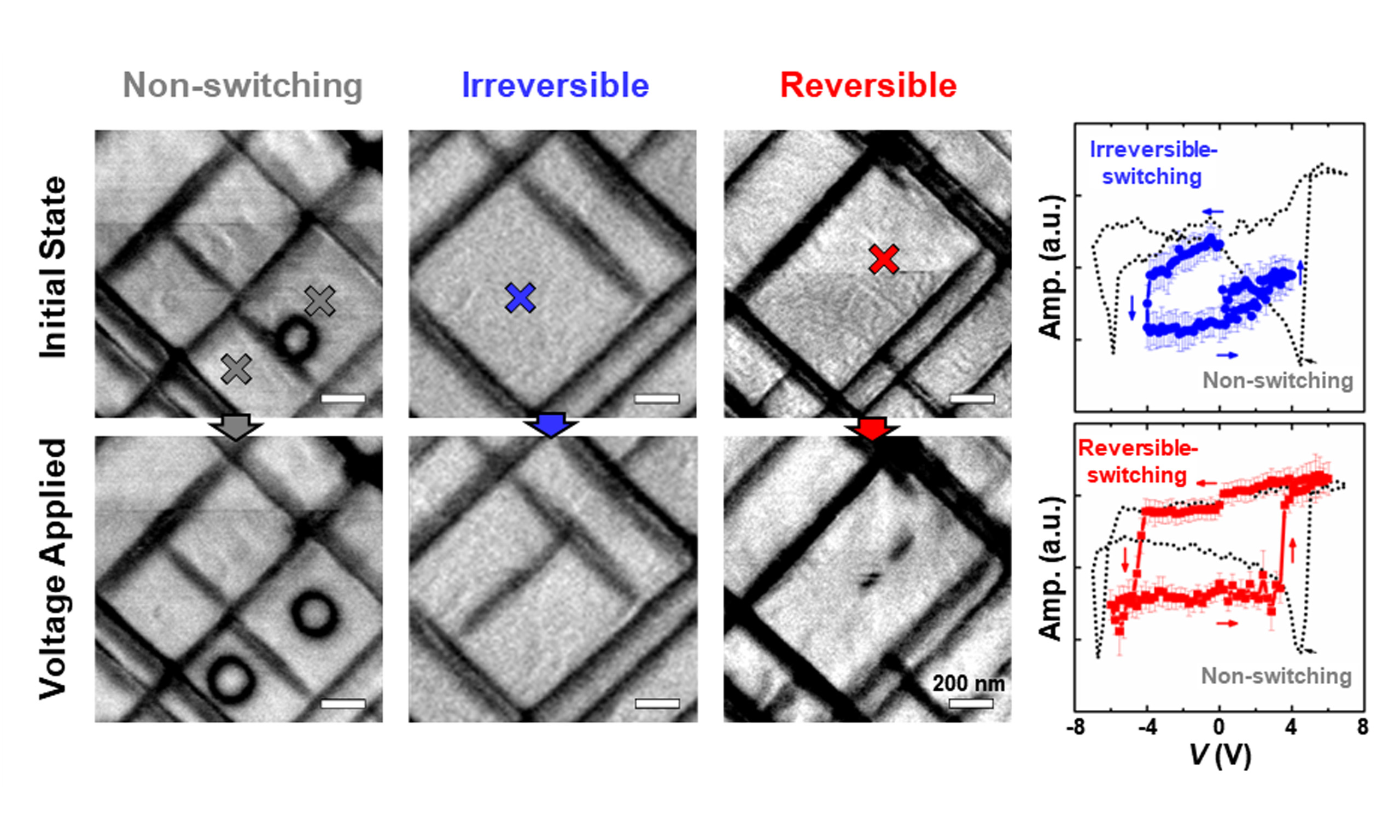
From the PFM results, three types of domain switching were identified, which are further evidenced by the formation of various a-domains after area bias application at VDC = -4 V [Supplementary Figure 7]: (i) non-switching, (ii) irreversible c- to a-domain switching, and (iii) reversible c- to a-domain switching. (i) Non-switching: The energy required to form an a-domain depends on the surface area of the a/c-domain wall [Figure 5B and C]. Therefore, creating a second a-domain within the same unit volume of the c-domain matrix requires twice the surface energy (ΔFc→2a = 2Uw). However, the voltage needed to form this second a-domain exceeds Vc→c ≈ +6 V, causing c-domain switching to occur before the second a-domain can form [Figure 2C]. In addition, as the number of a-domains increases, the total free energy of the system also rises, energetically limiting the number of a-domains that can form within a given c-domain volume.
(ii) Irreversible c- to a-domain switching: A new a-domain can be created in a pristine c-domain matrix by overcoming the a/c-domain wall energy Uw and releasing strain energy to reach ΔFw (εa) under |Va| < |Vc|. To achieve a- to c-domain switching, ΔFa (V) should become comparable to ΔFc (V), similar to the c- to a-domain switching mechanism [Figure 5C]. This requires applying a positive voltage to PTO so that the energy state of the c-domain matches that of the a-domain. However, in most cases excessive release of strain energy makes it impossible to reach ΔFc (V) without causing significant leakage currents or electrical breakdown. Our calculations indicate that a tip bias of +62 V would be required to switch an a-domain back to a c-domain, a level at which the thin film cannot be sustained due to excessive electric current. Therefore, enabling a- to c-domain switching without electrical damage requires modifying ΔFw (εa) by tuning εa.
(iii) Reversible c- to a-domain switching: In PTO structures, strain is typically relaxed by forming a-domains due to the large misfit between the in-plane lattice parameters of SRO (bSRO) and PTO (aPTO). If aPTO is locally increased by defects or dislocations, the formation of an a-domain within the c-domain matrix releases insufficient strain energy [Figure 6A and B], allowing the a-domain to switch back to the c-domain. To explain this ferroelastic domain switching using the thermodynamic model, the influence of local strain should be considered because both ΔFw (εa) and ΔFa→c depend on εa (inset of Figure 6B). Therefore, increasing εa lowers ΔFa→c, enabling ferroelastic switching from the a- to the c-domain at lower positive voltages.
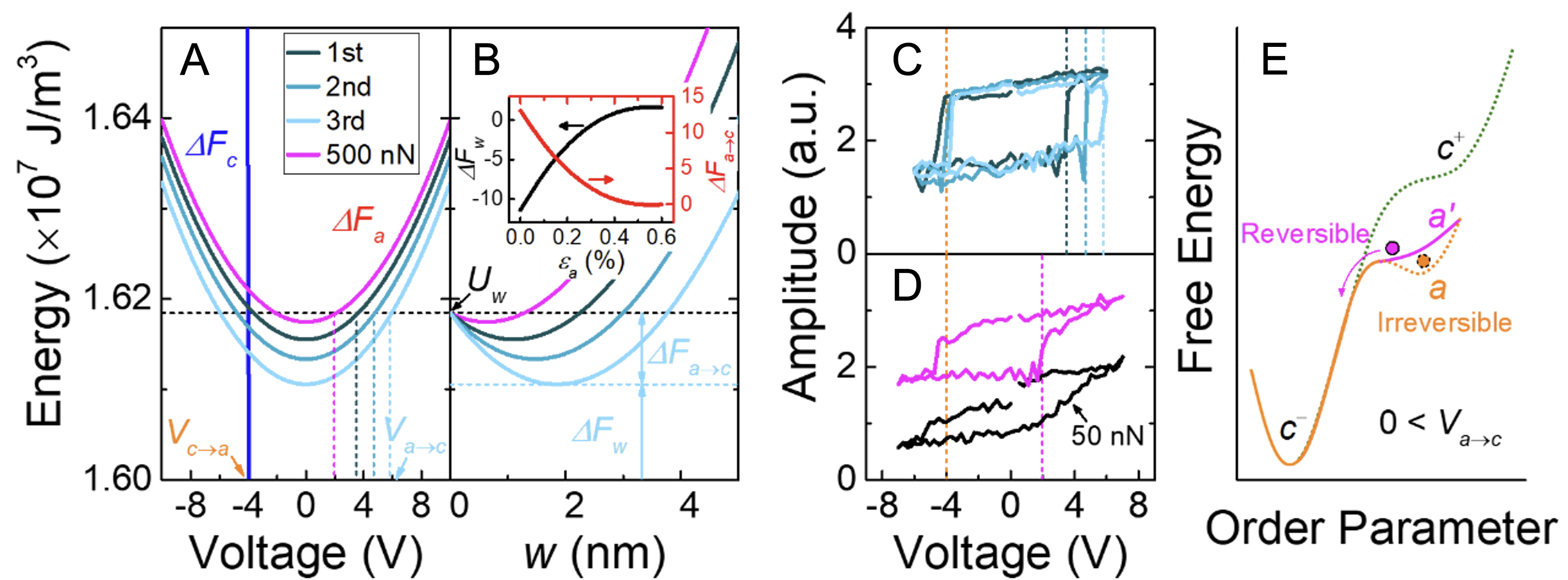
Figure 6. (A) Free energies as a function of applied voltages for newly formed a-domains [ΔFa (V)] during the 1st (dark cyan line), 2nd (medium cyan line), and 3rd (light cyan line) voltage sweeps, together with the tip contact force of 500 nN (magenta line). Corresponding coercive voltages for a- to c-domain switching (Va→c) required to overcome the surface energy (Uw, black dashed line) are indicated; (B) Elastic energy versus a-domain width for the voltage sweeps (same color code as in A). The elastic energy at wa (ΔFw), and the energy barrier for a- to c-domain switching (ΔFa→c) during the 3rd voltage sweep are marked as examples. The inset shows strain (εa) dependent ΔFw (black line, left y-axis) and ΔFa→c (red line, right y-axis). PFM amplitude as a function of voltage for (C) the three voltage sweeps (same color code as in A) and for (D) tip contact forces of 500 nN (magenta line) and 50 nN (black line). Corresponding Va→c for each voltage sweep and tip contact force are indicated and Vc→a (orange dashed line) is shown for comparison. (E) Schematic energy diagram for irreversible (a; orange) and reversible (a’; magenta) a-domains under 0 < Va→c, compared with the transition from c+ (green) to c-. PFM: Piezoelectric force microscopy.
Consistent with this context, we experimentally confirmed the presence of local strain within the PTO film. Because this strain originates from the lattice misfit between the PTO and SRO layers, it is naturally associated with substrate-induced mismatch as well as growth-related defects that accumulate during epitaxy. Dark-field TEM (DF-TEM) imaging clearly visualizes contrast variations arising from threading dislocations along the vertical direction and from strain fields localized near the interface [Supplementary Figure 8]. To obtain more quantitative evidence of the interfacial strain, we performed lattice-parameter analysis using atomic-scale HAADF-STEM [Supplementary Figure 9]. The extracted tetragonality map of PTO film reveals distinct in-plane lattice strain confined to the interfacial region, which is fully consistent with the expected strain distribution in this heterostructure and corroborates our theoretical calculations. Therefore, the phenomenological results can be interpreted within the thermodynamic model as a function of εa.
Because ferroelastic switching is accompanied by structural deformation, the influence of defects with high energy states diminishes as they relax toward normal lattice configurations. Consequently, as the number of ferroelastic switching cycles (n) increases, newly formed a-domains release progressively more free energy [Figure 6A-C]. In contrast, Vc→a remains unchanged regardless of n, as c- to a-domain switching depends on Uw rather than εa. This leads to the asymmetric PFM amplitude-voltage hysteresis loops, where Vc→a stays constant while Va→c increases with n, as shown for the nth loops in Figure 6C. To validate the εa-induced ferroelastic switching model, a tip contact force was applied to the a-domain at position #5 in Figure 2, where irreversible a- to c-domain switching was observed even at Va = 7 V (black line in Figure 6D). Increasing the tip contact force reduces both the tetragonality (α) and lattice misfit (Φ), thereby lowering the relaxation energy in a manner similar to that of structurally defect-induced εa. Although PFM amplitude mapping under 500 nN tip force was not feasible for direct visualization of the ferroelastic transition, the bias-dependent PFM amplitude curves clearly reveal a- to c-domain switching [Figure 6D]. The amplitude exhibits an abrupt increase at +2 V, maintains the value throughout the voltage sweep, and returns to its original value at -4 V. This behavior closely resembles the ferroelastic switching observed in Figure 6C, where Va→c varies with εa while Vc→a remains nearly constant during voltage cycling, with similar amplitude values observed during the a- to c-domain switching process. The retention and fatigue characteristics of the reversibly switched a-domains do not yet demonstrate the long-term stability required for practical applications. Repeated cycles of reversible c- to a-domain switching indicate that as n increases, Va→c also increases, causing the switching behavior to gradually become more irreversible [Figure 6C and E]. These limitations in stability strongly suggest a path for future device optimization through precise strain engineering, e.g., tuning strain, defect density, and film thickness.
The fundamental mechanism of reversible c- to a-domain switching under sub-coercive fields is driven by local strain inhomogeneity. This mechanism is not exclusive to the PTO/SRO heterostructures but reflects a general ferroelastic switching principle. It is applicable across a broad range of ferroelectric systems containing unconventional domain switching, in which ferroelastic transitions follow low-energy elastic pathways activated by local strain gradients or structural disorder, regardless of material composition. For instance, Pb(Zr,Ti)O3 films exhibit sub-coercive ferroelastic rotation at defect-rich or strain-perturbed regions[31]. Similarly, BiFeO3 shows dramatically enhanced mobility of its 71° and 109° ferroelastic boundaries where strain relaxation occurs[28]. Comparable trends emerge in compositionally graded ferroelectrics[33] and HfO2-based systems[43], reinforcing that the same strain-coupled mechanism governs accessible switching routes. Although the thermodynamic model presented here is specific to PTO, the governing physical terms (elastic energy, domain-wall energy, strain-dependent electrostatic contribution) are material-independent and establish a conceptual framework where local elastic inhomogeneity can be used to program domain switching across diverse ferroelastic materials.
CONCLUSIONS
In this study, we demonstrate that selective and reversible switching of a-domains can be achieved by exploiting intrinsic strain inhomogeneities under sub-coercive voltages. Localized structural perturbations associated with partially formed a-domains significantly reduce the elastic energy barriers and total free energy, thereby enabling reversible a- to c-domain transitions. By systematically comparing three distinct types of domain transitions (non-switching, irreversible switching, and reversible switching) we identified a strong correlation with variations in the local strain environment. That is, reversible switching occurs predominantly in strain-perturbed regions where metastable domain configurations are favored. Although mechanical loading experiments also altered the elastic energy landscape, they were less effective than intrinsic defects in sustaining reversible switching, highlighting the critical role of local structural inhomogeneity. While our findings establish the fundamental mechanism, the observed stability limitations emphasize that advanced strain engineering is the direct and most promising route to enhance the retention and cyclability for device applications. The ability to achieve sub-coercive switching is key for energy efficiency and scalability down to the nanoscale, offering excellent integration potential for reconfigurable logic gates and non-volatile memories. Our work establishes intrinsic strain control as a viable strategy for programmable ferroelastic switching and paves the way for designing reconfigurable ferroic devices through nanoscale elastic-field manipulation.
DECLARATIONS
Authors’ contributions
Experiment design and supervision: Sung, K. D.; Choi, S. Y.
Methodology: Sung, K. D.; Kim, G. Y.; Song, K.; Hong, S.
Data analysis: Sung, K. D.; Kim, M. S.; Jang, J.; Kim, G. Y.; Song, K.
Manuscript writing: Sung, K. D.; Kim, M. S.; Jang, J.
Manuscript review: Sung, K. D.; Kim, M. S.; Jang, J.; Kim, G. Y.; Song, K.; Hong, S.; Choi, S. Y.
All authors have read and agreed to the published version of the manuscript.
Availability of data and materials
The data that support the findings of this study are available from the corresponding author upon reasonable request.
AI and AI-assisted tools statement
During the preparation of this manuscript, the AI tools ChatGPT (OpenAI GPT-5, released 2025-08-07) and Gemini (Google Gemini 2.5 Flash, released 2025-06-17) were used solely for language editing. These tools did not influence the study design, data collection, analysis, interpretation, or the scientific content of the work. All authors take full responsibility for the accuracy, integrity, and final content of the manuscript.
Financial support and sponsorship
This work was supported by the Nano & Material Technology Development Program through the National Research Foundation of Korea (NRF) funded by Ministry of Science and ICT (RS-2024-00444182) and National R&D Program through the National Research Foundation of Korea (NRF) funded by Ministry of Science and ICT (RS-2023-00258227).
Conflicts of interest
All authors declared that there are no conflicts of interest.
Ethical approval and consent to participate
No applicable.
Consent for publication
No applicable.
Copyright
© The Author(s) 2026.
Supplementary Materials
REFERENCES
1. Gao, P.; Britson, J.; Jokisaari, J. R.; et al. Atomic-scale mechanisms of ferroelastic domain-wall-mediated ferroelectric switching. Nat. Commun. 2013, 4, 2791.
2. Nelson, C. T.; Gao, P.; Jokisaari, J. R.; et al. Domain dynamics during ferroelectric switching. Science 2011, 334, 968-71.
3. Lee, J. K.; Shin, G. Y.; Song, K.; et al. Direct observation of asymmetric domain wall motion in a ferroelectric capacitor. Acta. Mater. 2013, 61, 6765-77.
4. Baek, S. H.; Eom, C. B. Reliable polarization switching of BiFeO3. Philos. Transact. A. Math. Phys. Eng. Sci. 2012, 370, 4872-89.
5. Baek, S. H.; Jang, H. W.; Folkman, C. M.; et al. Ferroelastic switching for nanoscale non-volatile magnetoelectric devices. Nat. Mater. 2010, 9, 309-14.
6. Baek, S.; Choi, S.; Kim, T. L.; Jang, H. W. Domain engineering in BiFeO3 thin films. Curr. Appl. Phys. 2017, 17, 688-703.
7. Tang, Y. L.; Zhu, Y. L.; Wang, Y. J.; et al. Atomic-scale mapping of dipole frustration at 90° charged domain walls in ferroelectric PbTiO3 films. Sci. Rep. 2014, 4, 4115.
8. Zhang, Y.; Xie, L.; Kim, J.; et al. Discovery of a magnetic conductive interface in PbZr0.2Ti0.8O3/SrTiO3 heterostructures. Nat. Commun. 2018, 9, 685.
9. Gao, P.; Nelson, C. T.; Jokisaari, J. R.; et al. Revealing the role of defects in ferroelectric switching with atomic resolution. Nat. Commun. 2011, 2, 591.
10. McQuaid, R. G.; McGilly, L. J.; Sharma, P.; Gruverman, A.; Gregg, J. M. Mesoscale flux-closure domain formation in single-crystal BaTiO3. Nat. Commun. 2011, 2, 404.
11. Balke, N.; Choudhury, S.; Jesse, S.; et al. Deterministic control of ferroelastic switching in multiferroic materials. Nat. Nanotechnol. 2009, 4, 868-75.
12. Jang, J.; Choi, S. Reduced dimensional ferroelectric domains and their characterization techniques. Microstructures 2024, 4, 2024016.
13. Ganpule, C. S.; Roytburd, A. L.; Nagarajan, V.; et al. Polarization relaxation kinetics and 180° domain wall dynamics in ferroelectric thin films. Phys. Rev. B. 2001, 65, 014101.
14. Kim, T. H.; Baek, S. H.; Yang, S. M.; et al. Electric-field-controlled directional motion of ferroelectric domain walls in multiferroic BiFeO3 films. Appl. Phys. Lett. 2009, 95, 262902.
15. Kim, T. H.; Jeon, B. C.; Min, T.; et al. Continuous control of charge transport in Bi‐deficient BiFeO3 films through local ferroelectric switching. Adv. Funct. Mater. 2012, 22, 4962-8.
16. Nesterov, O.; Matzen, S.; Magen, C.; Vlooswijk, A. H. G.; Catalan, G.; Noheda, B. Thickness scaling of ferroelastic domains in PbTiO3 films on DyScO3. Appl. Phys. Lett. 2013, 103, 142901.
17. Venkatesan, S.; Vlooswijk, A.; Kooi, B. J.; et al. Monodomain strained ferroelectricPbTiO3 thin films: phase transition and critical thickness study. Phys. Rev. B. 2008, 78, 104112.
18. Highland, M. J.; Fister, T. T.; Fong, D. D.; et al. Equilibrium polarization of ultrathin PbTiO3 with surface compensation controlled by oxygen partial pressure. Phys. Rev. Lett. 2011, 107, 187602.
19. Kim, Y. K.; Kim, S. S.; Shin, H.; Baik, S. Thickness effect of ferroelectric domain switching in epitaxial PbTiO3 thin films on Pt(001)/MgO(001). Appl. Phys. Lett. 2004, 84, 5085-7.
20. Feigl, L.; Yudin, P.; Stolichnov, I.; et al. Controlled stripes of ultrafine ferroelectric domains. Nat. Commun. 2014, 5, 4677.
21. Sheng, G.; Zhang, J. X.; Li, Y. L.; et al. Domain stability of PbTiO3 thin films under anisotropic misfit strains: phase-field simulations. J. Appl. Phys. 2008, 104, 054105.
22. Mahjoub, R.; Anbusathaiah, V.; Alpay, S. P.; Nagarajan, V. Ferroelastic domains in bilayered ferroelectric thin films. J. Appl. Phys. 2008, 104, 124103.
23. Yuan, G.; Huang, H.; Li, C.; Liu, D.; Cheng, Z.; Wu, D. Ferroelastic‐Domain‐Assisted Mechanical Switching Of Ferroelectric Domains in Pb(Zr,Ti)O3 thin films. Adv. Elect. Mater. 2020, 6, 2000300.
24. Pompe, W.; Gong, X.; Suo, Z.; Speck, J. S. Elastic energy release due to domain formation in the strained epitaxy of ferroelectric and ferroelastic films. J. Appl. Phys. 1993, 74, 6012-9.
25. Ivry, Y.; Wang, N.; Chu, D.; Durkan, C. 90°domain dynamics and relaxation in thin ferroelectric/ferroelastic films. Phys. Rev. B. 2010, 81, 174118.
26. Vogel, A.; Sarott, M. F.; Campanini, M.; Trassin, M.; Rossell, M. D. Monitoring electrical biasing of Pb(Zr0.2Ti0.8)O3 ferroelectric thin films in situ by DPC-STEM imaging. Materials. 2021, 14, 4749.
27. Nagarajan, V.; Roytburd, A.; Stanishevsky, A.; et al. Dynamics of ferroelastic domains in ferroelectric thin films. Nat. Mater. 2003, 2, 43-7.
28. Zhang, Y.; Han, M. G.; Garlow, J. A.; et al. Deterministic ferroelastic domain switching using ferroelectric bilayers. Nano. Lett. 2019, 19, 5319-26.
29. Ivry, Y.; Chu, D.; Scott, J. F.; Salje, E. K.; Durkan, C. Unexpected controllable pair-structure in ferroelectric nanodomains. Nano. Lett. 2011, 11, 4619-25.
30. Chen, L.; Ouyang, J.; Ganpule, C. S.; Nagarajan, V.; Ramesh, R.; Roytburd, A. L. Formation of 90° elastic domains during local 180° switching in epitaxial ferroelectric thin films. Appl. Phys. Lett. 2004, 84, 254-6.
31. Khan, A. I.; Marti, X.; Serrao, C.; Ramesh, R.; Salahuddin, S. Voltage-controlled ferroelastic switching in Pb(Zr0.2Ti0.8)O3 thin films. Nano. Lett. 2015, 15, 2229-34.
32. Gao, P.; Britson, J.; Nelson, C. T.; et al. Ferroelastic domain switching dynamics under electrical and mechanical excitations. Nat. Commun. 2014, 5, 3801.
33. Agar, J. C.; Damodaran, A. R.; Okatan, M. B.; et al. Highly mobile ferroelastic domain walls in compositionally graded ferroelectric thin films. Nat. Mater. 2016, 15, 549-56.
34. Woo, J.; Hong, S.; Setter, N.; et al. Quantitative analysis of the bit size dependence on the pulse width and pulse voltage in ferroelectric memory devices using atomic force microscopy. J. Vac. Sci. Technol. B. 2001, 19, 818-24.
35. Roelofs, A.; Szot, K.; Waser, R. Domain switching and self- polarization in perovskite thin films. In Nanoscale Phenomena in Ferroelectric Thin Films; Springer US, 2004; pp 135-55.
36. Haun, M. J.; Furman, E.; Jang, S. J.; Cross, L. E. Thermodynamic theory of the lead zirconate-titanate solid solution system, part V: theoretical calculations. Ferroelectrics 1989, 99, 63-86.
37. Palneedi, H.; Yeo, H. G.; Hwang, G.; et al. A flexible, high-performance magnetoelectric heterostructure of (001) oriented Pb(Zr0.52Ti0.48)O3film grown on Ni foil. APL. Mater. 2017, 5, 096111.
38. Peräntie, J.; Stratulat, M. S.; Hannu, J.; Jantunen, H.; Tyunina, M. Enhancing polarization by electrode-controlled strain relaxation in PbTiO3 heterostructures. APL. Mater. 2016, 4, 016104.
39. Dorywalski, K.; Lemée, N.; Gharbi, M.; et al. VIS-UV-VUV optical functions of epitaxial ferroelectric PbTiO3/SrTiO3 thin films. Opt. Mater. 2025, 162, 116930.
40. Feng, Y. P.; Jiang, R. J.; Zhu, Y. L.; et al. Strain coupling of ferroelastic domains and misfit dislocations in [101]-oriented ferroelectric PbTiO3 films. RSC. Adv. 2022, 12, 20423-31.
41. Henning, X.; Alhada-lahbabi, K.; Deleruyelle, D.; et al. Oxygen vacancy effects on polarization switching of ferroelectricBi2FeCrO6 thin films. Phys. Rev. Mater. 2024, 8, 054416.
42. Bulanadi, R.; Cordero-Edwards, K.; Tückmantel, P.; et al. Interplay between point and extended defects and their effects on jerky domain-wall motion in ferroelectric thin films. Phys. Rev. Lett. 2024, 133, 106801.
Cite This Article
How to Cite
Download Citation
Export Citation File:
Type of Import
Tips on Downloading Citation
Citation Manager File Format
Type of Import
Direct Import: When the Direct Import option is selected (the default state), a dialogue box will give you the option to Save or Open the downloaded citation data. Choosing Open will either launch your citation manager or give you a choice of applications with which to use the metadata. The Save option saves the file locally for later use.
Indirect Import: When the Indirect Import option is selected, the metadata is displayed and may be copied and pasted as needed.
About This Article
Special Topic
Copyright

Data & Comments
Data
0


Comments
Comments must be written in English. Spam, offensive content, impersonation, and private information will not be permitted. If any comment is reported and identified as inappropriate content by OAE staff, the comment will be removed without notice. If you have any queries or need any help, please contact us at [email protected].