

Multiscale simulations of Ge–Sb–Se–Te phase-change alloys for photonic memory applications
 0
0 
Abstract
Phase-change materials (PCMs) are among the most promising candidates for next-generation non-volatile memory and neuromorphic computing technologies. However, their photonic applications are hindered by a trade-off between refractive index contrast and optical absorption losses. Artificial intelligence-assisted computational approaches are essential for fundamental understanding and device modeling of PCMs. In this work, we systematically investigate structural and optical properties of crystalline and amorphous Ge2Sb2SexTe5-x (x = 0 to 4) alloys using density functional theory (DFT), and then use the DFT-computed optical parameters for modeling and optimization of photonic computing devices via the finite-difference time-domain method. Among the investigated compositions, we identify a promising candidate, i.e., Ge2Sb2Se3Te2 for all-optical switching on a silicon-on-insulator (SOI) platform. Finally, we design a dual-disk PCM waveguide structure on SOI with an enhanced switching contrast and a low optical loss for scalable photonic neural network application.
Keywords
INTRODUCTION
Phase-change materials (PCMs) are one of the leading candidates for the development of non-volatile memory and neuromorphic in-memory computing devices[1-8]. The basic principle is to utilize the electrical or optical contrast between the amorphous and crystalline states of PCMs for information encoding. The flagship PCMs are the Ge–Sb–Te alloys (GST) along the pseudo-binary line between GeTe and Sb2Te3, which can enable rapid and reversible phase transition between the two solid states using electrical or optical pulses. The PCM-based electronic memory cards for both stand-alone and embedded applications are already commercially available in the memory market. By tuning the amorphous-to-crystalline ratio in a single memory cell, multilevel memory operations can be realized, and the whole array can be used for in-memory computing to process artificial intelligence (AI) tasks[9]. By integrating PCM with the silicon-on-insulator (SOI) waveguide devices, PCM can be effectively programmed in the all-optical mode for photonic memory and in-memory computing[10]. In comparison with PCM electronic devices, PCM photonic devices offer much wider bandwidth for data transfer and the wavelength division multiplexing (WDM) capability for highly parallelized data processing. Recently, AI-based methods[11-14] have started to play an active role in PCM research, including fingerprint classification[15,16], combinatorial experiments[17,18] and high-throughput simulations[19-22], implementation of machine-learned (ML) potentials for atomic simulations[23-32], and so on. The new memory and in-memory computing technologies are expected to further boost the development of advanced AI methods[33-35].
Computer simulations play a central role in PCM research. Density functional theory (DFT) and DFT-based ab initio molecular dynamics (AIMD) simulations have been extensively applied to understand the fundamental properties of both crystalline and amorphous PCMs[36-42]. The comparison between experiments and ab initio simulations has promoted the development of new PCMs for embedded and universal memory applications[43,44]. Towards device-scale modeling, there are two major routes. One route is to construct effective ML interatomic potentials[45] via DFT-based structural database and then carry out ML-driven molecular dynamics (MLMD) directly at the device scale (containing millions of atoms)[46-49]. The other route is to transfer the DFT-calculated physical parameters to the coarse-grained device simulation packages and perform simulations in specific device setups[50]. In the former route, all the dynamical atomic structures are transferred, and in the latter route, only critical parameters are transferred for device-scale modeling. Both simulation schemes can provide guidance for further device experiments. These simulation protocols are summarized in Figure 1.
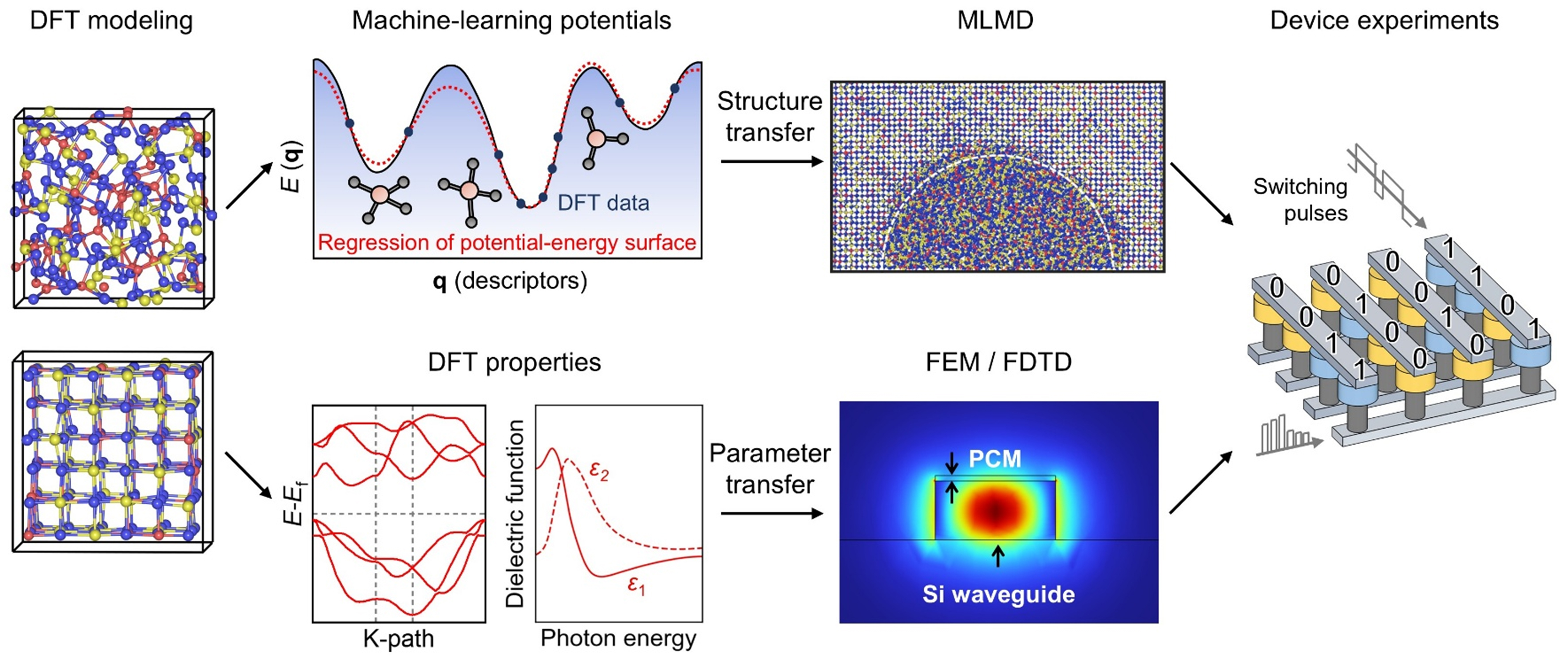
Figure 1. Integrated computational and experimental workflow for material and device modeling. The MLMD figure panel was adapted with permission from Ref.[46], Nature Portfolio. MLMD: Machine-learned-driven molecular dynamics.
The Ge2Sb2Te5 (GST) alloy was extensively applied in waveguide memory devices. Upon phase transition, GST undergoes a major change in bonding character, i.e., metavalent bonding (MVB)[51,52] with highly aligned p orbitals for the crystalline phase and covalent bonding with more localized bonding features for the amorphous phase, and such change results in a large optical window for encoding information. However, the size of the waveguide device array is limited to a few tens of devices because of relatively high optical loss in the crystalline GST state[53]. Se substitution can largely reduce the optical loss, and an optimal composition of Ge2Sb2Se4Te1 (GSST) was achieved for low-loss photonic applications[54-56]. Yet, the extinction coefficient of GSST is too low to enable heating via light absorption. An effective hybrid mode with electrical-switching and optical-read was developed for GSST waveguide devices[57] but at a cost of higher programming power due to electrical programming.
Too much Se content tends to cause GSST to form an orthorhombic crystalline phase of Ge2Sb2Se5, where the degree of MVB is reduced due to the misalignment of p orbitals in the outer shell of the unit cell. The X-ray diffraction (XRD) measurements under different annealing temperatures[54] showed that Ge2Sb2Se3Te2 and Se-poorer Ge–Sb–Se–Te alloys followed a similar trend as GST, namely, forming firstly a cubic rock-salt phase upon crystallization and then gradually transforming to a layered trigonal phase at high annealing temperatures[58]. Regarding theoretical modeling of Ge–Sb–Se–Te alloys, only ordered layered crystalline models were considered[54]. However, this is not sufficient to account for the high degree of atomic disorder in rock-salt GST and possibly also in Se-poorer Ge–Sb–Se–Te alloys. Note that the rock-salt phase and the amorphous phase are the two technologically relevant phases for GST devices, and both of them contain a high degree of atomic disorder. The crystalline structure of rock-salt GST contains a fully occupied Te sublattice, and the second sublattice is shared by Ge (40%), Sb (40%) and atomic vacancies (20%)[59-61].
Here, we report a multiscale simulation work of Ge–Sb–Se–Te alloys for all-optical waveguide applications. We adopt the parameter transfer simulation protocol. The workflow includes the following steps: (a) atomic model construction via DFT/AIMD; (b) electronic structure and optical calculations via DFT; (c) building finite-difference time-domain (FDTD) models with DFT-calculated and experimentally measured refractive indices; and (d) performing FDTD waveguide device simulations and optimization of the device structure. We calculate the electronic and optical properties of four Ge–Sb–Se–Te alloys in orthorhombic, rock-salt and amorphous phases. Then we focus on the Ge2Sb2Se3Te2 alloy for all-optical waveguide device simulations, because this composition shows a reduced extinction coefficient, but can still yield a sizable contrast in light absorption as compared to the amorphous phase. Finally, we propose a disk-shaped (DS) fully-etched waveguide device structure for photonic synaptic applications using Ge2Sb2Se3Te2, and we predict such a structure to have a favorable trade-off between optical contrast and optical loss.
MATERIALS AND METHODS
Using DFT and AIMD, we constructed orthorhombic (o-), rock-salt (rs-) and amorphous (a-) models of Ge2Sb2Se1Te4 (GSS1T4), Ge2Sb2Se2Te3 (GSS2T3), Ge2Sb2Se3Te2 (GSS3T2) and Ge2Sb2Se4Te1 (GSS4T1) alloys. The o-phase represents the crystalline phase of Ge2Sb2Se5 (GSS)[54], and each model contains 72 atoms in an orthorhombic box. The rs-phase represents the metastable phase of GST upon rapid crystallization[59-61], and each model contains 324 atoms and 36 vacant sites in an orthorhombic box. The atomic structures of amorphous Ge–Sb–Se–Te models were taken from our previous work[62], which were generated following a standard melt-quenched procedure using CP2K[63]. Each amorphous model contains 360 atoms in a cubic box. All the atomic structures were further relaxed with the VASP code[64]. The projector augmented wave (PAW) method[65] and the Perdew-Burke-Ernzerhof (PBE) functional[66] were used with an energy cutoff of 500 eV. For the small o-phase models, a k-point mesh of 1 × 6 × 1 was used, and for the large rs-phase and a-phase models, only the gamma point was used to sample the Brillouin zone. For optical calculations, the number of bands (Nband) was set to twice the default value, where the default is defined as the sum of the number of valence electrons (Nelectron) and the number of atoms (Natom), i.e., Nband = Nelectron + Natom. The k-point density along each lattice direction was doubled (for the large models) or tripled (for the small o-phase models) for all models, for better convergence of the calculated optical properties.
We employed the FDTD method[67] to model a silicon waveguide with a width of 450 nm on a 2-μm-thick SiO2 substrate, and analyzed the optical responses of the waveguide decorated with PCMs. The frequency-domain profile monitors were placed surrounding the PCM waveguide to monitor transmission, reflection, and scattering characteristics, while additional cross-sectional profile monitors were positioned to analyze the electric-field distribution and PCM absorption. The excitation source was set as the fundamental TE mode, propagating along the positive x-direction, with the wavelength range covering the telecommunication bands (1,500-1,600 nm). Perfectly matched layer (PML) boundary conditions were applied along all three (x, y, z) axes. Due to the thin PCM layer on the waveguide, a locally refined mesh with 1-nm resolution in the z-direction was implemented for the PCM region, while the entire FDTD simulation domain adopted an auto non-uniform mesh configuration. Specifically, the transmission monitor was positioned at x = 3 µm, while the reflection monitor was symmetrically placed at x = -3 µm. The scattering monitors were located 2 µm away from the PCM waveguide device in y and z directions. The excitation source was positioned at x = -1.8 µm. The FDTD simulation domain spanned over 8 µm × 5 µm × 4.5 µm along the x-, y-, and z-axis, respectively, with PML boundary conditions applied for all boundaries.
RESULTS AND DISCUSSION
The phase transition between the rs-phase and a-phase of GST is exploited for practical applications, and the rs-phase is typically obtained via rapid crystallization after short laser or electrical pulses of nanosecond level[68,69]. The programming time to obtain the o-phase of GSS is much slower at the microsecond level[54,70]. For the intermediate compositions between GST and GSS studied in this work, i.e., Ge2Sb2SexTe5-x (x = 1 to 4) alloys, the crystalline phases formed during rapid device programming remain unclear. Therefore, both the o-phase and rs-phase were considered, as shown in Figure 2A and B. The o-phase consists of island-like structural blocks[54], where 9 atomic layers stack in sequence of X–Sb–X–Ge–X–Ge–X–Sb–X (X referring to the anion-like atoms Te/Se), resembling the Koo stacking of hexagonal GST[71]. Atoms within the blocks show distorted octahedral motifs with 6-fold coordination, but for atoms at the edge of blocks, the structural gap between blocks leads to weakening or breakage of p orbital alignment and reduction of coordination number to 3 (in the two terminal X layers) or 5 (in other layers). The rs-phase is composed of two face-centered cubic sublattices, where one sublattice is randomly occupied by Te/Se atoms and the other by Ge/Sb atoms or vacancies. Large models containing more than 300 atoms are built to account for this compositional disorder. In this phase, all the cation-like atoms (Ge and Sb) are in an octahedral configuration, where p orbitals are well aligned. Regarding the o-phase, the structural symmetry is reduced, as non-octahedral bonds are present, inducing misalignment of p orbitals. Figure 2C shows a-phase models of Ge–Sb–Se–Te alloys. Each model was generated through an independent melt-quenched simulation. The structural features are similar to those of a-GST, with defective octahedra taking a dominating role except for a minor fraction (25%-32%) of tetrahedral Ge motifs[62]. With the increase of Se content, there are more shorter bonds Ge–Se (~2.5 Å) and Sb–Se (~2.6 Å) compared with Ge–Te (~2.7 Å) and Sb–Te (~2.9 Å) in the amorphous models. More detailed structural analyses of amorphous Ge–Sb–Se–Te models can be found in Ref.[62]. For all these three phases, the increasing Se content results in reduction in box size, and thereby increase of atomic densities, from 0.0315 to 0.0341 Å-3 for the o-phase, from 0.0317 to 0.035 Å-3 for the rs-phase, and from 0.0287 to 0.03 Å-3 for the a-phase. All the structure files can be found in the CAID Repository (see the data availability note).
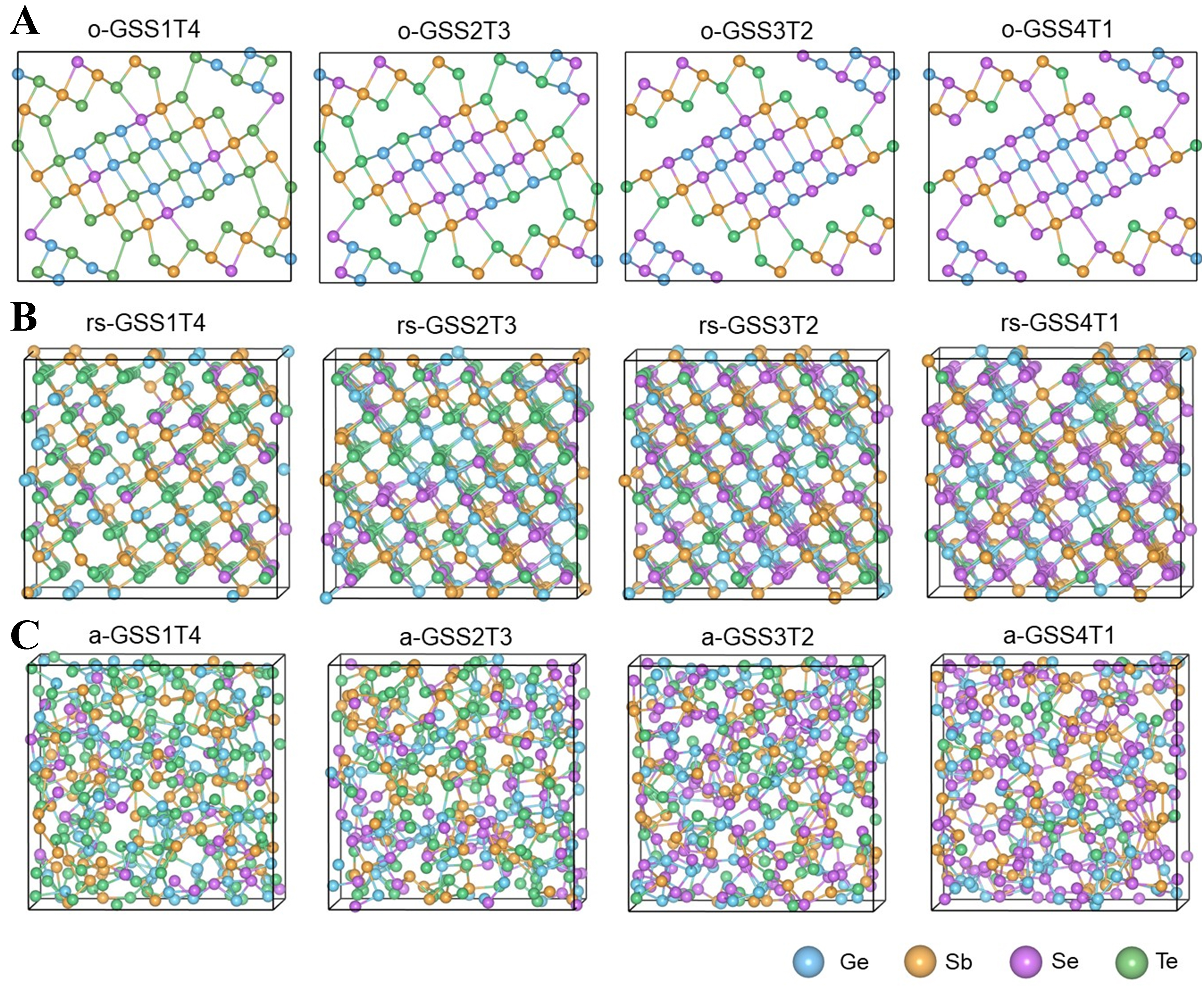
Figure 2. The DFT-optimized atomic structures of (A) orthorhombic, (B) cubic rock-salt and (C) amorphous phase for the four Ge–Sb–Se–Te compositions. The Ge, Sb, Se and Te atoms are rendered with blue, gold, purple and green spheres, respectively. DFT: Density functional theory.
The calculated density of states (DOS) curves are presented in Figure 3A, where all the phases exhibit semiconducting characteristics. With the increase of Se concentration, band gap is widened in all three phases, from 0.53 to 0.77 eV in the o-phase, from 0.29 to 0.40 eV in the rs-phase, and from 0.42 to 0.73 eV in the a-phase. This is attributed to enlarged charge transfer and strengthened atomic distortion induced by Se substitution. The o-phase shows larger band gap values than those of the rs-phase, which is associated with the lower coordination number and stronger atomic distortions and orbital hybridizations. Since the electronic band gap represents the energy threshold required for inter-band photon excitations, larger band gap values would help suppress optical absorption in the spectrum with low photon energy and long wavelength, e.g., the infrared spectrum. Note that the band gap sizes here are underestimated due to the inherent limitation of DFT calculations with PBE functional and more accurate results can be obtained with hybrid functional calculations[72]. However, our rs- and a-phase Ge–Sb–Se–Te models contain over 300 atoms per simulation box and exhibit high degrees of atomic disorder, making hybrid functional calculations difficult to converge. Nevertheless, this trend of increased band gap size upon selenium substitution for both amorphous and crystalline Ge–Sb–Se–Te is qualitatively correct, which is consistent with experimental data[73]. In Ref.[73], the optical band gap values measured experimentally are 0.77 and
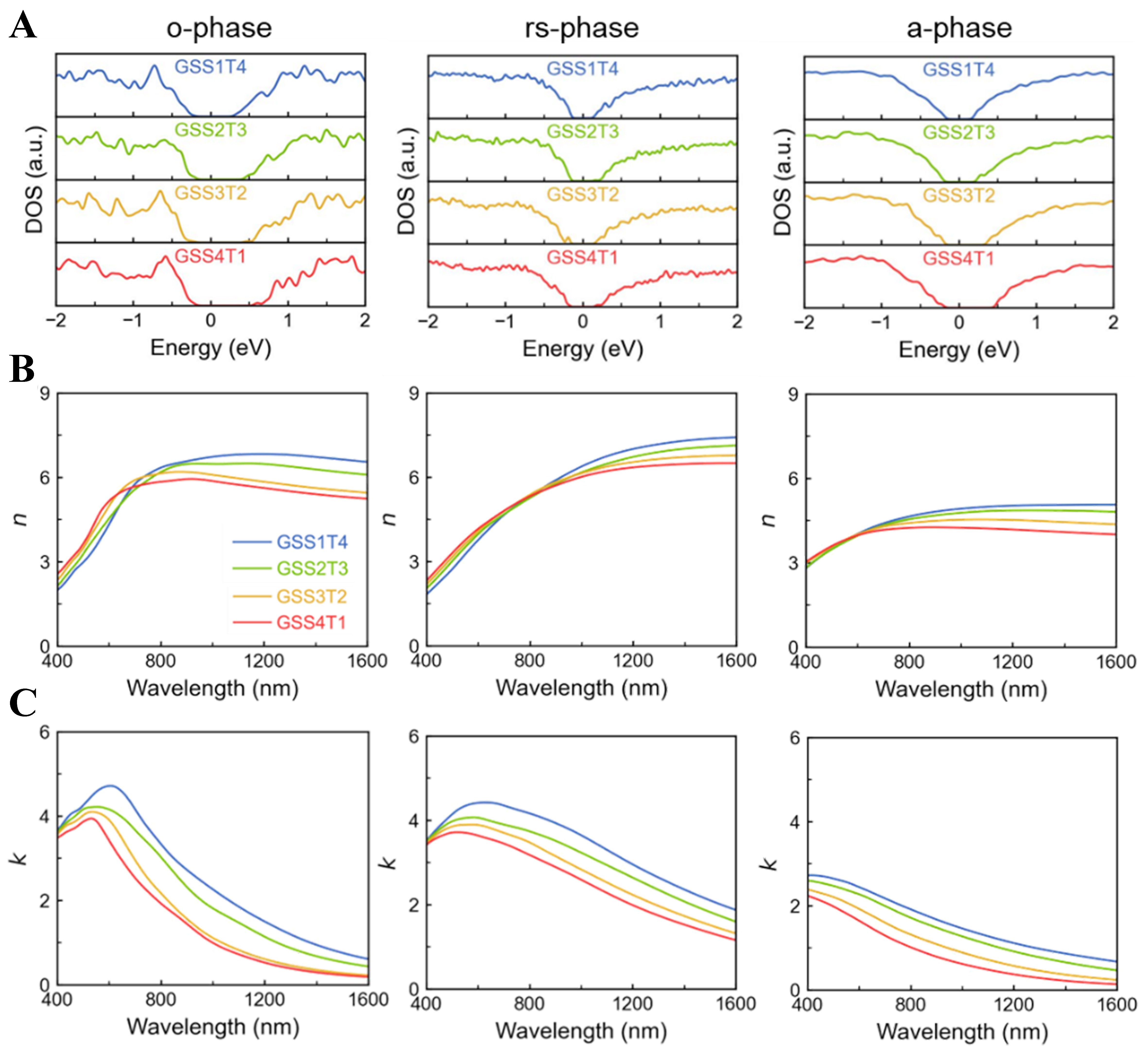
Figure 3. The DFT-calculated (A) DOS, (B) refractive index n and (C) extinction coefficient k of the o-, rs- and a-phase of the four Ge–Sb–Se–Te alloys. DFT: Density functional theory; DOS: density of states.
We performed DFT calculations of the real and imaginary parts of the dielectric functions (ε1 and ε2, respectively) with the independent-particle approximation[74-77] and derived the refractive index (n) and extinction coefficient (k) using
As shown in Figure 3B, n increases at shorter wavelengths and decreases at longer wavelengths with the increasing Se concentration for both o- and rs-phases, with the cross-over appearing in 600-800 nm and at ~800 nm, respectively. In the a-phase, n shows a systematic decrease across the spectrum range of
Next, we carried out photonic waveguide device modeling simulations through the FDTD method[67] using the DFT-calculated optical refractive indices. Figure 4A is a schematic of the simulation model, which is a 150-nm shallow-etched (SE) SOI waveguide covered with PCM and indium tin oxide (ITO) thin films. Thickness and width of the silicon waveguide are 0.22 and 0.45 μm, respectively. Thickness and length of PCM are defined as hPCM = 10 nm and dPCM = 1 μm, respectively. Thickness and length of ITO are 10 nm and 1 μm, respectively. Reflection (R), transmission (T), scattering (S) can be defined as below: R = Pref/Pinput, T = Ptrans/Pinput, S = Psca/Pinput, where Pref, Ptrans, Psca, and Pinput represent the reflected, transmitted, scattered, and input light power, respectively. The calculated refractive indices of the GST and Ge2Sb2SexTe5-x (x = 0 to 4) in the rs-phase and o-phase were imported into our FDTD model, leading to the two sets of transmittance spectra in Figure 4B and C. By increasing the Se substitution concentration, i.e., Ge2Sb2SexTe5-x (x = 0 to 4), we observed overall increase of transmittance values due to reduced loss by light absorption. For the rs-phase PCM, crystalline state shows a more pronounced decrease in transmittance than that of the orthorhombic phase due to stronger light absorption given its smaller band gap. We also simulated transmission spectra of waveguides with the a-phase Ge2Sb2SexTe5-x (x = 0 to 4) as shown in Figure 4D.
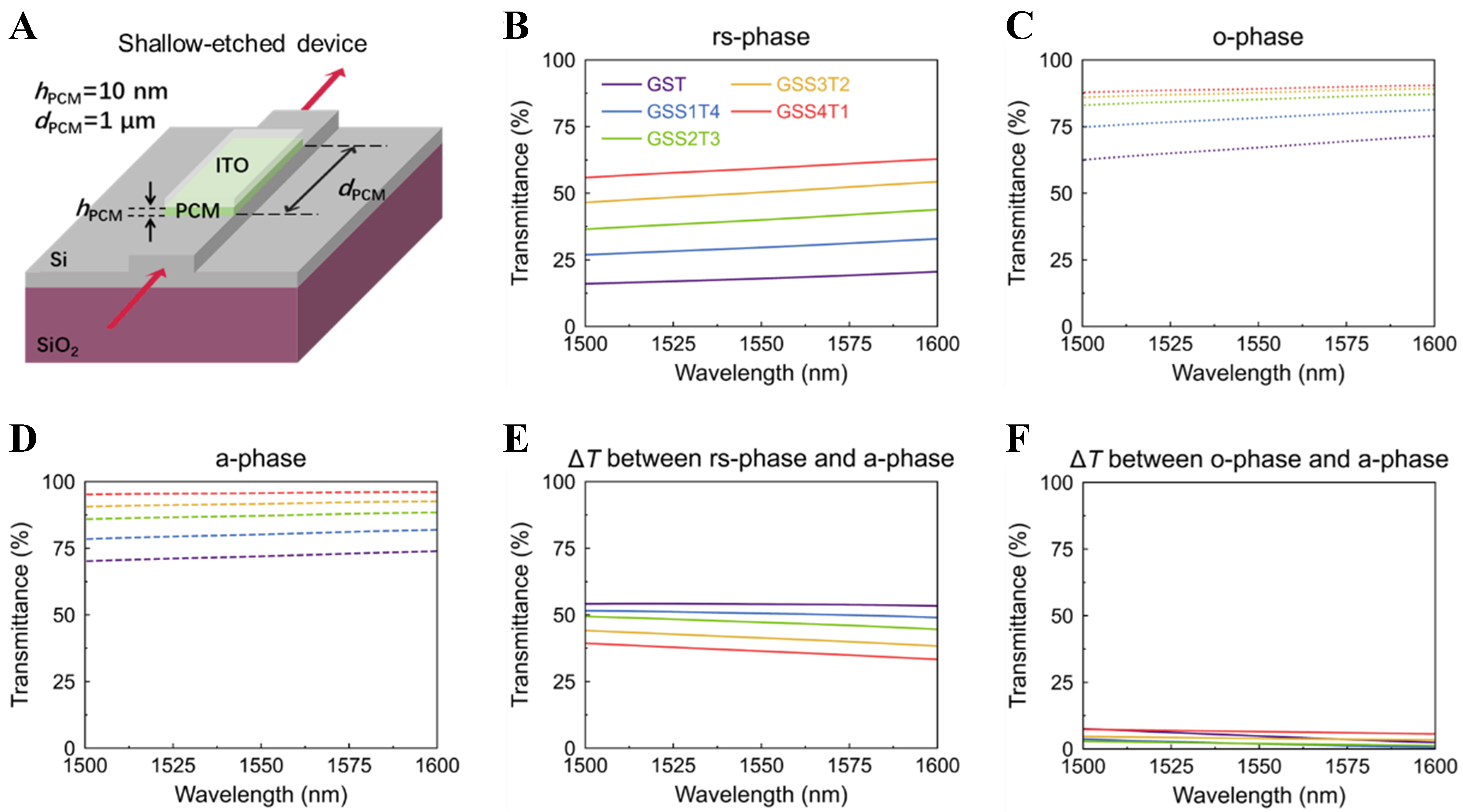
Figure 4. (A) A schematic of the PCM-decorated photonic waveguide. The PCM thickness hPCM and PCM length dPCM being 10 nm and
Figure 4E and F show the transmittance contrast (ΔT) of waveguides between the rs- (o-) phase and a-phase vs. substitution amount of Se. It shows a notable optical contrast (ΔT = 30%-55%) of the SOI waveguides between the rs-phase and a-phase, however, much smaller optical contrasts are observed (ΔT < 10%) between the o-phase and a-phase. Experimental results show that GST rapidly crystallizes into the rs-phase[59-61] upon laser or electrical pulsing. For Ge2Sb2SexTe5-x (x ≤ 3), a large Δk (> 1) was observed across the 1,500-1,600 nm wavelength band, but the Δk < ~0.4 was much reduced for GSS4T1 and GSS[54]. These optical behaviors can be attributed to the fact that the crystalline state of Ge2Sb2SexTe5-x (x ≤ 3) still adopts the rs-phase, but the other two compositions tend to take the o-phase. In terms of all-optical switching, GSS3T2 in the rs-phase is a more promising candidate than GSS4T1 of the o-phase due to a more pronounced signal contrast (ΔT). More importantly, the reduced but still non-negligible k of a- and rs-phases of GSS3T2 could enable efficient coupling with laser pulses to heat the material.
We performed FDTD simulations of SE devices using experimentally measured (n, k) and DFT-calculated ones. As shown in Figure 5A, the simulated transmission contrast between crystalline and amorphous phases GSS3T2 (red solid and red dashed lines) is comparable with that between the DFT-calculated rs-phase and a-phase (black solid and black dashed lines). However, the transmittance of o-phase GSS3T2 (black dotted line) is closer to that of a-phase GSS3T2. Based on the XRD pattern and optical measurements, the GSS3T2 should form rs-phase upon crystallization at low annealing temperatures[54]. Overall, the simulated transmission spectra based on the DFT-calculated refractive indices of GSS3T2 yield slightly higher optical losses, because the PBE functional underestimates the size of the band gap, leading to higher probabilities of inter-band transition. Using DFT-calculated and experimentally measured (n, k) values, the obtained device transmittance values at 1,550 nm are 50.37% and 57.68% for rock-salt GSS3T2, and 91.43% and 97.35% for amorphous GSS3T2. The errors are 12.70% and 6.08%, respectively. If hybrid functional DFT calculations can be performed, the error is expected to be reduced due to the increase of band gap value. Figure 5B displays the electric-field distributions of the three crystalline states as marked in Figure 5A, where light propagating through the waveguide is partially absorbed by the GSS3T2 thin film. The o-phase is highly transmissive, and is not feasible to serve as the OFF state.

Figure 5. (A) Transmission spectra of the SE waveguides at the telecommunication wavelength bands (1,500-1,600 nm) from FDTD simulations imported with DFT-simulated and experimentally measured refractive index data; (B) The simulated electric-field distributions of the GSS3T2 SE waveguides at 1,550 nm, as marked in (A). SE: Shallow-etched; FDTD: finite-difference time-domain; DFT: density functional theory; GSS3T2: Ge2Sb2Se3Te2.
To mimic neural networks, a waveguide crossbar array architecture was demonstrated based on the building blocks of waveguide memory cells[78-80]. Figure 6A shows the architecture of a crossbar array, in which a directional coupler is used to equally split light from row to column waveguides. PCM and ITO capping layers are deposited on the waveguide bend as to store the synaptic weight and modulate light transmission, simultaneously. The training of the photonic neural networks is based on refreshing matrix weights using phase transition of GST cells, while readout of matrix-vector multiplication results can be performed by measuring the light transmission at output ports. This neural network architecture provides inherent merits, including large scalability, broadband operation, parallel computing, and complementary metal-oxide-semiconductor (CMOS)-compatible fabrication. We calculated the transmission spectrum of the SE waveguide device decorated with GST, and obtained transmittance values of 93.7% and 25.4% for the a-phase and rs-phase GST at a wavelength of 1,550 nm, respectively. While this configuration demonstrates high signal contrast, the substantial optical loss of the crystalline phase limits upscaling of photonic neural networks.

Figure 6. (A) PCM-based photonic neural networks; (B) Sketch of GSS3T2-based FE device; (C) Sketch of GSS3T2-based DS device. The thickness hPCM, diameter DPCM and the gap between two neighboring PCM disks denoted as 14, 450 and 50 nm, respectively; The transmission spectra of c- and a-GSS3T2 integrated on (D) the FE waveguide device and (E) the DS waveguide device; (F) Reflection and scattering spectra of the two waveguide devices using crystalline GSS3T2. PCM: Phase-change material; GSS3T2: Ge2Sb2Se3Te2; FE: full-etched; DS: disk-shaped.
In principle, higher optical contrast could allow for the implementation of more transmittance levels for neuromorphic computing. Therefore, we also studied other waveguide structures to gradually extend the optical window. The etching depth is known to affect the transmittance of the waveguide devices. As shown in Figure 6B, we investigated the performance of GSS3T2 using a full-etched (FE) waveguide device with an etch depth of 220 nm. The red arrows in Figure 6B represent the full etching process of the silicon device layer. Moreover, we also simulated the GSS3T2 thin film in a DS pattern [Figure 6C], which consists of dual nano-disks positioned atop a single-mode silicon strip waveguide. This proposed design could enlarge the signal contrast by light scattering through the localized resonant effect[81], instead of light absorption.
Figure 6D shows simulated spectra of the FE devices using experimentally measured (n, k) of rs-phase and a-phase GSS3T2. Compared with the SE waveguide, the on-off switching contrast of the GSS3T2 is enhanced from 39.7% to 46.2% at a wavelength of 1,550 nm by using the FE waveguide. Regarding the DS device, the total volume of programmable PCM was set equivalent to that of a PCM thin-film in the FE device. Figure 6E shows a stronger switching contrast with transmittance values of the amorphous and crystalline GSS3T2 being 96.5% and 45.7% at 1,550 nm, respectively. Overall, the DS device showed an enhanced contrast of 50.8% at a wavelength of 1,550 nm as compared to the standard SE device. Figure 6F shows the simulated reflected power and scattered power of the FE and DS devices via FDTD. The nano-disk configuration supports low-order localized resonances, enabling enhanced scattering effects. Notably, most of the scattered light radiated into the substrate and free space. With localized resonant effect, the proposed DS design achieved balanced contrast window and low optical loss simultaneously.
CONCLUSIONS
In summary, this study provides multiscale simulations of the structural and optical properties of Ge–Sb–Se–Te alloys, identifying optimal compositions with significant refractive index contrast for all-optical non-volatile photonic switching and neuromorphic photonic computing applications. Based on the DFT-computed refractive indices, we simulated the transmission spectra of PCM-cladded SOI waveguides vs. the Ge–Sb–Se–Te composition. The FDTD simulations using various device structures highlight the potential of GSS3T2 for photonic synaptic applications with a favorable trade-off between optical contrast and propagation loss. These multiscale simulations provide atomic-scale understanding of the optical properties of GST with selenium substitution, and should serve as a stimulus for further experimental investigations of GSS3T2 for all-optical phase-change applications.
DECLARATIONS
Acknowledgments
We acknowledge the HPC platform of Xi’an Jiaotong University and the Computing Center in Xi’an for providing computational resources. The authors acknowledge XJTU for hosting their work at CAID. The International Joint Laboratory for Micro/Nano Manufacturing and Measurement Technologies of XJTU is acknowledged.
Authors’ contributions
Conceptualization: Zhang, W.; Zhang, H.; Zhou, W.
Multiscale calculations: Li, H.; Zhang, H.
Analysis of results: Ma, W.; Gao, Y.
Manuscript writing: Zhang, W.; Zhou, W.
Data discussion and analysis, and approval of the final version: Li, H.; Zhang, H.; Ma, W.; Gao, Y.; Zhou, W.; Zhang, W.
Availability of data and materials
The data that support the findings of this study are openly available in the CAID Repository at https://caid.xjtu.edu.cn/info/1003/2061.htm, reference number 2061.
Financial support and sponsorship
The authors acknowledge the support by the National Key Research and Development Program of China (No. 2023YFB4404500) and the National Natural Science Foundation of China (No. 62374131 and No. 62405242).
Conflicts of interest
All authors declared that there are no conflicts of interest.
Ethical approval and consent to participate
Not applicable.
Consent for publication
Not applicable.
Copyright
© The Author(s) 2026.
REFERENCES
1. Wuttig, M.; Yamada, N. Phase-change materials for rewriteable data storage. Nat. Mater. 2007, 6, 824-32.
2. Sebastian, A.; Le Gallo, M.; Khaddam-Aljameh, R.; Eleftheriou, E. Memory devices and applications for in-memory computing. Nat. Nanotechnol. 2020, 15, 529-44.
3. Lanza, M.; Pazos, S.; Aguirre, F.; et al. The growing memristor industry. Nature 2025, 640, 613-22.
4. Kim, H. J.; Julian, M.; Williams, C.; et al. Versatile spaceborne photonics with chalcogenide phase-change materials. NPJ. Microgravity. 2024, 10, 20.
5. Liu, B.; Li, K.; Zhou, J.; Sun, Z. Reversible crystalline-crystalline transitions in chalcogenide phase-change materials. Adv. Funct. Mater. 2024, 34, 2407239.
6. Li, X. D.; Chen, N. K.; Wang, B. Q.; et al. Resistive memory devices at the thinnest limit: progress and challenges. Adv. Mater. 2024, 36, e2307951.
7. Wang, Z.; Wu, H.; Burr, G. W.; et al. Resistive switching materials for information processing. Nat. Rev. Mater. 2020, 5, 173-95.
8. Wuttig, M.; Bhaskaran, H.; Taubner, T. Phase-change materials for non-volatile photonic applications. Nature. Photon. 2017, 11, 465-76.
9. Sebastian, A.; Le Gallo, M.; Burr, G. W.; Kim, S.; Brightsky, M.; Eleftheriou, E. Tutorial: Brain-inspired computing using phase-change memory devices. J. Appl. Phys. 2018, 124, 111101.
10. Youngblood, N.; Ríos Ocampo, C. A.; Pernice, W. H. P.; Bhaskaran, H. Integrated optical memristors. Nat. Photon. 2023, 17, 561-72.
11. Zeni, C.; Pinsler, R.; Zügner, D.; et al. A generative model for inorganic materials design. Nature 2025, 639, 624-32.
12. Merchant, A.; Batzner, S.; Schoenholz, S. S.; Aykol, M.; Cheon, G.; Cubuk, E. D. Scaling deep learning for materials discovery. Nature 2023, 624, 80-5.
13. Yuan, J.; Li, Z.; Yang, Y.; et al. Applications of machine learning method in high-performance materials design: a review. J. Mater. Inf. 2024, 4, 14.
14. Xu, D.; Zhang, Q.; Huo, X.; Wang, Y.; Yang, M. Advances in data-assisted high-throughput computations for material design. MGE. Advances. 2023, 1, e11.
15. Xu, M.; Xu, M.; Miao, X. Deep machine learning unravels the structural origin of mid-gap states in chalcogenide glass for high-density memory integration. InfoMat 2022, 4, e12315.
16. Schön, C. F.; van Bergerem, S.; Mattes, C.; et al. Classification of properties and their relation to chemical bonding: essential steps toward the inverse design of functional materials. Sci. Adv. 2022, 8, eade0828.
17. Kusne, A. G.; Yu, H.; Wu, C.; et al. On-the-fly closed-loop materials discovery via Bayesian active learning. Nat. Commun. 2020, 11, 5966.
18. Yuan, H.; Lu, J.; Zhuang, G.; Wang, H.; Hui, J. High-throughput screening of superlattice-like Ge-Sb-M (M = Sn, Se) thin films for multi-level phase change photonics materials. Microstructures 2025, 5, 2025053.
19. Liu, Y.; Li, X.; Zheng, H.; et al. High-throughput screening for phase-change memory materials. Adv. Funct. Mater. 2021, 31, 2009803.
20. Sun, S.; Wang, X.; Jiang, Y.; et al. High-throughput screening to identify two-dimensional layered phase-change chalcogenides for embedded memory applications. npj. Comput. Mater. 2024, 10, 1387.
21. Clima, S.; Matsubayashi, D.; Ravsher, T.; et al. In silico screening for As/Se-free ovonic threshold switching materials. npj. Comput. Mater. 2023, 9, 1043.
22. Abou El Kheir, O.; Bernasconi, M. High-throughput calculations on the decomposition reactions of off-stoichiometry GeSbTe alloys for embedded memories. Nanomaterials 2021, 11, 2382.
23. Sosso, G. C.; Miceli, G.; Caravati, S.; Behler, J.; Bernasconi, M. Neural network interatomic potential for the phase change material GeTe. Phys. Rev. B. 2012, 85, 174103.
24. Wang, G.; Sun, Y.; Zhou, J.; Sun, Z. PotentialMind: graph convolutional machine learning potential for Sb–Te binary compounds of multiple stoichiometries. J. Phys. Chem. C. 2023, 127, 24724-33.
25. Mocanu, F. C.; Konstantinou, K.; Lee, T. H.; et al. Modeling the phase-change memory material, Ge2Sb2Te5, with a machine-learned interatomic potential. J. Phys. Chem. B. 2018, 122, 8998-9006.
26. Sosso, G. C.; Miceli, G.; Caravati, S.; Giberti, F.; Behler, J.; Bernasconi, M. Fast crystallization of the phase change compound GeTe by large-scale molecular dynamics simulations. J. Phys. Chem. Lett. 2013, 4, 4241-6.
27. Dragoni, D.; Behler, J.; Bernasconi, M. Mechanism of amorphous phase stabilization in ultrathin films of monoatomic phase change material. Nanoscale 2021, 13, 16146-55.
28. Bosoni, E.; Campi, D.; Donadio, D.; Sosso, G. C.; Behler, J.; Bernasconi, M. Atomistic simulations of thermal conductivity in GeTe nanowires. J. Phys. D. Appl. Phys. 2020, 53, 054001.
29. Abou El Kheir, O.; Bonati, L.; Parrinello, M.; Bernasconi, M. Unraveling the crystallization kinetics of the Ge2Sb2Te5 phase change compound with a machine-learned interatomic potential. npj. Comput. Mater. 2024, 10, 1217.
30. Mo, P.; Zhang, Y.; Zhao, Z.; et al. High-speed and low-power molecular dynamics processing unit (MDPU) with ab initio accuracy. npj. Comput. Mater. 2024, 10, 1422.
31. Chen, Y.; Campi, D.; Bernasconi, M.; Mazzarello, R. Atomistic study of the configurational entropy and the fragility of supercooled liquid GeTe. Adv. Funct. Mater. 2024, 34, 2314264.
32. Yu, W.; Zhang, Z.; Wan, X.; et al. High-accuracy machine-learned interatomic potentials for the phase change material Ge3Sb6Te5. Chem. Mater. 2023, 35, 6651-8.
33. Ortner, T.; Petschenig, H.; Vasilopoulos, A.; et al. Rapid learning with phase-change memory-based in-memory computing through learning-to-learn. Nat. Commun. 2025, 16, 1243.
34. Li, H.; Xu, Y.; Duan, W. Ab initio artificial intelligence: future research of Materials Genome Initiative. MGE. Advances. 2023, 1, e16.
35. Syed, G. S.; Le Gallo, M.; Sebastian, A. Phase-change memory for in-memory computing. Chem. Rev. 2025, 125, 5163-94.
36. Sun, Z.; Zhou, J.; Ahuja, R. Structure of phase change materials for data storage. Phys. Rev. Lett. 2006, 96, 055507.
37. Wuttig, M.; Lüsebrink, D.; Wamwangi, D.; Wełnic, W.; Gillessen, M.; Dronskowski, R. The role of vacancies and local distortions in the design of new phase-change materials. Nat. Mater. 2007, 6, 122-8.
38. Caravati, S.; Bernasconi, M.; Kühne, T. D.; Krack, M.; Parrinello, M. Coexistence of tetrahedral- and octahedral-like sites in amorphous phase change materials. Appl. Phys. Lett. 2007, 91, 171906.
39. Akola, J.; Jones, R. O. Structural phase transitions on the nanoscale: the crucial pattern in the phase-change materials Ge2Sb2Te5 and GeTe. Phys. Rev. B. 2007, 76, 235201.
40. Wełnic, W.; Botti, S.; Reining, L.; Wuttig, M. Origin of the optical contrast in phase-change materials. Phys. Rev. Lett. 2007, 98, 236403.
41. Gan, Y.; Zhou, J.; Sun, Z. Prediction of the atomic structure and thermoelectric performance for semiconducting Ge1Sb6Te10 from DFT calculations. J. Mater. Inf. 2021, 1, 2.
42. Hempelmann, J.; Müller, P. C.; Ertural, C.; Dronskowski, R. The orbital origins of chemical bonding in Ge-Sb-Te phase-change materials. Angew. Chem. Int. Ed. Engl. 2022, 61, e202115778.
43. Song, Z.; Cai, D.; Cheng, Y.; et al. 12-state multi-level cell storage implemented in a 128 Mb phase change memory chip. Nanoscale 2021, 13, 10455-61.
44. Redaelli, A.; Petroni, E.; Annunziata, R. Material and process engineering challenges in Ge-rich GST for embedded PCM. Mater. Sci. Semicond. Process. 2022, 137, 106184.
45. Deringer, V. L.; Caro, M. A.; Csányi, G. Machine learning interatomic potentials as emerging tools for materials science. Adv. Mater. 2019, 31, e1902765.
46. Zhou, Y.; Zhang, W.; Ma, E.; Deringer, V. L. Device-scale atomistic modelling of phase-change memory materials. Nat. Electron. 2023, 6, 746-54.
47. Abou El Kheir, O.; Bernasconi, M. Million-atom simulation of the set process in phase change memories at the real device scale. Adv. Elect. Mater. 2025, e2500110.
48. Dunton, O. R.; Arbaugh, T.; Starr, F. W. Computationally efficient machine-learned model for GST phase change materials via direct and indirect learning. J. Chem. Phys. 2025, 162, 034501.
49. Wang, G.; Wang, C.; Zhang, X.; Li, Z.; Zhou, J.; Sun, Z. Machine learning interatomic potential: bridge the gap between small-scale models and realistic device-scale simulations. iScience 2024, 27, 109673.
50. Wang, X.; Zhou, W.; Zhang, H.; et al. Multiscale simulations of growth-dominated Sb2Te phase-change material for non-volatile photonic applications. npj. Comput. Mater. 2023, 9, 1098.
51. Wuttig, M.; Deringer, V. L.; Gonze, X.; Bichara, C.; Raty, J. Y. Incipient metals: functional materials with a unique bonding mechanism. Adv. Mater. 2018, 30, e1803777.
52. Raty, J. Y.; Schumacher, M.; Golub, P.; Deringer, V. L.; Gatti, C.; Wuttig, M. A quantum-mechanical map for bonding and properties in solids. Adv. Mater. 2019, 31, e1806280.
53. Zhang, Q.; Zhang, Y.; Li, J.; Soref, R.; Gu, T.; Hu, J. Broadband nonvolatile photonic switching based on optical phase change materials: beyond the classical figure-of-merit. Opt. Lett. 2018, 43, 94-7.
54. Zhang, Y.; Chou, J. B.; Li, J.; et al. Broadband transparent optical phase change materials for high-performance nonvolatile photonics. Nat. Commun. 2019, 10, 4279.
55. Zhang, Y.; Zhang, Q.; Ríos, C.; et al. Transient tap couplers for wafer-level photonic testing based on optical phase change materials. ACS. Photonics. 2021, 8, 1903-8.
56. Zhang, Y.; Fowler, C.; Liang, J.; et al. Electrically reconfigurable non-volatile metasurface using low-loss optical phase-change material. Nat. Nanotechnol. 2021, 16, 661-6.
57. Wei, M.; Xu, K.; Tang, B.; et al. Monolithic back-end-of-line integration of phase change materials into foundry-manufactured silicon photonics. Nat. Commun. 2024, 15, 2786.
58. Siegrist, T.; Jost, P.; Volker, H.; et al. Disorder-induced localization in crystalline phase-change materials. Nat. Mater. 2011, 10, 202-8.
59. Yamada, N.; Matsunaga, T. Structure of laser-crystallized Ge2Sb2+xTe5 sputtered thin films for use in optical memory. J. Appl. Phys. 2000, 88, 7020-8.
60. Park, J.; Park, G.; Baik, H.; Lee, J.; Jeong, H.; Kim, K. Phase-change behavior of stoichiometric Ge2Sb2Te5 in phase-change random access memory. J. Electrochem. Soc. 2007, 154, H139.
61. Zhang, B.; Zhang, W.; Shen, Z.; et al. Element-resolved atomic structure imaging of rocksalt Ge2Sb2Te5 phase-change material. Appl. Phys. Lett. 2016, 108, 191902.
62. Zhang, H.; Wang, X.; Zhang, W. First-principles investigation of amorphous Ge-Sb-Se-Te optical phase-change materials. Opt. Mater. Express. 2022, 12, 2497.
63. Hutter, J.; Iannuzzi, M.; Schiffmann, F.; Vandevondele, J. cp2k: atomistic simulations of condensed matter systems. WIREs. Comput. Mol. Sci. 2014, 4, 15-25.
64. Kresse, G. Ab initio molecular dynamics for liquid metals. J. Non. Cryst. Solids. 1995, 192-3, 222-9.
65. Kresse, G.; Joubert, D. From ultrasoft pseudopotentials to the projector augmented-wave method. Phys. Rev. B. 1999, 59, 1758-75.
66. Perdew, J. P.; Burke, K.; Ernzerhof, M. Generalized gradient approximation made simple. Phys. Rev. Lett. 1996, 77, 3865-8.
67. IncAnsys. Lumerical FDTD solutions. https://www.ansys.com/products/optics/fdtd. (accessed 13 Aug 2025).
68. Hase, M.; Fons, P.; Mitrofanov, K.; Kolobov, A. V.; Tominaga, J. Femtosecond structural transformation of phase-change materials far from equilibrium monitored by coherent phonons. Nat. Commun. 2015, 6, 8367.
69. Wu, D.; Yang, X.; Wang, N.; et al. Resonant multilevel optical switching with phase change material GST. Nanophotonics 2022, 11, 3437-46.
70. Meng, J.; Gui, Y.; Nouri, B. M.; et al. Electrical programmable multilevel nonvolatile photonic random-access memory. Light. Sci. Appl. 2023, 12, 189.
71. Kooi, B. J.; De, Hosson. J. T. M. Electron diffraction and high-resolution transmission electron microscopy of the high temperature crystal structures of GexSb2Te3+x (x = 1,2,3) phase change material. J. Appl. Phys. 2002, 92, 3584-90.
72. Heyd, J.; Scuseria, G. E.; Ernzerhof, M. Hybrid functionals based on a screened Coulomb potential. J. Chem. Phys. 2003, 118, 8207-15.
73. Koch, C.; Hansen, A.; Dankwort, T.; et al. Enhanced temperature stability and exceptionally high electrical contrast of selenium substituted Ge2Sb2Te5 phase change materials. RSC. Adv. 2017, 7, 17164-72.
74. Caravati, S.; Bernasconi, M.; Parrinello, M. First principles study of the optical contrast in phase change materials. J. Phys. Condens. Matter. 2010, 22, 315801.
75. Wełnic, W.; Wuttig, M.; Botti, S.; Reining, L. Local atomic order and optical properties in amorphous and laser-crystallized GeTe. C. R. Phys. 2009, 10, 514-27.
76. Xu, M.; Gu, R.; Qiao, C.; et al. Unraveling the structural and bonding nature of antimony sesquichalcogenide glass for electronic and photonic applications. J. Mater. Chem. C. 2021, 9, 8057-65.
77. Huang, B.; Robertson, J. Bonding origin of optical contrast in phase-change memory materials. Phys. Rev. B. 2010, 81, 081204.
78. Feldmann, J.; Youngblood, N.; Karpov, M.; et al. Parallel convolutional processing using an integrated photonic tensor core. Nature 2021, 589, 52-8.
79. Feldmann, J.; Youngblood, N.; Wright, C. D.; Bhaskaran, H.; Pernice, W. H. P. All-optical spiking neurosynaptic networks with self-learning capabilities. Nature 2019, 569, 208-14.
80. Shastri, B. J.; Tait, A. N.; Ferreira de Lima, T.; et al. Photonics for artificial intelligence and neuromorphic computing. Nat. Photonics. 2021, 15, 102-14.
Cite This Article
How to Cite
Download Citation
Export Citation File:
Type of Import
Tips on Downloading Citation
Citation Manager File Format
Type of Import
Direct Import: When the Direct Import option is selected (the default state), a dialogue box will give you the option to Save or Open the downloaded citation data. Choosing Open will either launch your citation manager or give you a choice of applications with which to use the metadata. The Save option saves the file locally for later use.
Indirect Import: When the Indirect Import option is selected, the metadata is displayed and may be copied and pasted as needed.
About This Article
Special Topic
Copyright

Data & Comments
Data
0


Comments
Comments must be written in English. Spam, offensive content, impersonation, and private information will not be permitted. If any comment is reported and identified as inappropriate content by OAE staff, the comment will be removed without notice. If you have any queries or need any help, please contact us at [email protected].