fig4

Multiscale simulations of Ge–Sb–Se–Te phase-change alloys for photonic memory applications

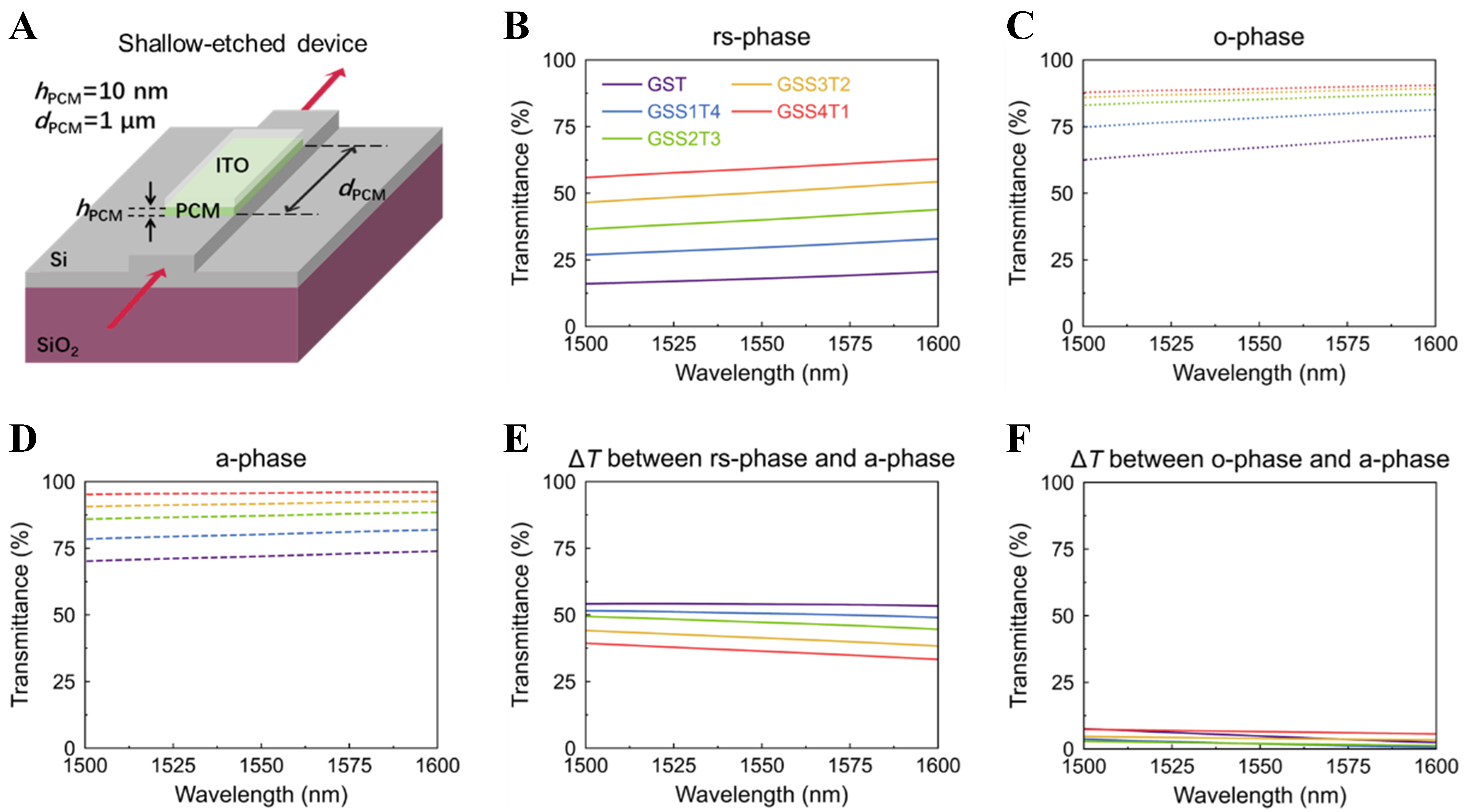
Figure 4. (A) A schematic of the PCM-decorated photonic waveguide. The PCM thickness hPCM and PCM length dPCM being 10 nm and 1 μm, respectively; (B-D) The transmittance spectra of waveguides vs. Se substitution of GST with rs-, o- and a-phase at the telecommunication bands (1,500-1,600 nm) from FDTD simulations. The calculated optical data were used to describe the optical response of GST and Ge2Sb2SexTe5-x (x = 0 to 4); (E) The transmittance contrast (ΔT) of waveguides between the rs-phase and the a-phase; (F) ΔT of waveguides between the o-phase and the a-phase. PCM: Phase-change material; GST: Ge2Sb2Te5; FDTD: finite-difference time-domain.

Journal of Materials Informatics
ISSN 2770-372X (Online)
Follow Us

Portico

All published articles are preserved here permanently:

https://www.portico.org/publishers/oae/

Portico

All published articles are preserved here permanently:

https://www.portico.org/publishers/oae/