

Efficiency enhancement of thermal-evaporated perovskite light-emitting diodes through process optimization and additive engineering
 0
0 Abstract
Thermal evaporation offers precise thickness control and compatibility with large-area processing, making it an attractive route for perovskite light-emitting diodes (PeLEDs). However, evaporated devices have historically shown lower efficiency and stability than solution-processed counterparts. This review summarizes recent progress in enhancing the performance of thermally evaporated PeLEDs through process optimization and additive engineering. Process optimization strategies include tuning precursor ratios, deposition rates, substrate temperatures, post-annealing conditions, and the thickness of emissive and charge-transport layers. Such adjustments improve film crystallinity, exciton confinement, and charge balance while suppressing non-radiative losses. In parallel, organic and inorganic additives have been widely applied to passivate defects, stabilize emissive phases, and enhance operational stability, leading to significant gains in external quantum efficiency. Beyond these approaches, advanced design concepts are emerging. Host-dopant systems enable efficient energy transfer and controlled emission, multi-quantum well structures enhance carrier confinement, and single-source thermal evaporation using solid powder precursors simplifies fabrication and improves reproducibility. These strategies define a pathway toward bridging the performance gap with solution-processed devices. Finally, we highlight applications of evaporated PeLEDs in active-matrix displays, where integration with thin-film transistors demonstrates their promise for scalable, high-resolution display technologies. Broader opportunities in lighting, flexible optoelectronics, and integrated photonics further underscore the versatility of this approach. By consolidating progress in process control, additive engineering, and device design, this review outlines critical directions for advancing thermally evaporated PeLEDs toward commercial viability, combining fundamental insights with practical engineering strategies to achieve efficient, stable, and scalable optoelectronic devices.
Keywords
INTRODUCTION
Metal halide perovskites (MHPs) have attracted significant attention for applications in solar cells[1-6], light-emitting diodes (LEDs)[7-10], sensors[11-13], and other semiconductor devices[14-18] due to their superior optical and electrical properties. In particular, MHPs have demonstrated strong potential as emitting layers for display technologies, owing to their desirable optical properties including narrow full-width at half maximum (FWHM) emission and near-unity photoluminescence quantum yield (PLQY), as well as favorable electrical properties such as low turn-on voltage and high current efficiency[7-9]. The structure of MHPs is typically expressed by ABX3, where A and B are monovalent and divalent cations, respectively, and X is a halide anion such as Cl, Br, or I. As the cation changes, variations in ionic radius, charge balance, and coordination environment arise, which reduce the stability of the ABX3 structure and consequently lead to the formation of alternative structures such as Cs3Cu2X5[19].
The first application of MHPs as emitting layers was reported in 2014 using solution-processed films. Since 2014, the performance of solution-processed perovskite LEDs (PeLEDs) has improved rapidly. Typically, the performance of display devices is evaluated in terms of external quantum efficiency (EQE) and luminance. The initial devices, fabricated using a nanocrystal pinning method with MAPbBr3 (where MA = Methylammonium), achieved an EQE of 0.4% and a luminance of 364 cd·m-2[20]. More recently, record-breaking PeLEDs have demonstrated luminance values of 1,167,000 cd·m-2[21] and EQEs of 28.9%[22] without optical modification, representing more than a 50-fold improvement. Along with these enhancements, efforts toward commercialization have included strategies for pixel isolation and the fabrication of active-matrix devices[23-25]. Nevertheless, the most common solution-processing method spin-coating remains limited in terms of pixelation and scalability.
Thermal evaporation (TE), a conventional physical vapor deposition technique widely employed for alloys[26-30] and organic materials[31,32], offers an alternative fabrication route. Notably, organic LEDs have adopted TE as the primary deposition method for decades in commercial production. TE provides distinct advantages for LED fabrication, including scalability, pixel patterning, and precise thickness control. For PeLEDs, several TE-based strategies have been investigated to achieve uniform perovskite films, such as single-source TE, multi-source TE, and sequential TE. However, compared with solution-processed PeLEDs, TE-based PeLEDs still suffer from inferior performance, primarily due to high defect densities and poor film quality.
In this review, we discuss the fundamental principles of TE for depositing emitting layers and examine the factors that influence the performance of PeLEDs. For example, the TE rate affects grain size[33], while the underlying layer on the substrate can determine the crystallinity of the MHP film[34]. To narrow the performance gap between solution-processed and TE-processed devices, optimization of TE parameters through systematic trial and error is essential. In solution processing, various strategies such as core-shell structure[35-37], doping[38-42], dimensional control[43-47], and additive engineering[48-52] have been widely adopted to enhance PeLED performance. Recently, similar approaches have been applied to TE-based PeLEDs, including the incorporation of additives to improve efficiency. We summarize the methods for achieving uniform MHP films and optimizing device architectures, and we also suggest potential directions for further improving the intrinsic properties of MHPs. Finally, we highlight recent progress in applying TE-based PeLEDs to active-matrix displays and other optoelectronic devices, and we discuss the remaining challenges and outlook. The overall contents were summarized in [Figure 1].
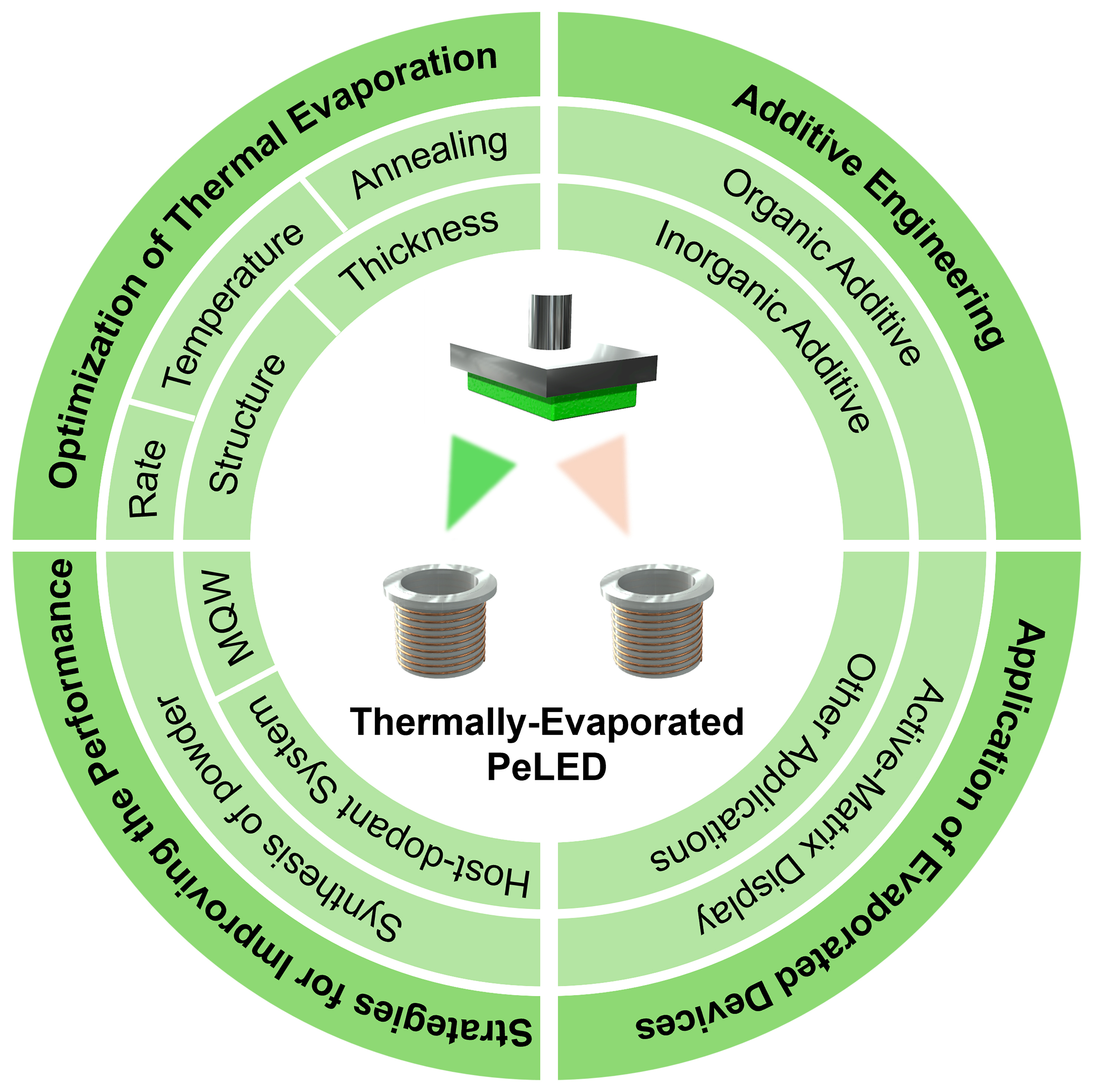
Figure 1. Schematic overview of TE-based PeLED, containing the optimization process, strategies for enhanced performance and applications. TE: Thermal evaporation; PeLED: perovskite light-emitting diode.
FUNDAMENTAL PRINCIPLE FOR TE
In TE of MHPs, formation of thin films generally involves three sequential steps. Initially, in terms of multiple-source TE, Joule heating induces sublimation of precursor materials such as CsX and PbX2 (X = Cl, Br, I), which subsequently diffuse throughout the chamber for evaporation. Upon encountering the relatively cooler substrate, the vapor-phase precursors condense to form a film. The morphology of MHP films is determined by the interaction between adsorbate-adsorbate and adsorbate-substrate interactions, including island growth, monolayer growth, or mixed growth. Among these, the island-growth (Volmer-Weber mode) is most frequently observed, as perovskite-perovskite interactions typically dominate, leading to nucleation of discrete crystals. For application in LEDs, however, these nuclei must continuously exist without a pinhole to ensure efficient charge transport and radiative recombination. Thus, achieving high-quality emission layers necessitates careful optimization of deposition and systematic control over process parameters that critically influence thin-film morphology and uniformity.
Various deposition strategies have been explored for the fabrication of MHP thin films, including dual- or multi-source TE, sequential TE, and single-source TE. Among these, multi-source TE has been one of the most widely researched methods, wherein the precursor components (AX and PbX2, A: Cs, MA; X: Cl, Br, I) are co-evaporated simultaneously. During this process, quartz crystal sensors positioned near each source enable real-time monitoring of the deposition rate, thereby allowing control over the resulting film thickness. However, as multiple sources are operated simultaneously, mutual interference between sensors may lead to reduced accuracy compared to single-source configurations. This technique was first applied to perovskite thin films in 2013 for photovoltaic applications[53]. In the context of LEDs, early studies primarily focused on the green-emitting perovskite APbBr3 (A: Cs, MA), owing to its intrinsic stability. For all-inorganic perovskites, Cs incorporation at the A-site yields CsPbBr3; when the Pb ratio is increased from 1:1 to 1.5:1, the wide-bandgap Cs4PbBr6 phase is formed[54]. However, due to poor film uniformity in the latter case, the stoichiometric 1:1 composition exhibited superior electrical characteristics. PeLEDs based on methylammonium (MA)-containing MAPbBr3 have also been demonstrated, where post-annealing was shown to improve film uniformity[55]. Nevertheless, since post-annealing also heats adjacent charge-transporting layers, careful optimization of layer selection, annealing time, and temperature is required to minimize degradation of charge mobility.
To address the limitations of multi-source TE, particularly the challenges in precise thickness control, sequential deposition methods have been developed[56]. In this method, PbX2 and AX are deposited continuously rather than simultaneously, enabling more accurate control of individual layer thicknesses. However, sequential TE may lead to local compositional variations across layers, necessitating high temperature annealing to achieve sufficient crystallization. This requirement also imposes restrictions on the choice of adjacent charge-transport layers due to potential thermal incompatibility such as multiple-source TEs.
Similar to spin-coating in solution processing where thin-film formation and crystallization occur simultaneously, multi-source TE and sequential TE also produce films while inducing crystallization during the deposition process [Figure 2A]. By contrast, single-source TE involves the prior synthesis of bulk perovskites in solid form, which are subsequently evaporated to directly form thin films, similar to the hot-injection method used for quantum dot synthesis, where a separate film-fabrication step is required after nanoparticle preparation. Solid-state perovskites suitable for this approach are typically prepared either via solution-based synthesis, yielding micro-scale powders or single crystals, or through mechanical methods such as ball milling and high-temperature sintering. Synthesized powders are then placed in a boat or crucible and evaporated under vacuum to deposit thin films with both controlled stoichiometry and precisely tunable thickness. Although this technique has been primarily explored for iodine-based perovskite films, often in the context of photovoltaic applications, research remains comparatively limited relative to multi-source or sequential deposition methods[57].
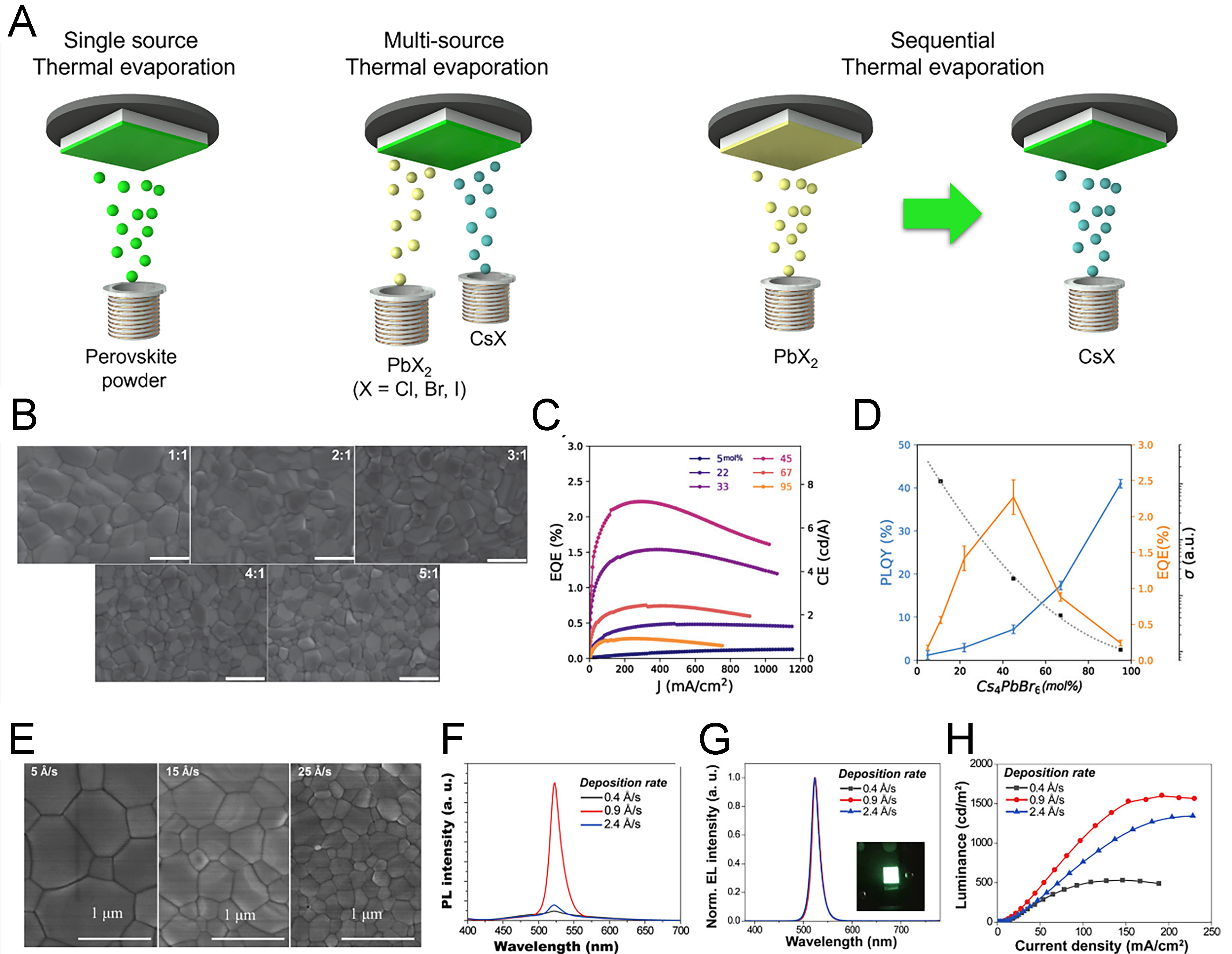
Figure 2. Properties of TE-based MHP films according to ratio of precursor and evaporating rate. (A) Various TE methods for the formation of MHP thin films; (B) SEM images of the MHP films fabricated by TE with varied Cs/Pb ratio[59]. Copyright 2019 AIP publishing; (C) The EQE data of deposited MHP films depending on the different ratio of Cs4PbBr6; (D) PLQY and EQE, and conductivity data according to the ratio of Cs4PbBr6 phase[60]. Copyright 2019 John Wiley & Sons; (E) SEM image of the CsPbBr3 films with different rate of TE[33]. Copyright 2018 John Wiley & Sons; (F) The PL spectra and (G) EL spectra, and (H) luminance data of thermal-evaporated CsPbBr3 from 0.4 to 2.4 Å·s-1[63]. Copyright 2020 American Chemical Society. TE: Thermal evaporation; MHP: metal halide perovskite; SEM: scanning electron microscopy; EQE: external quantum efficiency; PLQY: photoluminescence quantum yield; PL: photoluminescence; EL: electroluminescence.
OPTIMIZATION OF FACTORS AFFECTING TE
During TE, the properties of the resulting thin films can vary significantly depending on multiple factors, including the precursor ratio, deposition rate, substrate temperature, and post-deposition annealing. These parameters collectively influence the crystallinity and phase of perovskite films, which critically determine the performance of the fabricated devices. In this section, we aim to provide a detailed analysis of how each factor impacts film formation and device performance, drawing on recent trends.
The ratio of precursor
The precursors commonly applied for LEDs are typically deposited using CsX and PbX2 sources to form CsPbX3. Early solution-processing research based on spin-coating revealed that introducing a higher amount of MABr relative to PbBr2 in the precursor solution could effectively suppress Pb-related defects caused by uncoordinated Pb atoms, thereby yielding improved perovskite films[58]. Similarly, in dual-source TE, attempts were made to utilize a higher CsBr ratio relative to PbBr2. When Poly(N,N’-bis-4-butylphenyl-N,N’-bisphenyl)benzidine (poly-TPD) was used as a hole-transport layer and the CsBr:PbBr2 ratio was varied between 1:1 and 1.5:1, devices fabricated with the 1.5:1 ratio showed inferior performance due to surface inhomogeneity of the films. Scanning electron microscope (SEM) characterization confirmed that the 1:1 film exhibited pinhole-free surfaces, whereas the 1.5:1 film displayed irregular morphology[53]. However, as the optimization was incomplete, these devices exhibited a higher turn-on voltage compared with solution-processed counterparts, which showed a threshold voltage of approximately 3 V.
Subsequent research extended the CsBr:PbBr2 ratio up to 5:1[59]. Despite the high CsBr content, no significant changes in crystal structure were detected. As shown in Figure 2B, the increasing ratio led to a reduction in grain size, which was favorable for forming films with enhanced carrier confinement beneficial for LED applications. Unlike earlier research, devices were fabricated entirely by TE, with an indium tin oxdie (ITO)/MoO3/Tris(4-carbazoyl-9-ylphenyl)amine (TCTA)/CsPbBr3/2,2’,2’’-(1,3,5-Benzinetriyl)-tris(1-phenyl-1-H-benzimidazole) (TPBi)/LiF/Al structure. At a 5:1 ratio, the device achieved a luminance of
In addition to precursor ratio engineering, other studies optimized film properties based on the molar fraction of the Cs4PbBr6 phase within the emissive layer, as well as by tuning the film thickness[60]. In this case, when CsPbBr3 and Cs4PbBr6 phases coexisted, carriers migrated through two distinct conductive channels and the excessive thickness of the emissive layer increased resistance or introduced shunt pathways; thus, an optimal thickness of 60 nm was employed. As illustrated in Figure 2C, the maximum EQE was achieved when the Cs4PbBr6 content reached 45 mol%, where the moderate presence of Cs4PbBr6 effectively regulated the CsPbBr3 grain size and enabled spatially confined carrier transfer. Conversely, excessive Cs4PbBr6 exhibited insulating behavior, leading to the discrepancy between the ratios that yielded maximum EQE and those that yielded the highest PLQY [Figure 2D]. The optimized device exhibited a luminance of 53,486 cd·m-2 and an EQE of 2.5%. Based on various research findings, employing a higher Cs ratio relative to Pb during deposition is beneficial for mitigating Pb-induced defect formation and facilitating the controlled incorporation of the Cs4PbBr6 phase; nevertheless, attention is required in emissive layer fabrication to prevent excessive Cs4PbBr6 formation, which could impart an undesirable insulating effect.
The rate of TE
During TE, one of the critical factors influencing thin-film characteristics is the deposition rate. While organic-inorganic MHPs are commonly applied to photovoltaic devices, TE has also been explored for fabricating inorganic CsPbBr3 films, which are thermally stable but difficult to form into uniform layers[32].
In thermally evaporated MHP films, grain-size control emerges as a key parameter that is strongly influenced by the TE rate. Unlike perovskite solar cells, where large grains and reduced grain-boundary density are typically targeted to promote long-range carrier transport and efficient charge collection, PeLEDs often benefit from a more finely tuned microstructure. Moderately small, uniformly distributed grains can localize charge carriers and excitons, thereby enhancing the probability of radiative recombination while suppressing nonradiative pathways associated with deep trap states and extended defect networks at grain boundaries. In TE processes, the grain size and morphology can be systematically engineered by adjusting the TE rate. A high TE rate induces a large nucleation density, and the numerous nuclei within a limited area result in a small grain size. Although such small grains are advantageous for PeLEDs, MHP films composed of very small grains can suffer from incomplete coverage and the formation of pinholes. Consequently, optimizing grain size by combining fast TE with sufficiently robust post-annealing conditions represents an essential design strategy for achieving superior TE-based PeLED performance[61,62]. Similar to the previous approach, after optimizing the precursor ratio, the effect of deposition rate was investigated by forming films at 5, 15, and 25 Å·s-1.
Although no phase transition was observed as a function of deposition rate, the crystallographic orientation was strongly affected. These changes in crystallinity ultimately altered the grain size, and a deposition rate of 5 Å·s-1 fabricated large grains suitable for photovoltaic applications [Figure 2E][33]. In contrast, thin films with smaller grains are desirable to facilitate spatially confined carrier transport for LEDs, implying that higher deposition rates are more advantageous.
The crystallinity dependence on TE rate can be attributed to the increased nucleation density at the substrate surface under faster deposition conditions. In this context, Shin et al. evaluated the deposition-rate dependence of CsPbBr3 films prepared for vacuum-deposited LEDs[63]. Emitting layers were fabricated at deposition rates of 0.4, 0.9, and 2.4 Å·s-1, and the best optoelectronic properties were obtained at 0.9 Å·s-1 [Figure 2F-H]. Although a smaller grain size was expected at 2.4 Å·s-1, rapid deposition of PbBr2 resulted in the formation of microscale grains caused by residual gases. The grain-size inhomogeneity hindered spatial control of carrier transport and degraded device performance. By employing the optimized deposition rate, the improved device successfully achieved a three-fold enhancement in luminance, reaching 1,607 cd·m-2.
In summary, while relatively high deposition rates are generally required to fabricate emitting layers suitable for LEDs, excessively fast evaporation of PbX2 can induce grain-size nonuniformity, necessitating careful optimization of the rate. Further studies are also required to determine whether performance differences arise under single-source or sequential TE when varying the deposition rate.
The temperature of substrate
Substrate temperature during TE has been shown to exert influence over film nucleation and growth, thereby dictating the structural and optoelectronic properties of the resulting emitting layers. Elevated substrate temperatures generally promote enhanced surface diffusion of adatoms, leading to improved crystallinity, enlarged grain sizes, and reduced defect densities, which in turn contribute to higher charge carrier mobility and more balanced injection. However, excessive heating can trigger undesirable phase segregation, lattice strain, or interfacial reactions, particularly in MHPs where volatile species are prone to re-evaporation[64,65]. Recent research demonstrates that optimized substrate temperatures affect the MHP film to smoother morphologies, reduced trap-assisted recombination, and enhanced luminance in CsPbBr3- and mixed-halide based PeLEDs, whereas insufficient thermal activation often results in rough, polycrystalline films with inferior current efficiency. Furthermore, optimization of substrate temperature has been correlated with modifications in preferred crystallographic orientation, which critically affects light outcoupling and performance of emission. The temperature of the substrate is not merely a processing variable but an active parameter for engineering microstructure and exciton dynamics in vacuum-deposited LEDs.
In addition to optimizing the deposition rate, several studies have reported improved performance in LEDs through careful control of substrate temperature. When the substrate temperature was varied from 30 to
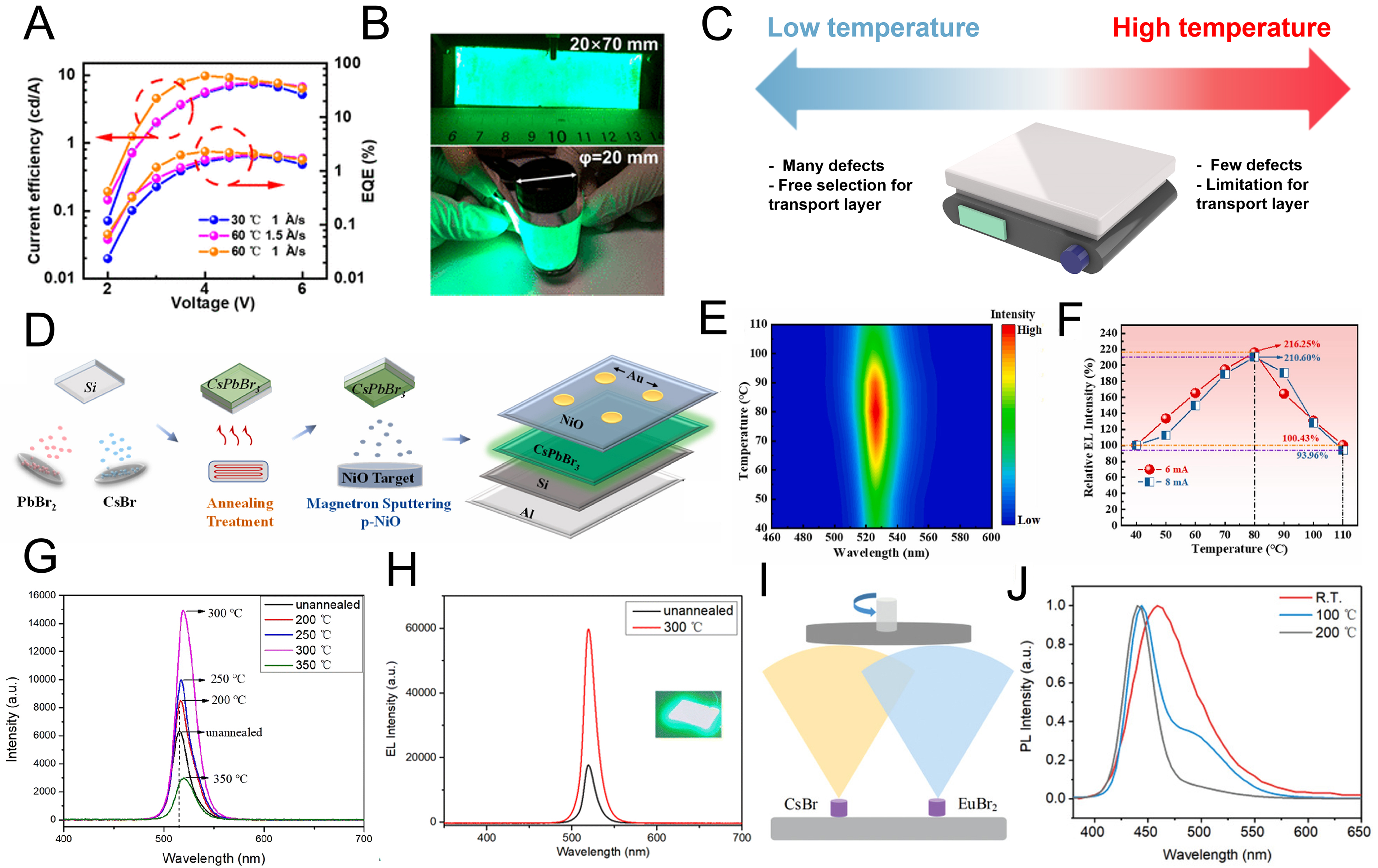
Figure 3. Characterizations of PeLED depending on the temperature of substrate and post-annealing. (A) Current efficiency and EQE of PeLEDs fabricated by TE with varied substrate temperature and rate; (B) The image of deposited MHP films with large substrate and flexible substrate[66]. Copyright 2020 American Chemical Society; (C) The scheme of illustrating the effect depending on the temperature of substrate; (D) Scheme of the process for fabricating the PeLED with high temperature annealing; (E) PL spectra of CsPbBr3 post-annealing at 240 °C depending on the measured temperature; (F) Graph for relative EL intensity according to temperature from 40 to 110 °C[72]. Copyright 2023 Elsevier; (G) PL spectra of CsPbBr3 films with post-annealing from 200 to 350 °C and pristine film; (H) PL spectra of CsPbBr3 films with post-annealing at 300 °C and pristine film[73]. Copyright 2023 Royal Society of Chemistry; (I) The image of fabricating CsEuBr3 with multi-source TE, and (J) PL spectra depending on the post-annealing from RT to 200 °C[74]. Copyright 2021 John Wiley & Sons. PeLED: Perovskite light-emitting diode; EQE: external quantum efficiency; TE: thermal evaporation; MHP: metal halide perovskite; PL: photoluminescence; EL: electroluminescence; RT: room temperature.
In another study, substrates were thermally treated from room temperature up to 120 °C during deposition to fabricate red, green, and blue devices[67]. Compared to room-temperature deposition, elevated substrate temperatures reduced defects and promoted the formation of grains with uniform size, leading to enhanced device performance. However, excessive heating to 120 °C increased surface roughness and degraded device efficiency. The optimal condition was identified at 100 °C, under which all three emission colors were successfully realized and characterized. Similar approaches have also been applied to lead-free MHP where CsSnBr3 films were deposited while maintaining substrate temperature at room temperature, 50, 75, and
Conversely, lowering the substrate temperature below room temperature has also been explored for blue LED fabrication. When PbBr2, CsBr, and CsCl were co-deposited at a slow rate, substrates held at room temperature and -10 °C were compared[69]. The lower substrate temperature facilitated greater nucleation density, enabling rapid formation of uniform films and allowing radiative recombination to occur at lower carrier densities. As a result, blue LEDs fabricated at -10 °C achieved a luminance of 1,640 cd·m-2, an EQE of 7.2%, and stable operation for approximately 7 min.
This research demonstrates that elevated substrate temperature promotes uniform grain formation and helps mitigate boundary defects, but excessively high temperature can induce film non-uniformity and increase defect density. In contrast, low substrate temperature enables dense nucleation and uniform small-grain films, though they require specialized deposition systems with cooling capability. The temperature-dependent changes in film characteristics are summarized in Figure 3C.
The optimization for annealing
Post-annealing has been widely recognized as a crucial strategy for improving the structural and optoelectronic quality of TE-based perovskite films and their corresponding LEDs. Post-annealing on MHPs facilitates enhanced atomic diffusion, which not only promotes improved crystallinity and enlarged grain sizes but also reduces defect densities that act as nonradiative recombination centers. Research has demonstrated that appropriately chosen annealing temperature and time lead to smoother morphologies, reduced trap states, and superior optical stability, with films retaining a high fraction of their luminescence intensity after extended storage[70]. At the device level, optimized annealing conditions resulted in lower operating voltages, higher luminous efficiencies, and longer operational stability in PeLEDs. Nevertheless, excessive annealing temperature or prolonged heating can induce phase segregation, or interfacial degradation, emphasizing the requirement for precise optimization of the process parameters. Collectively, Research highlighted post-annealing as an indispensable tool for structural engineering, enabling both improved performance and long-term stability of TE-based PeLEDs.
After the TE, post-annealing at various temperatures has been employed to optimize thin-film properties. Huang et al. maintained a dual-source TE using CsBr and PbBr2 at a deposition rate of 0.4 Å/s, followed by annealing at 60, 90, and 120 °C. They observed that grain size increased with annealing temperature up to
At higher annealing temperatures, organic charge transport layers may undergo structural deformation; thus, devices are often fabricated without a transport layer or by employing inorganic transport layers. As shown in Figure 3D, an LED with an Al/Si/CsPbBr3/NiOx/Au structure was fabricated on a thermally robust silicon substrate using dual-source TE of CsBr and PbBr2, followed by annealing at 240 °C[72]. Compared with solution-processed films, vacuum deposition offers the advantage of enabling high-quality thin-film growth even on inorganic substrates. The electrical performance of the device was examined by applying bias under temperatures ranging from 40 to 110 °C. As shown in Figure 3E, the electrical properties improved up to
Using a similar dual-source TE with CsBr and PbBr2, researchers have also fabricated composite CsPbBr3-Cs4PbBr6 thin films by tuning precursor ratios[73]. The optimal film was obtained at a Cs/Pb ratio of 1.34, showing superior optoelectronic performance. Upon annealing from 200 to 350 °C [Figure 3G], variations in photoluminescence (PL) intensity and peak position were observed, resulting in the effective defect passivation and grain growth. The red shift in PL emission was attributed to enlarged grain size. LEDs with an Ag/n-type silicon (n-Si)/MHP/NiO/ITO configuration exhibited a luminance of 957 cd·m-2, and at 300 °C, both enhanced EL intensity and red shift occurred [Figure 3H]. Notably, the devices retained more than 90% of their initial performance after 6 h of continuous operation, underscoring the effectiveness of defect suppression.
The dual-source TE has also been extended to lead-free perovskite blue emitters[74]. CsEuBr3 films were fabricated via dual-source TE of CsBr and EuBr3 [Figure 3I]. Unlike conventional lead-free perovskites, which typically exhibit broad full-width half maximum (FWHM) due to limited defect tolerance, Eu2+ ions, comparable to Pb2+, contribute to both the valence band maximum (VBM) and conduction band minimum (CBM), thereby facilitating charge transport and yielding a narrow FWHM of ~30 nm. A comparison of samples without annealing and with annealing at 100 and 200 °C [Figure 3J] revealed behavior distinct from that of CsPbBr3, while CsPbBr3 exhibits a red shift upon annealing due to grain growth, CsEuBr3 shows a blue shift, which is attributed to enhanced crystallinity and bulk CsEuBr3 formation at 100 °C. A shoulder peak near 515 nm emerged at 100 °C due to defect states from insufficient thermal energy; however, the peak disappeared after annealing at 200 °C, leaving a dominant deep-blue emission at 448 nm.
Single-source TE using bulk CsPbBr3 powder, rather than separate CsBr and PbBr2 precursors, has also been reported[34]. Post-deposition annealing at elevated temperatures from room temperature to 400 °C yielded uniform thin films. Owing to the high annealing temperature, no charge transport layer was employed, and devices with a simple ITO/CsPbBr3/C configuration were fabricated. The optimized 350 °C annealing produced devices with a low turn-on voltage of 2.92 V and a luminance of 14,079 cd·m-2. While post-annealing is essential to promote grain growth otherwise insufficient during TE, excessively high annealing temperature may degrade device performance due to the low glass transition temperature of organic layers. Therefore, careful optimization of annealing conditions and device architecture is crucial for achieving high-performance TE-based PeLEDs[75].
The modification of thickness and structure
The thickness of the emitting layer and the optimization of device structure have emerged as particularly decisive factors for fabricating superior TE-based PeLEDs[76]. Research on CsPbBr3 nanocrystal films demonstrated that careful control of the emitting layer thickness strongly influences film morphology, PL intensity, and carrier dynamics[77]; for example, films around 40 nm exhibited enhanced luminescence and longer carrier lifetimes, translating into higher EQE compared with thinner or thicker counterparts. Equally important, the conscious engineering of device structures through the selection and modification of charge transport layers, adjustment of energy-level alignments, and incorporation of interfacial passivation strategies has been shown to significantly improve charge injection balance, suppress non-radiative recombination, and enhance operational stability[78-81]. The modulation of these factors indicates that a synergistic approach combining precise thickness control with rational structural design is crucial for advancing the efficiency and reliability of TE-based PeLEDs, and provides guiding principles for the development of next-generation high-performance devices.
The key factor influencing the electrical properties of LEDs is the thickness of the emitting layer[82]. In solution-processed perovskite devices, performance was found to vary significantly with film thickness, typically in the range of 30-100 nm. Optical simulations confirmed that changes in emissive-layer thickness modify the distribution of outcoupled modes, thereby affecting the EQE[83]. Similarly, in LED with thermally evaporated CsCu2I3 metal halide luminescent materials, the device performance was also strongly dependent on the emitting-layer thickness[84]. CsCu2I3 is a perovskite whose structure differs from the conventional ABX3 MHP framework, and it can be regarded as the result of a change in the most stable structure caused by the smaller ionic radius of Cu compared with Pb in the prototypical MHP CsPbBr3, as well as differences in charge balance. CsCu2I3 thin films were fabricated via dual-source TE of CsI and CuI. This perovskite exhibits excellent stability, a high PLQY, and the additional advantage of being non-toxic due to the absence of lead. When the emitting-layer thickness varied from 40 to 160 nm, the fabricated LEDs showed comparable turn-on voltages; however, substantial differences were observed in EL spectra linewidths and luminance. For example, devices with an optimal thickness of 60 nm exhibited more than four times higher luminance compared with those with 160 nm thickness and a reduction in FWHM of approximately 60 nm. In all devices, the EL peak was red-shifted relative to the PL peak and showed spectral broadening, which was attributed to iodine ion migration and subsequent cluster formation. Compared with solution processing, systematic studies on the influence of emitting-layer thickness in TE-based PeLEDs remain limited. Therefore, further investigations into the optical and electrical properties of such thickness- dependent effects are needed to establish reliable design guidelines for high-performance TE-based devices.
The properties of TE-based MHP layers are also strongly affected by the underlying substrate layers, prompting extensive studies on the use of diverse organic and inorganic interlayers beyond those commonly employed in solution-processed devices. Compared with solution processing, the absence of solvents allows the use of a wider variety of charge-transport layers; however, layers located above or below the emitting layer can induce charge imbalance or unwanted nonradiative recombination caused by interfacial defects. To control such defects and improve device performance, strategies such as treating the evaporation-based emitting layer with a phenethylammonium bromide (PEABr) solution have been proposed[85]. For improving the interface between the hole transport layer (HTL) and emitting layer, Li et al. fabricated devices by dual-source evaporation of CsBr and PbBr2, optimizing the precursor ratio to form CsPbBr3-Cs4PbBr6 composites[86]. Continuous thermal annealing using graphite blocks, a 50 °C hotplate, and a 200 °C hotplate revealed that treatments between 72-131 °C were most effective. Based on this process, the hole injection layers poly(3,4-ethylenedioxythiophene) polystyrene sulfonate (PEDOT:PSS), NiOx, and LiF were compared. PL decay measurements [Figure 4A] indicated comparable lifetimes for LiF and NiOx, suggesting low defect densities at the perovskite-interlayer interface. In contrast, PEDOT:PSS exhibited markedly shorter lifetimes, pointing to significant defect formation. Interestingly, despite its poorer interfacial quality, PEDOT:PSS yielded higher electrical performance than LiF [Figure 4B and C], which was attributed to its energy band alignment effectively blocking electron leakage. NiOx, however, demonstrated superior interfacial and electrical properties compared to both materials, suppressing electron backflow and enabling excellent hole injection, ultimately delivering 9,442 cd·m-2 luminance and 3.26% EQE.
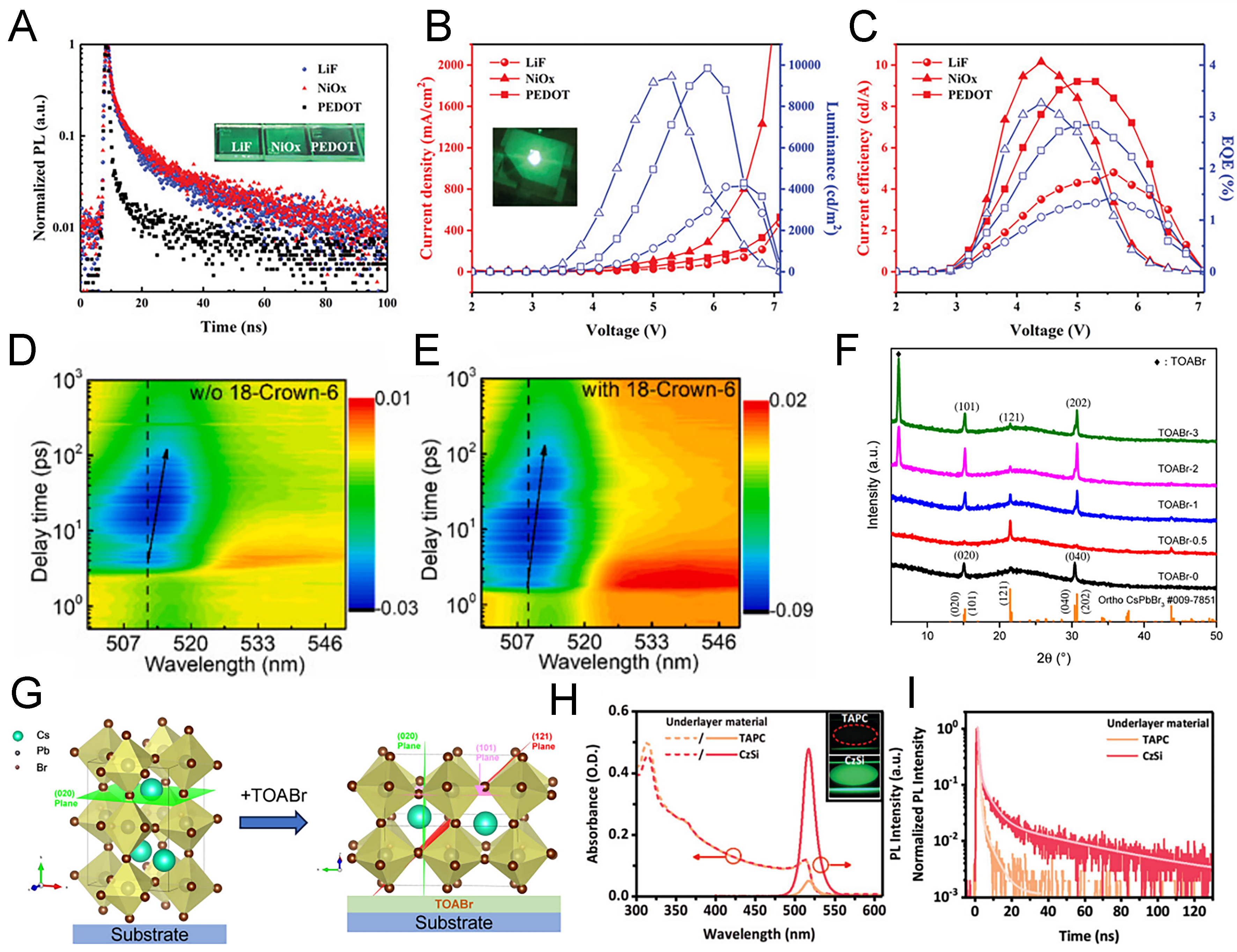
Figure 4. Characteristics depending on the pre-deposited layer before perovskite deposition. (A) PL decay curves with different vacuum-deposited hole transport layers; (B) current density and luminance data with varied transport layers; (C) current efficiency and EQE depending on the hole transport layer[86]. Copyright 2019 John Wiley & Sons; (D and E) transient absorption spectra with or without an 18-crown-6 layer[87]. Copyright 2022 Elsevier; (F) XRD patterns as a function of TOABr concentration pre-deposited before CsPbBr3 deposition; (G) illustration of CsPbBr3 crystal evolution with TOABr treatment[88]. Copyright 2023 American Chemical Society; (H) UV-vis and PL spectra with TAPC or CzSi as charge transport layers, and (I) PL decay curves of CsPbBr3 deposited on two different charge transport layers[89]. Copyright 2023 John Wiley & Sons. PL: Photoluminescence; EQE: external quantum efficiency; XRD: X-ray diffraction; UV-vis: ultraviolet-visible spectroscopy; TOABr: tetraoctylammonium bromide; TAPC: 1,1-bis[(di-4-tolylamino)phenyl]cyclohexane; CzSi: 9,9’-spirobifluorene-based carbazole derivative.
To mitigate the poor interfacial quality associated with PEDOT:PSS, 18-crown-6, an organic molecule widely used in solution-processed devices, was introduced at the perovskite-PEDOT:PSS interface[87]. This treatment improved conductivity, suppressed surface defects, and inhibited the formation of insulating Cs4PbBr6 phases, thereby enhancing operational stability. Transient absorption measurements [Figure 4D and E] confirmed reduced band-tail states and minimized red-shift of transient bleach minima, evidencing effective defect passivation. The optimized devices achieved 15,717 cd·m-2 luminance and 1.02% EQE.
Inorganic interfacial modification has also proven effective. For example, deposition of tetraoctylammonium bromide (TOABr) between NiLiOx and perovskite layers improved film orientation and grain boundary[88]. TOABr, with its four long alkyl chains, promoted preferential growth along the (101) and (020) orientations without introducing secondary phases [Figure 4F]. Excessive deposition marked as TOAB-2 and TOAB-3 led to TOABr impurity peaks, establishing TOAB-1 as the optimal condition. The structural improvements, evidenced in X-ray diffraction (XRD) and morphology analyses [Figure 4G], resulted in device performance of 11,133 cd·m-2 luminance and 1.24% EQE in ITO/NiLiOx/TOABr/CsPbBr3/TPBi/LiF/Al structures. In addition, materials widely employed in organic LEDs have been successfully adapted to PeLEDs. As illustrated in Figure 4H, emissive layers based on optimized CsPbBr3-Cs4PbBr6 composites were combined
These studies demonstrate that beyond deposition rate and substrate temperature, the choice and treatment of pre-deposited transport layers critically determine the optoelectronic properties of TE-based perovskite films. Optimal selection and engineering of both organic and inorganic interlayers, combined with appropriate substrate and post-annealing conditions, are indispensable for realizing high-performance TE-based PeLEDs.
ADDITIVE ENGINEERING
The integration of additives into TE-based perovskite layers has emerged as a powerful strategy to fabricate the MHP thin-film, modulate defects, and enhance optoelectronic performance. Unlike solution processing, where additives are directly injected and interact dynamically during nucleation and growth, the incorporation of organic and inorganic additives in TE must be carefully designed to accommodate the unique kinetics and energetics of vapor-phase film formation.
Organic additive
Organic molecules play diverse roles in regulating film crystallization, passivating defects, and tuning interfacial energetics. Small organic cations and functional ligands such as amines, phosphonic acids, and conjugated aromatic rings have been demonstrated to stabilize low-dimensional perovskite phases during deposition, thereby mitigating non-radiative recombination pathways. For instance, incorporation of PEABr[90-92] or carbazole-based molecules[93-95] has been shown to suppress halide vacancies and control vertical phase distribution, leading to improved film uniformity and enhanced efficiency. PEABr has been most widely employed as an organic spacer in quasi-2D MHPs, which can be considered as 3D MHPs doped with 2D MHP domains. Quasi-2D perovskites exhibit higher exciton binding energy than conventional 3D counterparts and show an n-phase distribution that depends on the number of perovskite layers sandwiched between organic spacers[Figure 5A], where larger n-phases possess smaller bandgaps. Taking advantage of these bandgap differences, a quantum-well structure can be formed, enabling improved charge transfer from wider-bandgap to narrower-bandgap regions and thus enhanced electrical characteristics. However, when multiple n-phases coexist, the bandgap variation can broaden the FWHM and inefficient energy or charge transfer may deteriorate the device performance; therefore, it is crucial to form an emitting layer with a uniform n-phase distribution. To this end, extensive studies have been conducted on the incorporation of various organic additives containing COO- groups to improve phase uniformity and optoelectronic properties[44,96,97]. In addition, as shown in Figure 5A, point-defect passivation and grain-boundary improvement via halide salts, as well as the interaction between phosphine oxide groups and Pb2+ to enhance the perovskite layer properties, represent key roles of such organic additives in quasi-2D perovskite systems.
PEABr is widely applied in solution-processed MHPs to synthesize low-dimensional structures as mentioned above, and similar approaches have been extended to TE to enhance perovskite thin films[98]. In one study, PbBr2 was first deposited, followed by the co-evaporation of MABr and PEABr with varying ratios as illustrated in [Figure 5B]. While MAPbBr3 fabricated by TE alone exhibited poor optical properties, the incorporation of a small amount of PEABr improved its optical properties. However, excessive PEABr content induced the formation of a (PEA)2PbBr4 (PEA = phenethylammonium), resulting in blue rather than green emission. XRD analysis [Figure 5C] confirmed that a MA/PEA ratio of 1:0.25 fabricated pure MAPbBr3, whereas a 1:0.5 ratio led to the coexistence of MAPbBr3 and (PEA)2PbBr4. Importantly, at the optimal 1:0.25 ratio, pinhole defects were effectively suppressed, while the reduced refractive index minimized the mismatch with adjacent transport layers, thereby enhancing light outcoupling. Consequently, the devices achieved a luminance of 6,200 cd·m-2 and an EQE of 0.36% [Figure 5D], outperforming other PEABr ratios. This demonstrated the potential of controlled PEABr incorporation in modifying film quality and device efficiency.
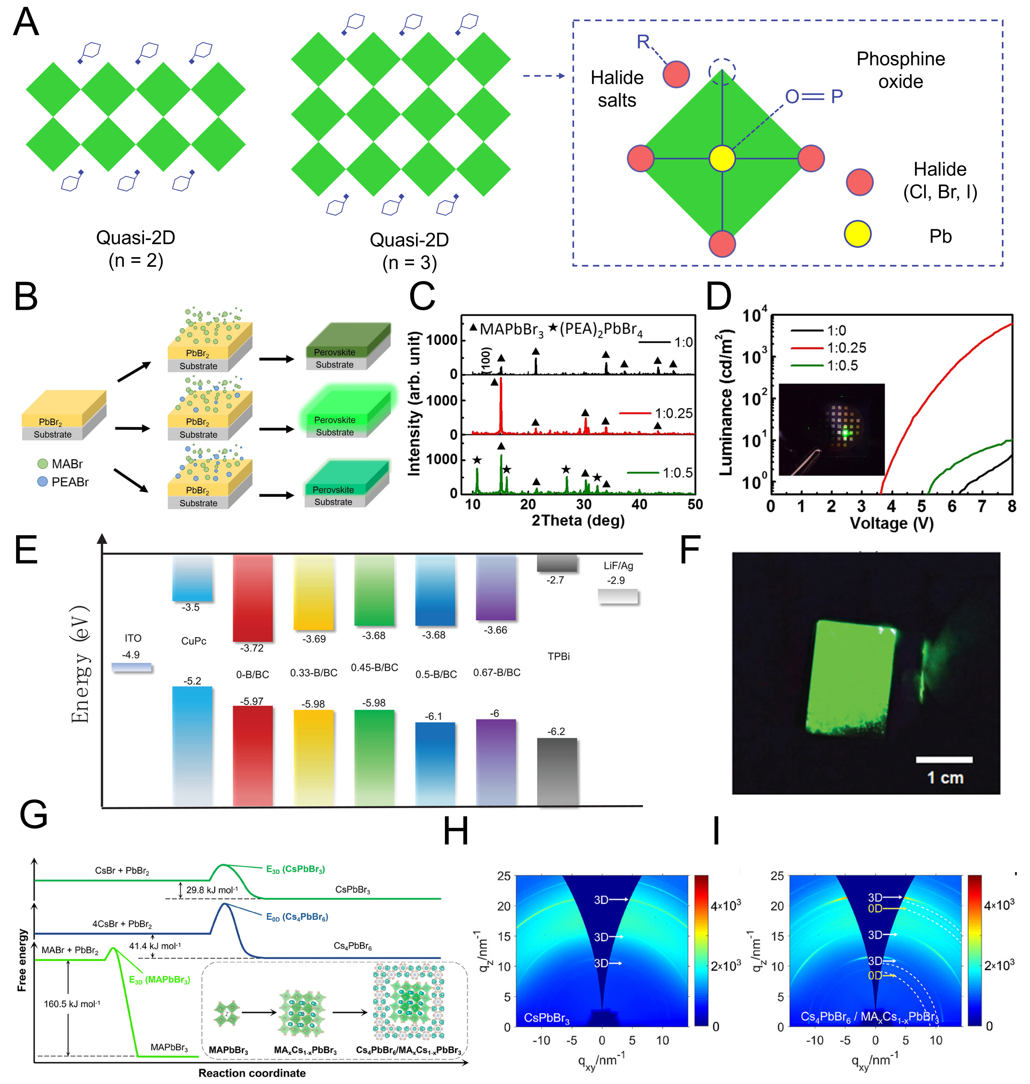
Figure 5. Improvement of perovskite films and devices by organic additives. (A) The structure of quasi-2D MHPs with organic spacer (left) and the effect of diverse organic additive (right); (B) Schematic illustration of PEABr incorporation into MAPbBr3; (C) XRD patterns with varying MABr:PEABr ratios from 1:0 to 1:0.5; (D) luminance-voltage characteristics of LEDs fabricated with different MABr:PEABr ratios[98]. Copyright 2017 American Chemical Society; (E) energy level alignment of perovskite layers with different BABr contents for quasi-2D structures; (F) electroluminescence image of a 0.5B/BC-based LED under 5 V bias[100]. Copyright 2020 John Wiley & Sons; (G) mechanism of formation energies for CsPbBr3 and Cs4PbBr6 with or without MABr during CsPbBr3 fabrication; (H) GIWAXS pattern of pristine CsPbBr3, and (I) GIWAXS pattern of CsPbBr3 with MABr incorporation[101]. Copyright 2025 John Wiley & Sons. MHPs: Metal halide perovskites; PEABr: phenethylammonium bromide; MAPbBr3: methylammonium lead bromide; XRD: X-ray diffraction; LED: light-emitting diode; BABr: butylammonium bromide; GIWAXS: grazing-incidence wide-angle X-ray scattering; MABr: methylammonium bromide.
Beyond MAPbBr3, the formation of quasi-2D perovskites via PEABr incorporation has also been investigated, enabling multi-quantum-well (MQW) structures that enhance both optical and electrical properties[99]. PEABr was introduced during CsPbBr3 deposition, and subsequent thermal annealing promoted grain growth, producing uniform, defect-suppressed films. Efficient exciton transfer from low- to high-dimensional domains was confirmed, leading to improved device performance. Optimized devices, incorporating modified charge transport layers, achieved an EQE of 6.5% and luminance of 7,400 cd·m-2.
In contrast to the aromatic PEABr, alkyl-chain ammonium additives have been utilized to improve low-dimensional MHPs and grain boundaries. Sequential TE of CsBr, PbBr2, and n-butylammonium bromide (BABr) produced films with quasi-2D/3D coexisting, resembling a core-shell morphology[100]. By tuning the BABr/(BABr + CsBr) ratio between 0 and 0.67 and applying post-annealing at 160 °C for 5 min, the most uniform nanoflake-like morphology was obtained at a ratio of 0.45. As shown in Figure 5E, X-ray photoelectron spectroscopy (XPS) and Tauc plot analysis confirmed favorable band alignment, and the fabricated LEDs [ITO/Copper(II) phthalocyanine (CuPc)/MHP/TPBi/LiF/Ag] exhibited 8,400 cd·m-2 luminance and 5.3% EQE and the devices displayed bright EL at 5 V [Figure 5F]. These results indicate that the high annealing temperature imposes limitations on the choice of hole transport materials, such as CuPc. This highlights the trade-off between film crystallinity and process compatibility in TE systems.
Another strategy involved the incorporation of MABr during CsPbBr3 growth to simultaneously achieve defect passivation and crystallinity enhancement[101]. The low formation energy of MAPbBr3 enabled it to act as nucleation sites, upon which CsPbBr3 crystals grew. Meanwhile, excess CsBr and PbBr2 facilitated the formation of Cs4PbBr6 around CsPbBr3 domains, further reducing defects and improving film quality. As shown in Figure 5G, crystallization followed an energy hierarchy from MAPbBr3 to CsPbBr3 to Cs4PbBr6. PL spectra confirmed enhanced intensity and narrower FWHM upon MABr incorporation, while grazing-incidence wide-angle X-ray scattering revealed characteristic ring patterns at q = 0.97 and 2.08 Å-1, indicating randomly oriented Cs4PbBr6 domains [Figure 5H and I]. Based on this, LEDs using mixed Cs4PbBr6/MAxCs1-xPbBr3 films achieved a record-high luminance of 246,211 cd·m-2 and an EQE of 5.97%.
Beyond ammonium-based spacers, bis[2-[(oxo)diphenylphosphino]phenyl] ether (DPEPO) was co-deposited with PbBr2 and CsBr to delay crystallization, thereby forming uniform films[102]. Phosphine oxide groups interact with Pb2+ ions through P=O coordination, stabilizing local bonding and mitigating trap formation[103,104]. With DPEPO treatment, Pb-ion coordination was strengthened, grain boundaries were improved, and trap density was reduced, enabling uniform film growth. This strategy led to devices exhibiting outstanding performance, with luminance of 35,083 cd·m-2 and an EQE of 16.91%. These results underline the promise of functional phosphine oxide additives in defect suppression and film uniformity control.
Research has also been extended to blue and red devices, which typically show inferior performance compared to their green counterparts[105]. For instance, post-deposition treatment with metformin hydrochloride improved film uniformity and defect passivation in multi-source TE-based CsBr/CsCl/PbBr2 films[106]. This approach not only enhanced electrical properties but also effectively mitigated anion exchange, a key issue compromising color purity in blue LEDs, thus ensuring spectral stability under high bias. Similarly, post-deposition treatment with Phenethylammonium chloride (PEACl) followed by GABr yielded synergistic improvements[107]. While PEACl incorporation alone induced a blue shift in PL spectra due to Cl- incorporation [Figure 6A], the subsequent addition of GABr led to a slight red shift from Br- incorporation [Figure 6B]. The cations, consisting of PEA+ and Guanidinium (GA+), did not alter the perovskite crystal structure but contributed defect passivation by donating electrons from N–H bonds to undercoordinated Pb2+. As a result, the devices exhibited a twofold increase in EQE, achieving 6.09% [Figure 6C].
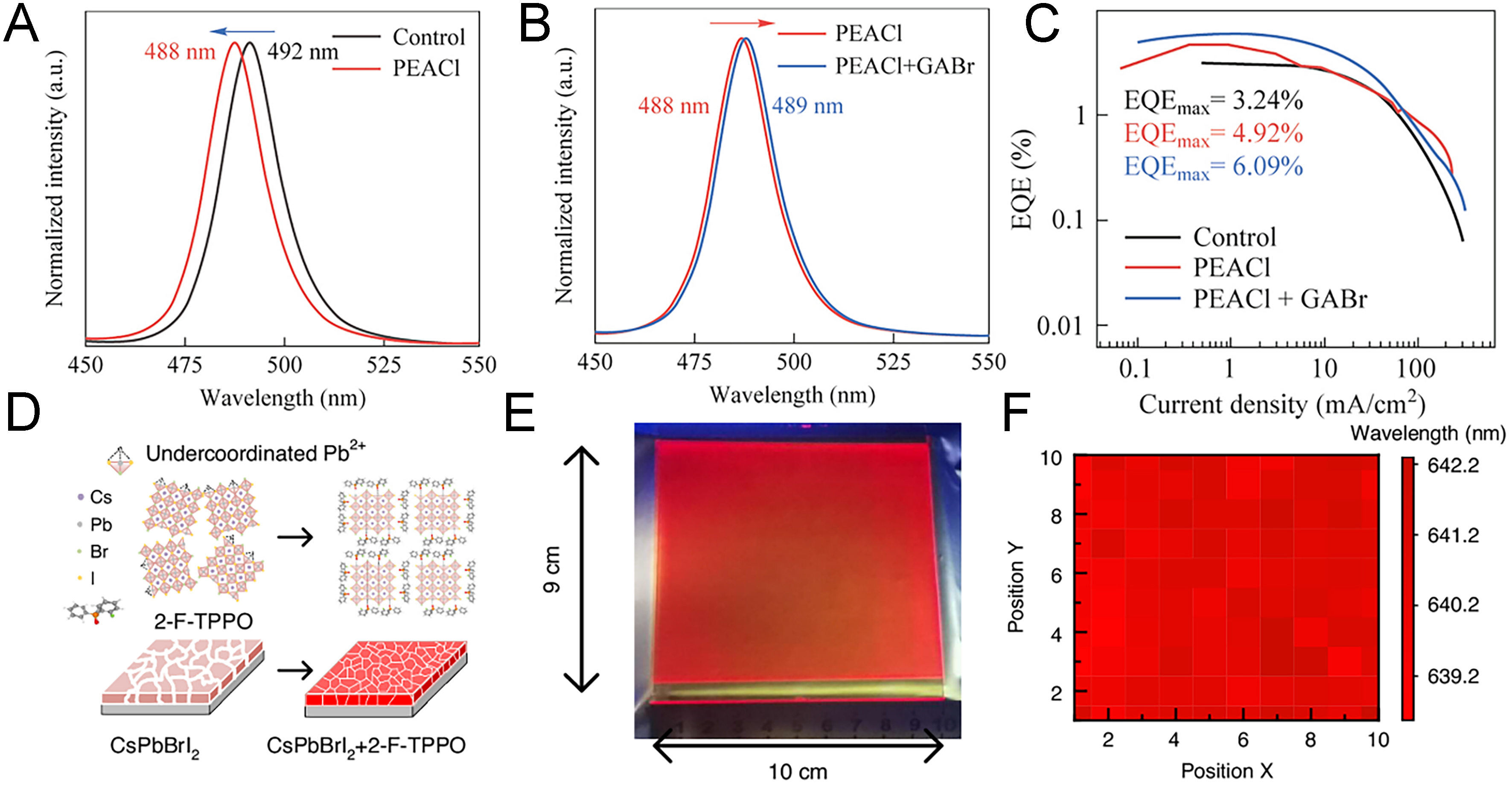
Figure 6. Data related to performance improvement by organic additives. (A) PL spectra changes upon incorporation of PEACl into CsPbBr3; (B) PL spectra of CsPbBr3 treated with PEACl only and with both PEACl and GABr; (C) EQE vs. current density of pristine CsPbBr3, PEACl-treated, and GABr-treated films[107]. Copyright 2025 Springer; (D) schematic illustration of perovskite modification in CsPbBrI2 upon addition of 2-F-TPPO; (E) optical image of a large-area perovskite film deposited by vacuum evaporation, and (F) PL peak position of large-area CsPbBrI2:2-F-TPPO films[108]. Copyright 2025 Springer. PL: Photoluminescence; PEACl: phenethylammonium chloride; GABr: guanidinium bromide; EQE: external quantum efficiency; TPPO: triphenylphosphine oxide.
Finally, fluorinated organic additives have been introduced to red devices. For example, 2-F-triphenylphosphine oxide (2-F-TPPO) combined the defect-passivation capabilities of P=O moieties with the stabilizing effect of fluorine[108]. Fluorine incorporation, known to enhance electrical stability and suppress anion exchange[24,109], facilitated smaller grain sizes and uniform film morphology. As shown in Figure 6D, 2-F-TPPO treatment suppressed uncoordinated Pb2+ and improved optoelectronic properties compared to conventional TPPO. As shown in Figure 6E and F, large-area films (9 cm × 10 cm) were successfully fabricated using this method, maintaining uniform PL peak positions across the surface. This scalability showed the practical potential of vacuum deposition with organic additives for display technologies.
Overall, these studies collectively demonstrate that the incorporation of organic additives during TE not only improves defect passivation and crystallinity but also enables fine-tuning of optical and electronic properties across green, blue, and red PeLEDs. Optimization of precursor ratios and post-annealing conditions is crucial, as device performance consistently surpasses that of conventional AX/BX2-based perovskite devices. Nevertheless, while multi-source and sequential TEs with organic additives have been widely explored, single-source TE with organic incorporation remains largely uncharted. Future research in this direction could bridge the gap toward scalable, industrially viable processes for high-performance perovskite optoelectronics.
Inorganic additive
Inorganic species have likewise proven indispensable for optimizing film quality and device performance. Alkali metals (e.g., Li+, Na⁺, Rb+) and alkaline earth elements have been incorporated to regulate dynamics of crystallization, stabilize the perovskite lattice, and suppress ion migration under bias. These dopants can effectively reduce defect densities at grain boundaries while promoting enhanced thermal and operational stability. Halide additives, including Cl- and Br- co-evaporation, serve to passivate anion vacancies and refine crystal orientation, which is particularly relevant for narrow FWHM and achieving high color purity. Transition-metal oxides and halides have also been explored as passivating agents at perovskite-electrode interfaces, where they alleviate non-radiative recombination and mitigate interfacial degradation under electrical stress. Collectively, inorganic additive strategies have enabled significant improvements in performance.
In dual-source TE of MHP thin films, one of the primary strategies for improving crystallinity is the incorporation of AX and BX2 as an additive. For instance, when fabricating FAPbI₃ films from formamidinium iodide (FAI) and PbI2 via TE, the resulting material is predominantly the yellow δ-phase. However, when CsI is introduced in a multi-source TE, the stable black α-phase of FAPbI3 can be synthesized as illustrated in [Figure 7A][110]. The incorporation of Cs+ ions occupies the vacant A-sites, suppressing the formation of large δ-phase grains and enabling uniform films with smaller grain sizes in the α-phase. The differences with and without CsI incorporation are clearly observed in the SEM images in [Figure 7B and C]. Consequently, LEDs based on uniform FACsPbI₃ films achieved a high EQE of 10.25%.
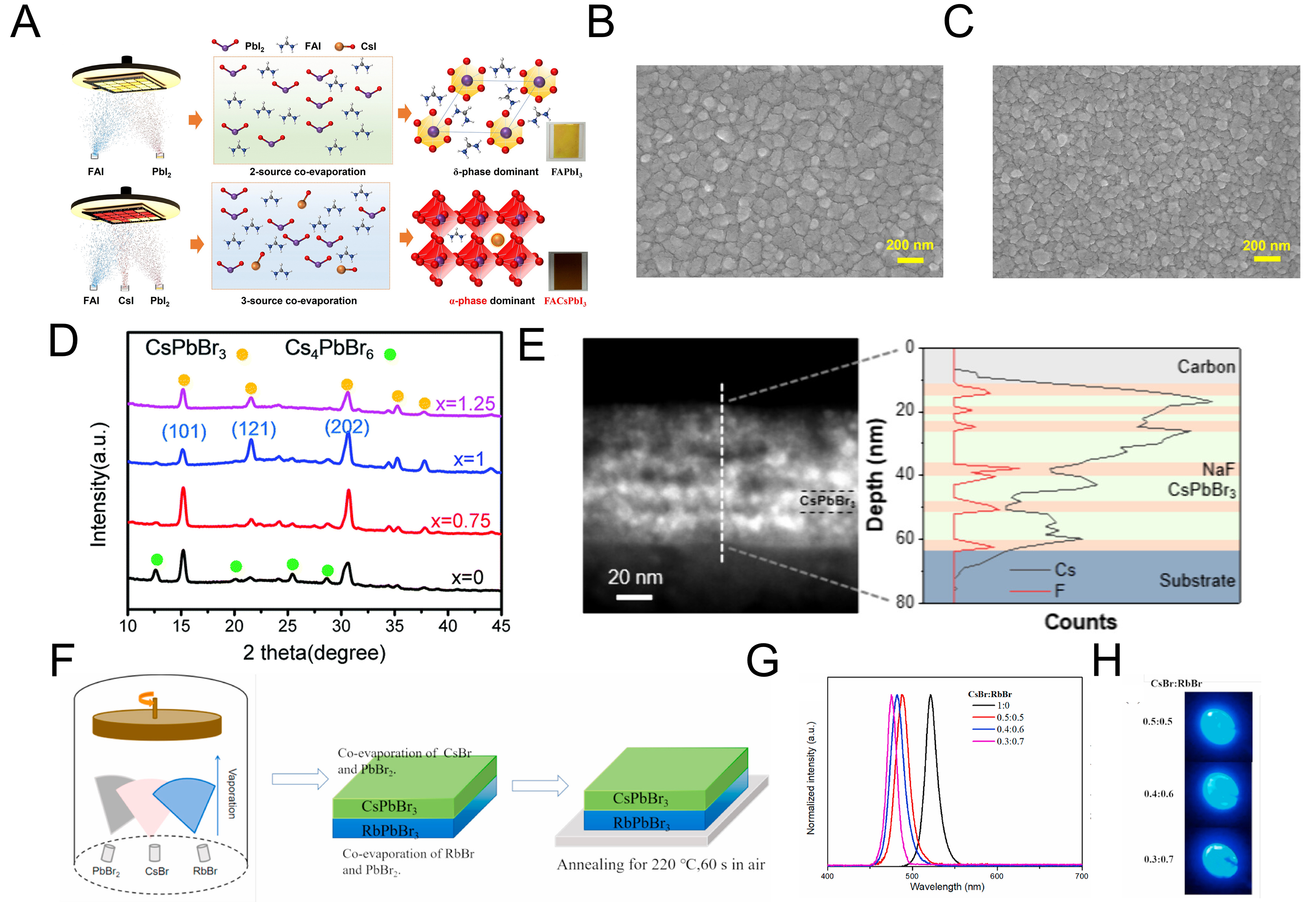
Figure 7. Variation of perovskite film properties with inorganic additives. (A) Illustration of phase transformation in FAPbI3 upon CsI addition; (B) SEM image of pristine FAPbI3 film; (C) SEM image after CsI incorporation[110]. Copyright 2025 Springer; (D) Cross-sectional HAADF-STEM image of alternating six-layer deposition of NaF and CsPbBr3 by vacuum evaporation (E) XRD patterns of CsPbBr3 depending on the presence of NaF interlayers[118]. Copyright 2025 American Chemical Society; (F) schematic illustration of sequential deposition of RbBr/PbBr2 followed by CsBr/PbBr2 and the corresponding film formation; (G) PL spectra as a function of RbBr/CsBr ratio, and (H) optical images under UV illumination[119]. Copyright 2025 Elsevier. FAPbI3: Formamidinium lead iodide; FA: formamidinium; SEM: scanning electron microscopy; HAADF-STEM: high-angle annular dark-field scanning transmission electron microscopy; XRD: X-ray diffraction; PL: photoluminescence; UV: ultraviolet.
A similar strategy has been applied in the fabrication of blue PeLEDs using CsPb(Cl/Br)3. In this case, dual-source TE employing CsCl and PbBr2 was compared with multi-source TE using CsCl, CsBr, and PbBr2[111]. The study revealed that employing two CsX sources led to the formation of Cs4Pb(Cl/Br)6, and that optimizing the ratio of CsPb(Cl/Br)3 to Cs4Pb(Cl/Br)6 yielded improved device performance.
Analogous to alkali-metal doping widely employed in perovskite quantum dots[39,112-114], recent studies have introduced inorganic alkali halides into TE to enhance device efficiency. The effect of the alkali metal strongly depends on its ionic radius: ions of suitable size can occupy the A-site, while ions that are too small or too large tend to segregate at the grain boundaries, thereby exerting different influences[115]. For example, incorporation of LiBr during deposition introduces Li+ and Br- ions, which help suppress bromide vacancies and lower the activation energy for ion diffusion, facilitating mass transport within the perovskite lattice[116]. Similarly, the introduction of NaBr together with CsBr and PbBr2 effectively suppresses the formation of Cs4PbBr6, a phase that hinders charge injection[117]. By characterizing XRD patterns of MHPs, films deposited with CsBr:PbBr2:NaBr ratios of 9-x:4:x exhibit a reduction in Cs4PbBr6 peaks for x ≥ 1, while maintaining the CsPbBr3 phase. At x = 1, the surface defect density of the films was also minimized.
TE further enables the construction of stacked structures that are difficult to realize in solution processing. For instance, alternating 1 nm NaF and 10 nm CsPbBr3 layers produced nanoscale grains with suppressed defect formation[118]. Owing to the small lattice mismatch between NaF and CsPbBr3, NaF serves as an effective defect passivator at the perovskite interface. Cross-sectional high-angle annular dark field scanning transmission electron microscopy (HAADF-STEM) images [Figure 7D] confirm the presence of six alternating layers. When CsPbBr3 films with thicknesses of 20 and 40 nm were alternately deposited with NaF, the XRD patterns [Figure 7E] revealed that the intensities of the (110) and (220) peaks decreased, while the (112) peak intensity increased. This indicates that the crystallographic orientation becomes more enhanced in the MHP regions closer to the NaF layer. Additional GABr treatment at the interface with the charge transport layer further reduced interfacial defects, leading to devices with an EQE of 7.21% and a luminance as high as 35,289 cd·m-2.
In another approach, Rb+ incorporation was investigated as an alternative to Cs+ for blue LED emission without the addition of chloride[119]. Dual-source TE of RbBr and PbBr2, as well as CsBr and PbBr2, was carried out [Figure 7F], and the resulting optical and electrical properties were studied as a function of Rb:Cs ratio. Because the ionic radius of Rb+ is smaller than that of Cs+, increasing Rb content induced a blue shift in the emission and enhanced the migration activation energy, thereby suppressing ion migration. The PL peak shift with increasing Rb fraction is shown in Figure 7G, while the EL images under applied bias for devices with different Rb ratios are displayed in Figure 7H.
Overall, the incorporation of inorganic additives during TE has served primarily to control defects, suppress undesired phase formation, and enhance crystallinity, leading to improved efficiency and stability, analogous to the role of organic additives. Nevertheless, unlike the well-established A-site or halide additives, systematic B-site doping via TE has not yet been explored. Furthermore, there have been no reports of simultaneous incorporation of multiple inorganic additives. These directions represent promising opportunities for further improving the performance of PeLEDs.
STRATEGIES FOR IMPROVING THE PERFORMANCE
To further enhance the performance and stability of TE-based PeLEDs, recent research has moved beyond process optimization and additive engineering to explore structural and material innovations. While deposition parameters such as precursor ratio, substrate temperature, and post-annealing conditions provide crucial control over film quality, these approaches alone cannot fully address the challenges of compositional uniformity, exciton management, and operational durability. In this context, several emerging strategies, ranging from advanced powder synthesis for single-source TE, to the adaptation of host-dopant architectures from organic LEDs, and the implementation of MQW structures, have attracted increasing attention. Together, these methods represent a paradigm shift from incremental optimization toward fundamental design principles that govern charge injection, exciton confinement, and radiative recombination. The following sections will highlight these strategies, emphasizing their potential to bridge the gap between laboratory demonstrations and practical display applications.
Synthesis of solid-state MHPs
A significant step toward scalable TE of MHP emitters lies in developing optimized precursors for single-source TEs. Conventional dual-source TE suffers from composition drift and limited stoichiometric control, leading to phase inhomogeneity and unstable emission[120]. Recent advances in powder synthesis, including ball-milling[121], solution methods[122], and other physical methods[123-126] [Figure 8A], have enabled uniform vapor transport and reproducible thin-film formation. Modifying precursor crystallinity, and compositional purity minimizes halide loss during evaporation, improving film stoichiometry, defect passivation, and spectral stability. These strategies not only facilitate reproducibility but also open the way toward finely tuned bandgap engineering and device-to-device uniformity in large-area displays.
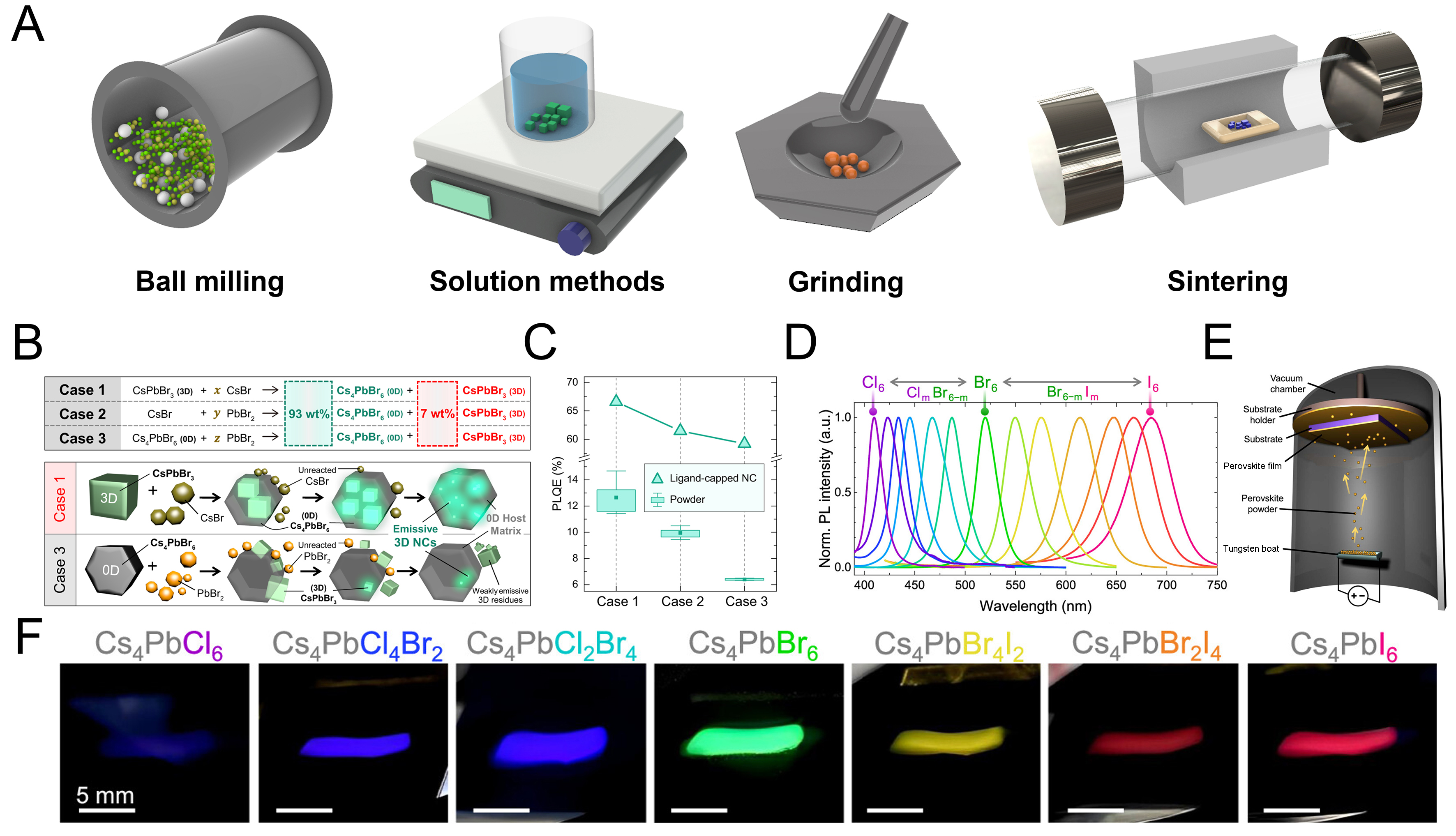
Figure 8. Solid-state synthesis of perovskites and powder preparation by ball milling. (A) Schematic illustration of various solid-state synthesis methods for perovskites; (B) Schematic mechanism of the formation of Cs4PbBr6 and CsPbBr3; (C) Comparison of PLQY values of three synthesized powders with those of perovskite nanocrystals prepared by the same method[130]. Copyright 2022 Nature; (D) PL spectra of Cs4PbX6 synthesized by ball milling with different halides; (E) Schematic illustration of the single-source deposition process; (F) Optical image of Cs4PbX6 films fabricated by single-source TE[131]. Copyright 2023 American Chemistry Society.
The most widely adopted method for synthesizing solid-state MHP powders is ball milling. Two common variants are wet ball milling, in which solution-phase precursors are mixed, and dry ball milling, which employs only solid precursors. Long-chain ligands such as oleic acid (OA) and oleylamine (OAm), conventionally used for quantum dot synthesis, were introduced during the milling process to prepare powders emitting in the sky-blue and green spectral ranges[127-129]. These ligands facilitate nanocrystal formation by widening the interparticle distance. More recently, high-energy dry ball milling has emerged as a robust strategy to produce powders with uniform particle size distributions[130].
Comparable to previous studies employing mixed CsPbBr3 and Cs4PbBr6 phases in both solution and TE, solid-state MHP synthesis also exhibited phase evolution and changes in optical properties as a function of milling time. Milling durations ranging from 20 min to 48 h revealed that the most prominent CsPbBr3 phase fraction was achieved after 180 min of processing, corresponding to the highest optical quality. To elucidate this transformation, the reaction pathway was analyzed [Figure 8B]. Three representative cases were proposed: (1) CsPbBr3 serving as the primary phase with excess CsBr attaching at the surface to yield Cs4PbBr6; (2) CsBr and PbBr2 combining in specific ratios to generate both Cs4PbBr6 and CsPbBr3; and (3) Cs4PbBr6 binding with PbBr2 to coexist with CsPbBr3. Across all scenarios, the optimal composition for photophysical performance corresponded to a Cs4PbBr6:CsPbBr3 ratio of 93:7 wt%, with Case 1 producing the most superior optical characteristics. As shown in Figure 8C, the optical properties were consistent with those reported for solution-processed perovskite nanocrystals, further validating the milling-based approach.
Dry ball milling has also been extended to the synthesis of Cs4PbBr6 powders (X = Cl, Br, I), enabling emission tunability from blue to red[131]. As illustrated in Figure 8D, varying the halide composition shifted the PL peak from 410 to 690 nm, with FWHM values spanning 17-60 nm closely resembling those of solution-synthesized perovskites. Moreover, these powders were successfully employed as single-source TE precursors: after placement in tungsten boats, they yielded high-quality thin films via TE [Figure 8E]. Interestingly, for iodine-containing powders, both α- and δ-CsPbI3 phases emerged, attributed to thermally induced phase transitions during deposition. This highlights the critical importance of minimizing deposition time to suppress thermal degradation and decomposition, particularly when employing ball-milled powders. The resulting thin films, when exposed to UV illumination, exhibited distinct emission images [Figure 8F]. This demonstrates that dry-milled powders are not only compositionally tunable but also directly compatible with TE workflows, underscoring their potential as scalable sources for high-quality thin films.
Solution-mediated synthesis routes for perovskite powders have also been reported. Here, long-chain ligands are typically removed by centrifugation or vacuum oven drying, enabling the recovery of solid-state nanocrystals in large quantities[132-134]. For microscale and larger powders, slow crystallization at low temperature from precursor solutions has been widely employed to yield single crystals with fewer defects[135-141]. For instance, CsPbBr3/Cs4PbBr6 composites were obtained by dissolving cesium acetate (CsAc) and PbBr2 in Dimethyl sulfoxide (DMSO), followed by HBr-assisted precipitation and DMSO washing[142]. The yield and PLQY strongly depended on the CsAc/PbBr2 ratio and washing solvent volume, reaching up to ~70% yield and 97% PLQY. As shown in Figure 9A, powders synthesized with a CsAc/PbBr2 ratio of 4 displayed bright luminescence under UV excitation. Corresponding XRD patterns indicated that ratios above 5 produced unidentified phases with CsBr peaks, whereas ratios below 4 predominantly yielded Cs4PbBr6 [Figure 9B]. Consistent with other sections, coexisting CsPbBr3 and Cs4PbBr6 phases enhanced emission efficiency by facilitating carrier transfer and surface defect passivation, while also improving stability under ambient exposure [Figure 9C].
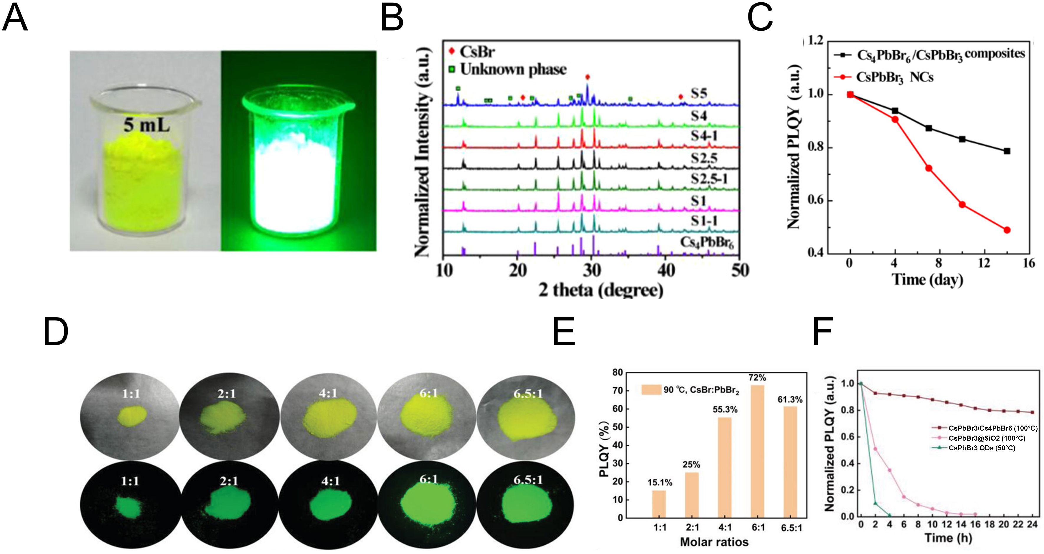
Figure 9. Data on solid-state perovskite synthesis using solution processing. (A) Optical and UV-illuminated images of powders synthesized with a 4:1 ratio of CsAc:PbBr2; (B) XRD patterns as a function of CsAc:PbBr2 ratio and the amount of DMSO used for washing; (C) PLQY stability test of solid-state CsPbBr3 and Cs4PbBr6 powders compared with CsPbBr3 nanocrystals upon air exposure[142]. Copyright 2018 American Chemistry Society; (D) Optical images of powders under UV and ambient light with CsBr:PbBr2 ratios varied from 1:1 to 6.5:1; (E) PLQY data as a function of CsBr:PbBr2 ratio; (F) Comparison of the stability of powders synthesized at high temperature with SiO2-coated materials and quantum dots[143]. Copyright 2021 John Wiley & Sons. PLQY: Photoluminescence quantum yield; PL: photoluminescence; TE: thermal evaporation.
An alternative approach involved mixing CsBr and PbBr2 with OA and OAm in Dimethylformamide (DMF)/DMSO solvents, followed by HBr addition, to form perovskite powders with nanometer-scale dimensions[143]. Unlike the CsAc-based method, no unidentified phases were detected even at CsBr/PbBr2 ratios as high as 6:1. As shown in Figure 9D, powders exhibited strong luminescence under UV excitation, and at a ratio of 6, the Cs4PbBr6:CsPbBr3 mixture achieved optimal defect passivation and the highest PLQY [Figure 9E]. Thermal stability, a prerequisite for TE, was further validated by comparing bare CsPbBr3 powders with SiO2-coated counterparts and perovskite quantum dots. As illustrated in Figure 9F, the powders exhibited excellent stability up to 100 °C. Nevertheless, given that vacuum deposition processes often require substantially higher thermal loads, the design of powders with enhanced high-temperature stability remains a critical challenge for future research.
Host-dopant system
The host-dopant system, well established in organic LEDs, offers new opportunities for PeLEDs. By embedding highly emissive perovskite nanocrystals or reduced-dimensional domains as dopants within wide-bandgap host matrices, concentration quenching can be suppressed, Auger recombination reduced, and exciton confinement enhanced. The host environment simultaneously controls charge transport pathways, facilitating balanced carrier injection while protecting the emissive domains from environmental degradation. Importantly, rational host selection - whether organic semiconductors with tailored frontier orbitals or insulating scaffolds with controlled polarity - enables tunable recombination dynamics and suppression of non-radiative decay, thereby bridging the performance gap between PeLEDs and organic LED structures. This cross-disciplinary perspective highlights the potential of host-dopant systems to accelerate the commercialization of PeLEDs.
In host-dopant systems, the host material is typically chosen to possess a wider bandgap than the dopant[144]. When a narrower bandgap dopant material is incorporated at concentrations of up to ~10%, spatially confined excitons and charge carriers, corresponding to the Cs4PbBr6-CsPbBr3 structure, promote radiative recombination, enhancing the PLQY. For example, the lead-free perovskite CsCu2I3 was synthesized via sintering and subsequently employed as a dopant in various organic host materials. As shown in Figure 10A, three different wide-bandgap organic hosts with distinct band alignments were investigated for their ability to improve device performance[145]. Among these, tri(m-pyridin-3-ylphenyl)benzene (TmPyPB) was found to be the most effective host because the CBM and VBM of CsCu2I3 align favorably within the highest occupied molecular orbital (HOMO) and lowest unoccupied molecular orbital (LUMO) of TmPyPB. This alignment enabled efficient exciton and carrier management within the perovskite, resulting in nearly a 20-fold increase in PLQY. Furthermore, as illustrated in Figure 10B, EL spectra revealed a single sharp emission peak without secondary features, confirming the success of this host-dopant strategy. The optimized devices achieved a high EQE of 7.4% along with operational stability exceeding 20 h.
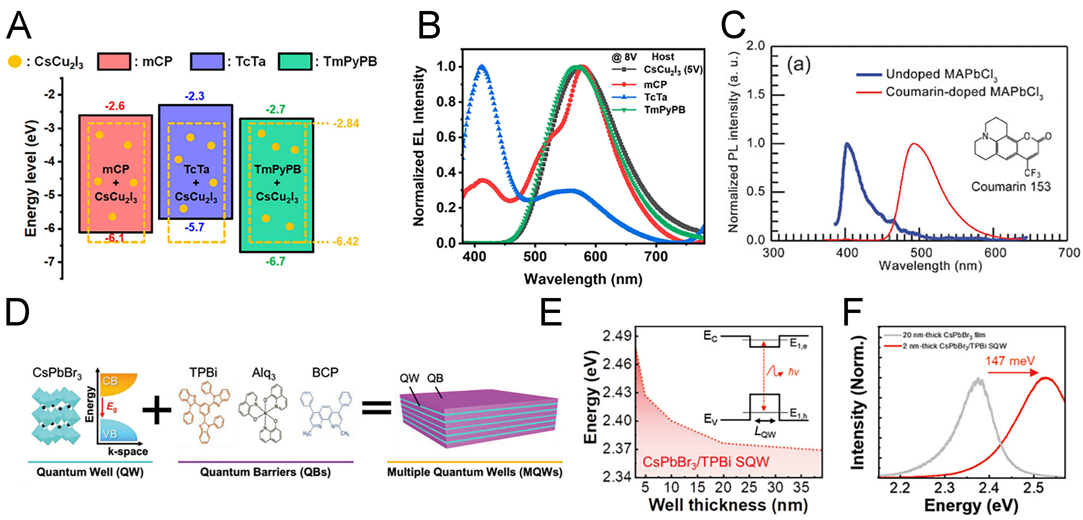
Figure 10. Characteristics of host-dopant systems and MQWs. (A) Energy alignment of three organic hosts with CsCu2I3; (B) PL spectra of perovskite-doped and undoped CsCu2I3 using three organic host materials compared with bulk CsCu2I3[145]. Copyright 2021 American Chemistry Society; (C) PL spectra of MAPbCl3 with and without Coumarin 153 doping[146]. Copyright 2018 John Wiley & Sons; (D) Schematic illustration of MQW structure formation using single-crystal CsPbBr3 and three organic materials; (E) Band gap variation as a function of TPBi thickness in single QW structures formed with TPBi and CsPbBr3; (F) Corresponding changes in PL peak position[148]. Copyright 2021 John Wiley & Sons. PL: Photoluminescence; MAPbCl3: methylammonium lead chloride; MA: methylammonium; MQW: multiple quantum well; QW: quantum well; TPBi: 2,2’,2’’-(1,3,5-benzinetriyl)-tris(1-phenyl-1H-benzimidazole).
Conversely, research has also explored the use of perovskites as hosts with organic dopants[146]. To this end, MAPbCl3 films were fabricated by dual-source vacuum deposition of MACl and PbCl2, yielding a wide-bandgap perovskite host. When doped with coumarin, the molecular frontier orbitals of coumarin resided within the HOMO-LUMO gap of MAPbCl3, facilitating efficient energy transfer. At 1% coumarin doping, the highest PL intensity was observed. As shown in Figure 10C, pristine MAPbCl3 exhibited a PL peak at ~400 nm, whereas coumarin doping induced a red-shifted, broadened emission peak in the green region. This spectral shift suggests absorption by the perovskite followed by energy transfer to the coumarin dopant. Compared with conventional organic hosts, MAPbCl₃-based devices demonstrated enhanced EQE, reduced turn-on voltage, and overall improved electrical performance.
One important set of challenges in host-dopant systems remains to be fully resolved. Although embedding MHPs in inorganic or organic host matrices can effectively suppress nonradiative recombination, excessive spatial isolation of the emissive domains can reduce percolation pathways and hinder charge transport, leading to increased driving voltages and reduced current efficiency at higher luminance. In addition, efficiency roll-off often arises from poor carrier balance at high brightness, where limited charge mobility in the host or insufficient charge injection into the dopant phase can cause exciton quenching or charge accumulation. From a processing standpoint, co-evaporation in TE-based fabrication presents practical difficulties in precisely controlling the individual deposition rates of host and dopant, especially for multi-component stacks and very low dopant concentrations, which can result in compositional drift and device-to-device variability. Addressing these related issues of transport, carrier balance, and process control will be crucial for translating host-dopant strategies into robust, scalable PeLEDs[147].
Multi-quantum well structure
Another powerful strategy involves MQW structures, wherein alternating layers of wide- and narrow-bandgap perovskites confine carriers and excitons within emissive wells. This engineered energy landscape reduces carrier diffusion losses, enhances radiative recombination rates, and enables efficient color purity tuning, such as a host-dopant system. MQWs further mitigate ion migration by providing structural barriers, thus improving operational stability. Advanced deposition protocols have demonstrated controllable well thickness and composition, unlocking improved EQE and operational lifetimes.
The formation of MQW structures requires the sequential TE of wide-bandgap organic barrier materials and perovskite layers. Since the optoelectronic properties strongly depend on the thickness of each layer, precise thickness control is critical. For this reason, single-source TE has been primarily employed as the deposition method. As shown in Figure 10D, single-crystalline CsPbBr3 was synthesized, ground into an evaporation source, and subsequently deposited together with organic barrier materials such as TPBi, tris-(8-hydroxyquinoline)aluminum (Alq3), and 2,9-dimethyl-4,7-diphenyl-1,10-phenanthroline (BCP) to construct multilayer MQW structures[148]. In the case of single-quantum well (QW) structures, the PL peak position was shifted depending on the thickness of the CsPbBr3 layer, while the extent of blue-shift varied with the type of organic barrier employed. The largest blue shift was observed in CsPbBr3/TPBi single-QWs [Figure 10E]. This behavior can be explained by the different band alignments: TPBi and Alq3 exhibit type-I band alignment with CsPbBr3, enabling both electrons and holes to transfer into the perovskite layer, whereas BCP exhibits type-II band alignment, driving electrons into the BCP layer. Due to its larger barrier height compared to Alq3 and BCP, TPBi induced nearly a twofold stronger blue shift, which is evident in the PL spectra [Figure 10F].
Optimization of such MQW structures has revealed that ultrathin CsPbBr3 layers combined with TPBi barriers enable the fabrication of blue-emitting perovskite materials without the need for chloride incorporation. Conversely, MQW structures with relatively thick CsPbBr3 layers exhibited a red shift in their PL spectra[149]. Compared with bulk CsPbBr3, all MQW configurations demonstrated superior optical properties owing to efficient exciton confinement and energy transfer. However, despite these promising results, the direct integration of MQW perovskite structures into operational LEDs has not yet been realized, underscoring the need for further research on device-level implementation.
APPLICATION OF EVAPORATED DEVICES
Recent reports have demonstrated direct integration with thin-film transistor (TFT) backplanes, enabling high-resolution, large-area, and flexible displays[150]. The advantages of TE, such as precise thickness control, pattern, and compatibility with established organic LED infrastructure, made this pathway particularly attractive for industrial adoption. Beyond displays, PeLEDs fabricated by TE have shown promise in optoelectronic integration, including photonic chips,
Ji et al. successfully fabricated a device comprising 64 pixels by combining MoS2-based TFTs characterized by fast response speed and high on/off ratio with single-source TE-based LEDs, as shown in Figure 11A[151]. They systematically investigated the phase transformation and properties of CsPbBr3 powders before and after TE, confirming uniform optical characteristics across a large-area 5 cm × 5 cm substrate with minimal deviation [Figure 11B]. Based on this, they demonstrated the driving of all 64 pixels in the integrated structure, where the controllable scan and data lines enabled pixel-addressable PeLED operation. The uniform EL of all pixels is clearly illustrated in Figure 11C.
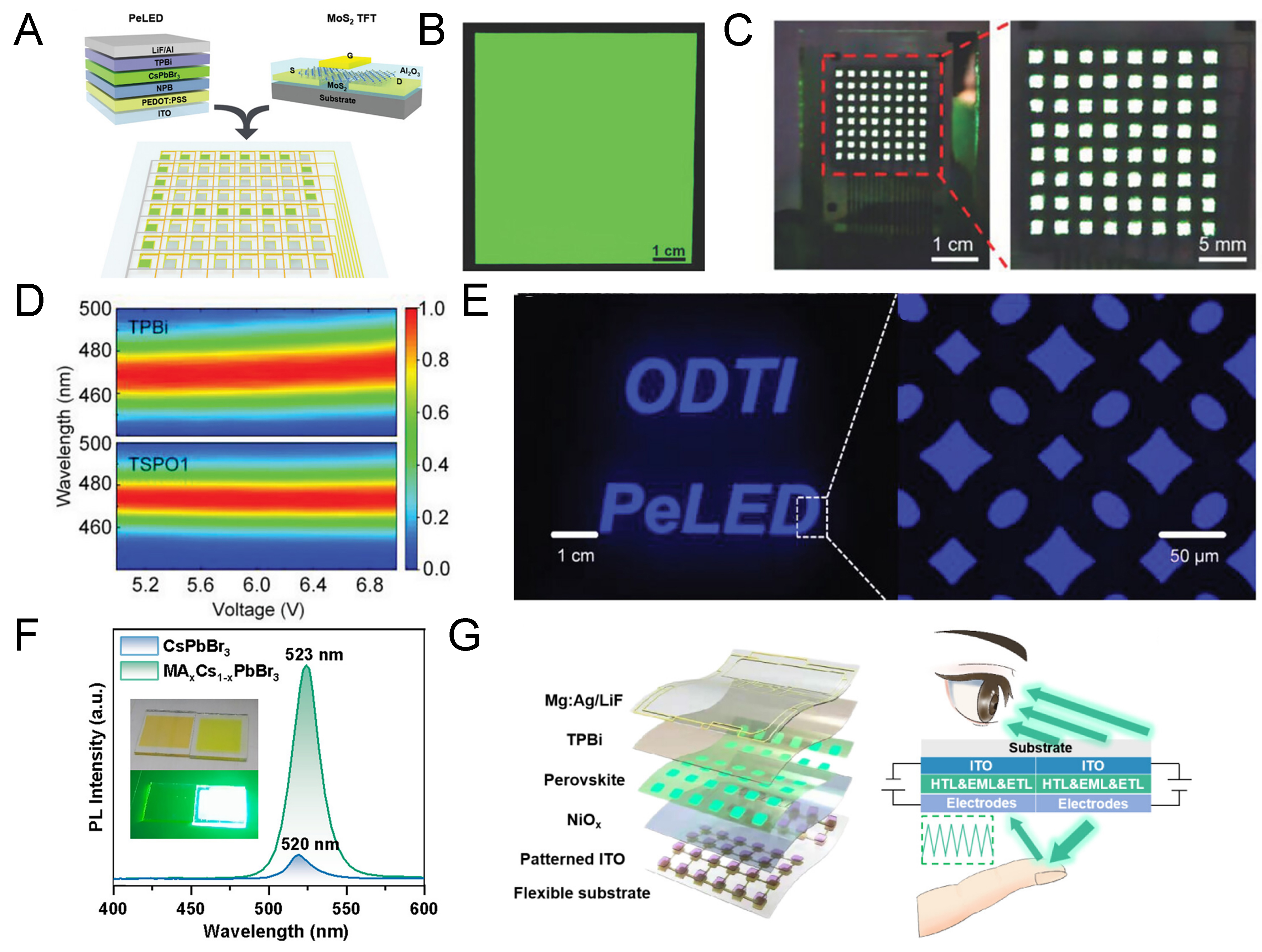
Figure 11. Images of applications fabricated by vacuum deposition. (A) Schematic illustration of integrating vacuum-deposited PeLEDs with MoS3-based TFTs; (B) Optical image of perovskite films deposited on a large-area substrate[151]. Copyright 2024 John Wiley & Sons; (C) Device image showing all pixels in the on-state; (D) Spectral stability of devices with two different electron transport layers as a function of voltage; (E) Optical image of a TSPO1-based top-emitting LED integrated with a TFT[153]. Copyright 2024 John Wiley & Sons; (F) PL spectra of CsPbBr3 with and without MABr incorporation; (G) Schematic illustration of LEDs capable of both top and bottom emission and their application in a heart-rate sensor[156]. Copyright 2024 American Chemistry Society. PeLED: Perovskite light-emitting diode; MoS2: molybdenum disulfide; TFT: thin-film transistor; TSPO1: 2-(4-tert-butylphenyl)-5-(4-biphenylyl)-1,3,4-oxadiazole; PL: photoluminescence; CsPbBr3: cesium lead bromide; MABr: methylammonium bromide.
In addition to green-emitting devices, active-matrix integration has also been investigated for blue and red PeLEDs[152]. For blue-emitting devices, enhanced crystal growth kinetics were achieved by introducing TPPO treatment, which controls the growth rate through P=O bonding, improving film quality. Furthermore, by applying Diphenyl[4-(triphenylsilyl)phenyl]phosphine oxide (TSPO1) instead of the commonly used TPBi electron transport layer, the devices exhibited a narrower FWHM and enhanced spectral stability [Figure 11D][153]. These improvements were attributed to the suppression of ion migration and mitigation of interfacial defects by TSPO1. Utilizing this structure, a top-emitting PeLED was integrated with TFTs, achieving active-matrix operation [Figure 11E]. In the case of red-emitting devices, the incorporation of 5-aminovaleric acid successfully suppressed Pb0 defects, thereby improving the film quality of FACsPb(Br/I)3 perovskites. This strategy enabled the fabrication of large-area and active-matrix red PeLEDs[154].
Beyond active-matrix displays, applications based on patterned perovskite films and flexible substrates have also been explored[155]. By incorporating MABr into CsPbBr3 films, charge injection balance was improved, and the formation energy of Br vacancies was increased, effectively suppressing defects. This was confirmed by the enhancement of PL intensity [Figure 11F][156]. Applying this improved film to LED, dual-mode devices capable of both top- and bottom-emission were fabricated. When integrated into flexible substrates, such devices demonstrated applicability as wearable photonic sensors, such as heart rate monitors. The structure and operating principles of the LED are illustrated in Figure 11G. Specifically, bottom emission enables detection of reflected light upon skin contact, which was effectively utilized for pulse sensing. The fabricated device showed comparable performance to commercial heart rate sensors under ambient and dark conditions, highlighting its potential for practical bio-integrated applications.
Overall, TE-based PeLEDs are particularly attractive for applications requiring large-area uniformity and high-resolution patterning. Their compatibility with diverse substrates and device structures further broadens their applicability, offering promising opportunities in next-generation displays, flexible electronics, and wearable optoelectronics. Table 1 summarizes the performance of all devices, spanning from additive engineering to their application. Additionally, to assess the progress in performance improvement of vacuum-deposited PeLEDs relative to solution-processed devices, we compared luminance and EQE as a function of wavelength [Figure 12]. In the green and red spectral regions, solution-processed PeLEDs generally exhibit superior performance[157-160]; however, in the blue region, both approaches show similarly low efficiencies, which can be attributed to the high defect density commonly encountered in blue-emitting perovskites[9,161-169]. Although a direct comparison of operational stability is complicated by differences in driving current density and initial luminance among the reported studies, it can still be observed that solution-processed PeLEDs tend to demonstrate overall improved stability compared with vacuum-deposited devices.
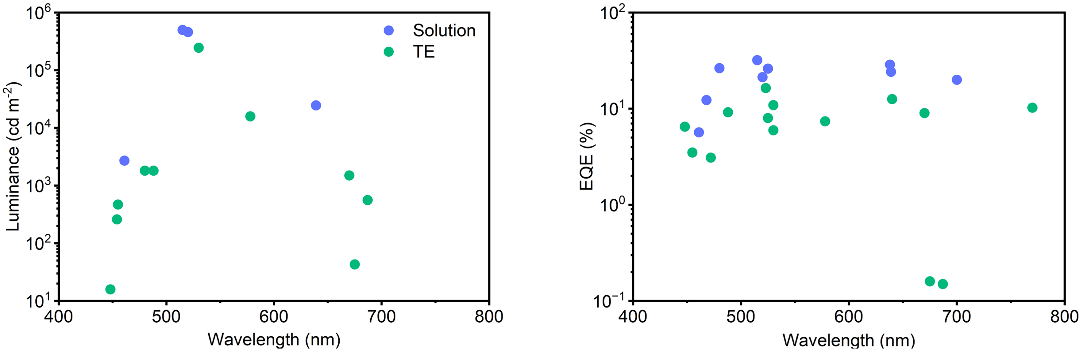
Figure 12. Graphs for comparing the electrical properties of solution-based PeLEDs and TE-based PeLEDs depending on wavelength. PeLED: Perovskite light-emitting diode; TE: top-emitting.
Summary of the detailed performance of vacuum-deposited PeLEDs
| Structure of LED | Process optimization and additive engineering | Luminance (cd·m-2) | EQE (%) | Ref. |
| ITO/PEDOT:PSS/Poly-TPD/CsPbBr3/TmPyPB/Liq/Al | Rate of TE (CsBr:PbBr2) | 5,765 | 1.55 | [54] |
| ITO/MoO3/TCTA/CsPbBr3/TPBi/LiF/Al | Rate of TE (CsBr:PbBr2) | 1,800 | 1.1 | [59] |
| ITO/PEDOTPSS/CsPbBr3:Cs4PbBr6/TPBi/LiF/Al | Rate of TE (CsBr:PbBr2) | 53,486 | 2.5 | [60] |
| ITO/m-PEDOT:PSS/CsPbBr3/TmPyPB/Liq/Al | Rate of TE (CsBr:PbBr2) | 1,607 | - | [63] |
| ITO/HAT-CN/TAPC/CsPbBr3/PO-T2T/Liq/Al | Substrate temperature (60 °C) | 17,350 | - | [66] |
| ITO/PEDOT:PSS/Poly-TPD/CsPbX3/TPBi/LiF/Al | Substrate temperature (100 °C) | 11,941 | 0.57 | [67] |
| ITO/NiOx/2PACz/CsPb(Cl/Br)3/TPBi/LiF/Al | Substrate temperature (-10 °C) | 1,640 | 7.2 | [69] |
| ITO/MoO3/TAPC/TCTA/CsSnBr3/TmPyPB/Li/Al | Substrate temperature (85 °C) | 43 | 0.16 | [68] |
| ITO/PVK/CsPbBr3/TPBi/LiF/Al | Post-annealing (90 °C) | 39,700 | 1.6 | [71] |
| Au/p-NiO/CsPbBr3/n-Si/Al | Post-annealing (240 °C) | 51,933 | 0.24 | [72] |
| Ag/N-Si/CsPbBr3:Cs4PbBr6/NiO/ITO | Post-annealing (300°C) | 957 | - | [73] |
| ITO/LiF/CsEuBr3/LiF/TPBi/LiF/Al | Post-annealing (200°C) | 5.2 | 6.5 | [74] |
| ITO/PEDOT:PSS/CsCu2I3/TPBi/LiF/Al | Modifying structure | 29.3 | 0.025 | [84] |
| ITO/HTL/CsPbBr3/TPBi/LiF/Al | Modifying structure | 9,442 | 3.26 | [86] |
| ITO/PEDOT:PSS/18-crown-6/CsPbBr3/TPBi/LiF/Al | Modifying structure | 15,520 | 1.02 | [87] |
| ITO/HAT-CN/TAPC/CzSi/GABr/CsPbBr3/GABr/PPT/3P-T2T/LiF/Al | Modifying structure | 75,300 | 21.1 | [89] |
| ITO/NiOx/PVK/CsPbBr3/TPBi//LiF/Al | Modifying structure | - | 8.6 | [76] |
| ITO/LiNiOx/CsPbBr3/TPBi/LiF/Al | Modifying structure | 11,133 | 1.24 | [88] |
| ITO/PEDOT:PSS/PEABr:MAPbBr3/TPBI/Liq/Al | Organic additive (quasi-2D) | 6,200 | 0.36 | [98] |
| ITO/TFB/PVK/Perovskite:PEABr/TPBi/LiF/Al | Organic additive (quasi-2D) | 7,400 | 6.5 | [99] |
| ITO/CuPc/BABr:Perovskite//TPBi/LiF/Ag | Organic additive (quasi-2D) | 8,400 | 5.3 | [100] |
| ITO/MoOx/MoOx:NPB/NPB/CsPbBr3:MABr/TPBi/LiF/Al | Organic additive (defect engineering) | 246,211 | 5.97 | [101] |
| ITO/m-PEDOT:PSS/CsPbBr3:DPEPO/ZADN/LiF?Al | Organic additive (defect engineering) | 35,083 | 16.91 | [102] |
| ITO/NiOx/2PACz/CsPb(Cl/Br)3:MFCl/TPBi/LiF/Al | Organic additive (defect engineering) | 1,820 | 9.2 | [106] |
| ITO/NiOx/PVK/PEACl:CsPb(Cl/Br)3/TPBI/LiF/Al | Organic additive (quasi-2D) | 1,325 | 6.09 | [107] |
| ITO/TFB/2-F-TPPO:CsPbBrI2/TPBi/LiF/Al | Organic additive (defect engineering) | - | 12.6 | [108] |
| ITO/PEDOT:PSS/TFB/FACsPbI3/TPBi/LiF/Al | Inorganic additive (defect engineering) | 2.64 W·Sr-1·m-2 | 10.25 | [110] |
| ITO/PEDOT:PSS/NaBr:CsPbBr3/TPBi/LiF/Al | Inorganic additive (defect engineering) | ~40,000 | 0.33 | [117] |
| ITO/PEDOT:PSS/GABr/NaF:CsPbBr3/GABr/TPBi/LiF/Al | Inorganic additive (defect engineering) | 35,289 | 7.21 | [118] |
| Ag/N-Si/RbBr:CsPbBr3/NiO/ITO | Inorganic additive (defect engineering) | 656.4 | 1.53 | [119] |
| ITO/PEDOT:PSS/TAPC/TcTA:CsCu2I3/CsCu2I3:TmPyPB/LiF/Al | Host-Dopant | 15,879 | 7.4 | [145] |
| ITO/PEDOT:PSS/NPB/Perovskite:Alq3/Alq3/TPBi/LiF/Al | Host-Dopant | 11,440 | 6.27 | [144] |
| ITO/MoOx/NPB/CsPbBr3:TPPO/TPBi/LiF/Al | Active-matrix | - | 16.4 | [150] |
| ITO/PEDOTPSS/NPB/CsPbBr3/TPBi/LiF/Al | Active-matrix | 5,136 | 2.12 | [151] |
| ITO/ZnO/Al2O3/Cs3CeI6/MCP/TAPC/TAPC:HAT-CN/HAT-CN/Al | Active-matrix | 470 | 3.5 | [152] |
| ITO/MoOx/NPB/TCTA/Perovskite:TPPO/TSPO1/LiF/Al | Active-matrix | - | 2.47 | [153] |
| ITO/2PACz/CsxFA1-xPbI3:5-AVA/TPBi/LiF/Al | Active-matrix | 1,524 | 7.27 | [154] |
CONCLUSION AND OUTLOOK
While TE-based PeLEDs have progressed significantly, several bottlenecks remain. Achieving long-term operational stability requires a deeper understanding of halide migration, interface reactions, and trap-assisted recombination under high current densities. Developing scalable precursor powders with high reproducibility, coupled with real-time in situ monitoring during evaporation, will be important for industrial deployment. The translation of host-dopant systems and MQW engineering into manufacturable processes will demand a careful balance between structural complexity and fabrication feasibility. Finally, integrating PeLEDs into active-matrix displays will require breakthroughs in pixel patterning, defect density reduction, and environmental encapsulation. Also, nonuniform halide distribution, depending on the source position in the chamber, hindered LED performance and reduced color purity, while the patterning mask caused shadow effects on the emitting layer[165,166]. The red and blue PeLEDs fabricated using TE are expected to face challenges in performance improvement when applying the strategies employed in this work. TE offers clear advantages for commercialization, such as compatibility with large-area fabrication and precise patterning; however, it also suffers from several drawbacks. In multiple-TE configurations, cross-contamination between sources can reduce the purity of the deposited materials, and in the case of iodine-containing perovskites used as active layers in solar cells and red PeLEDs, iodine species have been detected in adjacent organic layers and metal electrodes, indicating various forms of process-induced contamination[167,168]. Addressing these processing-related issues, alongside improvements in efficiency and operational stability, will be essential if TE-based methods are to genuinely replace solution processing in perovskite device fabrication. With continued interdisciplinary advances spanning perovskite chemistry, thin-film engineering, and device physics, vacuum-deposited PeLEDs have the potential to rival or even surpass organic LEDs in next-generation display and optoelectronic technologies.
DECLARATIONS
Authors’ contributions
Proposed the topic of this review: Kim, SY.
Prepared the manuscript: Seol, MJ.
Data curation: Jeong, J.
Availability of data and materials
Not applicable.
Financial support and sponsorship
This work was supported by the National Research Foundation (NRF) of Korea (Grant number RS-2025-00558945).
Conflicts of interest
Kim, SY. is an Associated Editor of the journal Energy Materials and was not involved in any part of the editorial process, including reviewer selection, manuscript handling, or decision-making. The other authors declared that there are no conflicts of interest.
Ethical approval and consent to participate
Not applicable.
Consent for publication
Not applicable.
Copyright
© The Author(s) 2026.
REFERENCES
1. Liu, S.; Li, J.; Xiao, W.; et al. Buried interface molecular hybrid for inverted perovskite solar cells. Nature 2024, 632, 536-42.
2. Liang, Z.; Zhang, Y.; Xu, H.; et al. Homogenizing out-of-plane cation composition in perovskite solar cells. Nature 2023, 624, 557-63.
3. Jang, W. J.; Kim, E. H.; Cho, J. H.; Lee, D.; Kim, S. Y. Elucidating the role of alkali metal carbonates in impact on oxygen vacancies for efficient and stable perovskite solar cells. Adv. Sci. 2024, 11, e2406657.
4. Kang, S. B.; Patil, P.; Yoon, G. W.; Han, G. S.; Jung, H. S.; Kim, D. H. Study of interface engineering on perovskite-based indoor photovoltaics for powering Internet-of-Things. Chem. Eng. J. 2024, 502, 157973.
5. Kim, D.; Lee, S.; Kim, G. M.; Oh, S. Y. Physical effects of 2PACz layers as hole-transport material on the performance of perovskite solar cell. Electron. Mater. Lett. 2023, 19, 510-7.
6. Ali, S.; Javed, S.; Akram, M. A.; et al. Investigating the electrical and optical properties of nickle and strontium co-doped CsPbBr3 nanocrystals: potential absorber material for perovskite solar cells. Trans. Electr. Electron. Mater. 2024, 25, 422-33.
7. Fakharuddin, A.; Gangishetty, M. K.; Abdi-jalebi, M.; et al. Perovskite light-emitting diodes. Nat. Electron. 2022, 5, 203-16.
8. Chen, W.; Huang, Z.; Yao, H.; et al. Highly bright and stable single-crystal perovskite light-emitting diodes. Nat. Photon. 2023, 17, 401-7.
9. Jiang, J.; Shi, M.; Xia, Z.; et al. Efficient pure-red perovskite light-emitting diodes with strong passivation via ultrasmall-sized molecules. Science. Advances. 2024, 10, eadn5683.
10. Shin, G.; Yun, D.; Ha, Y.; et al. Enhancing performance of perovskite nanocrystal light-emitting diodes with perfluorinated ionomer and PEDOT:PSS. Trans. Electr. Electron. Mater. 2024, 25, 40-7.
11. Shinde, P. V.; Patra, A.; Rout, C. S. A review on the sensing mechanisms and recent developments on metal halide-based perovskite gas sensors. J. Mater. Chem. C. 2022, 10, 10196-223.
12. Hou, Y.; Li, J.; Yoon, J.; et al. Retina-inspired narrowband perovskite sensor array for panchromatic imaging. Sci. Adv. 2023, 9, eade2338.
13. Park, J.; Ahn, J.; Jung, B. K.; et al. Reusable gasochromic gas sensor with enhanced selectivity for acidic gases via surface-engineered all-inorganic perovskite nanocrystals. Chem. Eng. J. 2024, 498, 155420.
14. Liu, A.; Zhu, H.; Bai, S.; et al. High-performance metal halide perovskite transistors. Nat. Electron. 2023, 6, 559-71.
15. Kim, S. J.; Im, I. H.; Baek, J. H.; et al. Linearly programmable two-dimensional halide perovskite memristor arrays for neuromorphic computing. Nat. Nanotechnol. 2025, 20, 83-92.
16. Nketia-yawson, V.; Nketia-yawson, B.; Woong, Jo. J. High-mobility electrolyte-gated perovskite transistors on flexible plastic substrate via interface and composition engineering. Appl. Surf. Sci. 2023, 623, 156984.
17. Pathak, A. K.; Mukherjee, S.; Batabyal, S. K. 2D layered (CH3NH3)3Sb2ClxI9-x lead-free perovskite for weak light detection. Electron. Mater. Lett. 2024, 20, 425-31.
18. Seo, H.; Park, T.; Ali, A.; et al. Quantum dots and perovskites-based physically unclonable functions for binary and ternary keys via optical-to-electrical conversion. Adv. Funct. Mater. 2025, 35, 2507395.
19. Bhaumik, S.; Ray, S.; Batabyal, S. K. Recent advances of lead-free metal halide perovskite single crystals and nanocrystals: synthesis, crystal structure, optical properties, and their diverse applications. Mater. Today. Chem. 2020, 18, 100363.
20. Tan, Z. K.; Moghaddam, R. S.; Lai, M. L.; et al. Bright light-emitting diodes based on organometal halide perovskite. Nat. Nanotechnol. 2014, 9, 687-92.
21. Peng, C.; Yao, H.; Ali, O.; et al. Weakly space-confined all-inorganic perovskites for light-emitting diodes. Nature 2025, 643, 96-103.
22. Kim, J. S.; Heo, J. M.; Park, G. S.; et al. Ultra-bright, efficient and stable perovskite light-emitting diodes. Nature 2022, 611, 688-94.
23. Gao, Y.; Li, H.; Dai, X.; et al. Microsecond-response perovskite light-emitting diodes for active-matrix displays. Nat. Electron. 2024, 7, 487-96.
24. Yu, Y.; Wang, B. F.; Shen, Y.; et al. Efficient blue perovskite LEDs via bottom-up charge manipulation for solution-processed active-matrix displays. Adv. Mater. 2025, 37, e2503234.
25. Chen, Y.; Yang, X.; Fan, X.; et al. Electrohydrodynamic inkjet printing of three-dimensional perovskite nanocrystal arrays for full-color micro-LED displays. ACS. Appl. Mater. Interfaces. 2024, 16, 24908-19.
26. Mahyoub, S. A.; Farid, A.; Azeem, M. Z.; Fadhil, D. A. A.; Qaraah, F. A.; Drmosh, Q. A. Physical vapor deposition techniques for CO2 electroreduction: a review. Small. Struct. 2025, 6, 2400501.
27. Umar, A.; Hahn, Y. B. Aligned hexagonal coaxial-shaped ZnO nanocolumns on steel alloy by thermal evaporation. Appl. Phys. Lett. 2006, 88, 173120.
28. Wang, H.; Li, J.; Huang, M.; et al. Single-atom alloys prepared by two-step thermal evaporation. Nano. Res. 2024, 17, 2808-13.
29. Lee, G. Branched MgO nanowires synthesized by thermal evaporation method in air at atmospheric pressure. Korean. J. Met. Mater. 2023, 61, 444-8.
30. Lee, G. Effect of oxygen concentration on the growth and cathodoluminescence properties of MgO nanowires. Korean. J. Met. Mater. 2023, 61, 509-13.
31. Kim, S. K.; Kim, K.; Park, H.; et al. Patternization of cathode metal using low surface energy organic molecules in OLED thermal evaporation process. J. Ind. Eng. Chem. 2022, 114, 213-20.
32. Jung, S. W.; Kim, K.; Park, H.; et al. Patternable semi-transparent cathode using thermal evaporation for OLED display applications. Adv. Elect. Mater. 2021, 7, 2001101.
33. Chen, W.; Zhang, J.; Xu, G.; et al. A semitransparent inorganic perovskite film for overcoming ultraviolet light instability of organic solar cells and achieving 14.03% efficiency. Adv. Mater. 2018, 30, e1800855.
34. Yeh, K. C.; Chan, C. H. High brightness and low operating voltage CsPbBr3 perovskite LEDs by single-source vapor deposition. Sci. Rep. 2024, 14, 3351.
35. Zhang, C.; Chen, J.; Kong, L.; et al. Core/shell metal halide perovskite nanocrystals for optoelectronic applications. Adv. Funct. Mater. 2021, 31, 2100438.
36. Das Adhikari, S.; Gualdrón Reyes, A. F.; Paul, S.; et al. Impact of core-shell perovskite nanocrystals for LED applications: successes, challenges, and prospects. Chem. Sci. 2023, 14, 8984-99.
37. Park, M.; Park, J.; Lee, J.; et al. Efficient perovskite light‐emitting diodes using polycrystalline core-shell-mimicked nanograins. Adv. Funct. Mater. 2019, 29, 1902017.
38. Hou, S.; Gangishetty, M. K.; Quan, Q.; Congreve, D. N. Efficient blue and white perovskite light-emitting diodes via manganese doping. Joule 2018, 2, 2421-33.
39. Shi, Y.; Xi, J.; Lei, T.; et al. Rubidium doping for enhanced performance of highly efficient formamidinium-based perovskite light-emitting diodes. ACS. Appl. Mater. Interfaces. 2018, 10, 9849-57.
40. Yang, D.; Huo, D. Cation doping and strain engineering of CsPbBr3-based perovskite light emitting diodes. J. Mater. Chem. C. 2020, 8, 6640-53.
41. Wang, R.; Zhao, J.; Ma, J.; et al. Yttrium cation doping and phenylphosphonic acid passivation for pure-red perovskite light-emitting diodes. ACS. Energy. Lett. 2024, 9, 4699-707.
42. Chu, Z.; Zhang, W.; Jiang, J.; et al. Blue perovskite light-emitting diodes using multifunctional small molecule dopants. Adv. Mater. 2025, 37, e2409718.
43. Zhang, L.; Sun, C.; He, T.; et al. High-performance quasi-2D perovskite light-emitting diodes: from materials to devices. Light. Sci. Appl. 2021, 10, 61.
44. Sun, C.; Jiang, Y.; Cui, M.; et al. High-performance large-area quasi-2D perovskite light-emitting diodes. Nat. Commun. 2021, 12, 2207.
45. Zhang, F.; Cai, B.; Song, J.; Han, B.; Zhang, B.; Zeng, H. Efficient blue perovskite light-emitting diodes boosted by 2D/3D energy cascade channels. Adv. Funct. Mater. 2020, 30, 2001732.
46. Jiang, N.; Wang, Z.; Zheng, Y.; et al. 2D/3D heterojunction perovskite light-emitting diodes with tunable ultrapure blue emissions. Nano. Energy. 2022, 97, 107181.
47. He, Z.; Peng, C.; Guo, R.; et al. 2D/3D perovskite heterojunctions: composition and application in light-emitting diodes. Chem. Eng. J. 2025, 505, 159894.
48. Kuang, C.; Hu, Z.; Yuan, Z.; et al. Critical role of additive-induced molecular interaction on the operational stability of perovskite light-emitting diodes. Joule 2021, 5, 618-30.
49. Liu, Y.; Ono, L. K.; Qi, Y. Organic additive engineering toward efficient perovskite light‐emitting diodes. InfoMat 2020, 2, 1095-108.
50. Liu, Z.; Qiu, W.; Peng, X.; et al. Perovskite light-emitting diodes with EQE exceeding 28% through a synergetic dual-additive strategy for defect passivation and nanostructure regulation. Adv. Mater. 2021, 33, e2103268.
51. Islam, A.; Saeed Khan, R. A.; Khalid, A.; et al. Zwitterions: an innovative class of additive materials for perovskite light-emitting diodes. Mater. Today. Energy. 2025, 47, 101752.
52. Zou, S.; Fan, K.; Liu, Z.; et al. Additive-stabilized emission centers for blue perovskite light-emitting diodes. ACS. Appl. Mater. Interfaces. 2023, 15, 26778-86.
53. Liu, M.; Johnston, M. B.; Snaith, H. J. Efficient planar heterojunction perovskite solar cells by vapour deposition. Nature 2013, 501, 395-8.
54. Hu, Y.; Wang, Q.; Shi, Y.; et al. Vacuum-evaporated all-inorganic cesium lead bromine perovskites for high-performance light-emitting diodes. J. Mater. Chem. C. 2017, 5, 8144-9.
55. Mariano, F.; Listorti, A.; Rizzo, A.; Colella, S.; Gigli, G.; Mazzeo, M. Thermally evaporated hybrid perovskite for hetero-structured green light-emitting diodes. Appl. Phys. Lett. 2017, 111, 163301.
56. Liu, X.; Tan, X.; Liu, Z.; et al. Sequentially vacuum evaporated high-quality CsPbBr3 films for efficient carbon-based planar heterojunction perovskite solar cells. J. Power. Sources. 2019, 443, 227269.
57. Lee, W.; Lee, J.; Lee, H. D.; et al. Controllable deposition of organic metal halide perovskite films with wafer-scale uniformity by single source flash evaporation. Sci. Rep. 2020, 10, 18781.
58. Cho, H.; Jeong, S. H.; Park, M. H.; et al. Overcoming the electroluminescence efficiency limitations of perovskite light-emitting diodes. Science 2015, 350, 1222-5.
59. Xie, S.; Osherov, A.; Bulović, V. All-vacuum-deposited inorganic cesium lead halide perovskite light-emitting diodes. APL. Materials. 2020, 8, 051113.
60. Lian, X.; Wang, X.; Ling, Y.; et al. Light emitting diodes based on inorganic composite halide perovskites. Adv. Funct. Mater. 2019, 29, 1807345.
61. Otalora, C.; Botero, M. A.; Mantilla, M. A.; Petit, J. F.; Ospina, R.; Gordillo, G. Hybrid perovskite films deposited by thermal evaporation from a single source. J. Mater. Sci. Mater. Electron. 2021, 32, 12151-63.
62. Kim, S. J.; Byun, J.; Jeon, T.; Jin, H. M.; Hong, H. R.; Kim, S. O. Perovskite light-emitting diodes via laser crystallization: systematic investigation on grain size effects for device performance. ACS. Appl. Mater. Interfaces. 2018, 10, 2490-5.
63. Shin, M.; Lee, H. S.; Sim, Y. C.; Cho, Y. H.; Cheol Choi, K.; Shin, B. Modulation of growth kinetics of vacuum-deposited CsPbBr3 films for efficient light-emitting diodes. ACS. Appl. Mater. Interfaces. 2020, 12, 1944-52.
64. Rigi VJ, Jayaraj MK, Saji KJ. Effect of substrate and substrate temperature on the deposition of MoS2 by radio frequency magnetron sputtering. J. Vac. Sci. Technol. A. 2022, 40, 032201.
65. Gil-Escrig, L.; Nespoli, J.; Elhorst, F. D.; et al. Tuning substrate temperature for enhanced vacuum-deposited wide-bandgap perovskite solar cells: insights from morphology, charge transport, and drift-diffusion simulations. EES. Solar. 2025, 1, 391-403.
66. Chen, C.; Han, T. H.; Tan, S.; et al. Efficient flexible inorganic perovskite light-emitting diodes fabricated with CsPbBr3 emitters prepared via low-temperature in situ dynamic thermal crystallization. Nano. Lett. 2020, 20, 4673-80.
67. Han, B.; Shan, Q.; Zhang, F.; Song, J.; Zeng, H. Giant efficiency and color purity enhancement in multicolor inorganic perovskite light-emitting diodes via heating-assisted vacuum deposition. J. Semicond. 2020, 41, 052205.
68. Mu, H.; Hu, F.; Wang, R.; Jia, J.; Shuang, Xiao. Effects of in-situ annealing on the electroluminescence performance of the Sn-based perovskite light-emitting diodes prepared by thermal evaporation. J. Lumin. 2020, 226, 117493.
69. Peng, C.; He, Z.; Guo, R.; et al. The synergy of pre-frozen substrates and post-annealing for high-efficiency co-evaporated blue perovskite LEDs. Chem. Eng. J. 2024, 493, 152579.
70. Yuan, F.; Xi, J.; Dong, H.; et al. All‐inorganic hetero‐structured cesium tin halide perovskite light‐emitting diodes with current density over 900 A·cm-2 and its amplified spontaneous emission behaviors. Phys. Rapid. Res. Lett. 2018, 12, 1800090.
71. Huang, J.; Yao, H.; You, F.; et al. Effects of post-annealing on the property of CsPbBr3 films and the performance of relevant light-emitting diodes. J. Lumin. 2024, 275, 120771.
72. Xiang, G.; Zhou, Y.; Peng, W.; et al. Vacuum-deposited perovskite CsPbBr3 thin-films for temperature-stable Si based pure-green all-inorganic light-emitting diodes. Ceram. Int. 2023, 49, 21624-33.
73. Bai, T.; Wang, S.; Zhang, K.; Chu, C.; Sun, Y.; Yi, L. High stability and strong luminescence CsPbBr3-Cs4PbBr6 thin films for all-inorganic perovskite light-emitting diodes. RSC. Adv. 2023, 13, 24413-22.
74. Luo, J.; Yang, L.; Tan, Z.; et al. Efficient blue light emitting diodes based on europium halide perovskites. Adv. Mater. 2021, 33, e2101903.
75. Qiu, C.; Dumont, A.; Li, P.; Lu, Z. Thermally stable charge transport materials for vapor-phase fabrication of perovskite devices. Adv. Photonics. Res. 2021, 2, 2000140.
76. Peng, C.; He, Z.; Guo, R.; et al. The synergy of the buried interface surface energy and temperature for thermal evaporated perovskite light-emitting diodes. ACS. Appl. Mater. Interfaces. 2023, 15, 15768-74.
77. Li, J.; Yang, L.; Guo, Q.; et al. All-vacuum fabrication of yellow perovskite light-emitting diodes. Sci. Bull. 2022, 67, 178-85.
78. Kim, N.; Shin, M.; Jun, S.; et al. Highly efficient vacuum-evaporated CsPbBr3 perovskite light-emitting diodes with an electrical conductivity enhanced polymer-assisted passivation layer. ACS. Appl. Mater. Interfaces. 2021, 13, 37323-30.
79. Xu, L.; Zhou, L.; Yan, M.; Luo, G.; Yang, D.; Fang, Y. High-brightness thermally evaporated perovskite light-emitting diodes via dual-interface engineering. Opt. Mater. 2024, 150, 115223.
80. Song, L.; Huang, L.; Liu, Y.; et al. Efficient thermally evaporated perovskite light-emitting devices via a bilateral interface engineering strategy. J. Phys. Chem. Lett. 2021, 12, 6165-73.
81. Lee, S.; Woo, M. Y.; Kim, C.; et al. Buried interface modulation via PEDOT:PSS ionic exchange for the Sn-Pb mixed perovskite based solar cells. Chem. Eng. J. 2024, 479, 147587.
82. Kwack, H.; Kim, M.; Cho, Y.; Kim, T.; Myoung, J.; Shim, W. Thickness controlled CsPbBr3 nanocrystal films for high efficiency (6% EQE) perovskite LEDs. J. Korean. Ceram. Soc. 2025, 62, 1023-9.
83. Zhao, L.; Lee, K. M.; Roh, K.; Khan, S. U. Z.; Rand, B. P. Improved outcoupling efficiency and stability of perovskite light-emitting diodes using thin emitting layers. Adv. Mater. 2019, 31, e1805836.
84. Gu, Y.; Yao, X.; Long, M.; Geng, H.; Hu, M. Ultra-broadband light-emitting diodes from co-evaporated lead-free CsCu2I3. Mater. Lett. 2022, 323, 132607.
85. Jia, K.; Song, L.; Hu, Y.; et al. Improved performance for thermally evaporated perovskite light-emitting devices via defect passivation and carrier regulation. ACS. Appl. Mater. Interfaces. 2020, 12, 15928-33.
86. Li, J.; Du, P.; Li, S.; et al. High-throughput combinatorial optimizations of perovskite light-emitting diodes based on all-vacuum deposition. Adv. Funct. Mater. 2019, 29, 1903607.
87. Zhao, L.; Zhang, Y.; Sun, K.; et al. Crown-ether modified thermally evaporated perovskite light-emitting devices with increased operational stability. J. Lumin. 2022, 252, 119317.
88. Vo, V. K.; Bae, S. H.; Dang, T. H. T.; et al. Tetraoctylammonium bromide interlayer between NiLiOx and perovskite for light-emitting diodes. ACS. Appl. Mater. Interfaces. 2024, 16, 64210-21.
89. Hsieh, C. A.; Tan, G. H.; Chuang, Y. T.; et al. Vacuum-deposited inorganic perovskite light-emitting diodes with external quantum efficiency exceeding 10% via composition and crystallinity manipulation of emission layer under high vacuum. Adv. Sci. 2023, 10, e2206076.
90. Gao, Y.; Liu, Y.; Zhang, F.; et al. High-performance perovskite light-emitting diodes enabled by passivating defect and constructing dual energy-transfer pathway through functional perovskite nanocrystals. Adv. Mater. 2022, 34, e2207445.
91. Dong, C.; Chen, G.; Wang, S.; Yu, Z.; Ke, W.; Fang, G. High-performance green light-emitting-diode enabled by simultaneous phase engineering and crystallization regulation. Adv. Funct. Mater. 2025, 35, 2502662.
92. Warby, J. H.; Wenger, B.; Ramadan, A. J.; et al. Revealing factors influencing the operational stability of perovskite light-emitting diodes. ACS. Nano. 2020, 14, 8855-65.
93. Xiong, W.; Zou, C.; Tang, W.; et al. Efficient and bright blue perovskite LEDs enabled by a carbazole-phosphonic acid interface. ACS. Energy. Lett. 2023, 8, 2897-903.
94. Kirsch, C.; Naujoks, T.; Haizmann, P.; et al. Zwitterionic carbazole ligands enhance the stability and performance of perovskite nanocrystals in light-emitting diodes. ACS. Appl. Mater. Interfaces. 2023, 15, 32744-52.
95. Lai, Y.; Chen, C.; Yu, M.; et al. Dual functionality of carbazole-based phosphonic acid molecular additives realizes efficient hole transport layer-free perovskite light-emitting diodes. Chem. Eng. J. 2025, 504, 158876.
96. Kim, J. S.; Lee, H. D.; Jung, J. H.; et al. Kinetically-controlled intermediate-direct-pinning for homogeneous energy landscapes in quasi-two-dimensional perovskites for efficient and narrow blue emission. Nat. Commun. 2025, 16, 9590.
97. Yang, X.; Zhang, X.; Deng, J.; et al. Efficient green light-emitting diodes based on quasi-two-dimensional composition and phase engineered perovskite with surface passivation. Nat. Commun. 2018, 9, 570.
98. Chiang, K. M.; Hsu, B. W.; Chang, Y. A.; Yang, L.; Tsai, W. L.; Lin, H. W. Vacuum-deposited organometallic halide perovskite light-emitting devices. ACS. Appl. Mater. Interfaces. 2017, 9, 40516-22.
99. Wang, L.; Li, J.; Du, P.; et al. Effect of post-annealing on thermally evaporated reduced-dimensional perovskite LEDs. Appl. Phys. Lett. 2022, 120, 081107.
100. Fu, Y.; Zhang, Q.; Zhang, D.; et al. Scalable all-evaporation fabrication of efficient light-emitting diodes with hybrid 2D-3D perovskite nanostructures. Adv. Funct. Mater. 2020, 30, 2002913.
101. Meng, N.; Li, Y.; Shi, X.; et al. Fully thermal-evaporated perovskite light-emitting diodes with brightness exceeding 240 000 nits. Adv. Funct. Mater. 2025, 35, e10484.
102. Lee, M. H.; Kim, J.; Han, J.; et al. Fabrication of conductive perovskite-additive networks via sequential vacuum deposition for perovskite light-emitting diodes. ACS. Energy. Lett. 2025, 10, 2898-905.
103. Li, M.; Zhao, Y.; Qin, X.; et al. Conductive phosphine oxide passivator enables efficient perovskite light-emitting diodes. Nano. Lett. 2022, 22, 2490-6.
104. Zhao, C.; Wu, W.; Zhan, H.; et al. Phosphonate/phosphine oxide dyad additive for efficient perovskite light-emitting diodes. Angew. Chem. Int. Ed. Engl. 2022, 61, e202117374.
105. Lin, K.; Xing, J.; Quan, L. N.; et al. Perovskite light-emitting diodes with external quantum efficiency exceeding 20 per cent. Nature 2018, 562, 245-8.
106. Peng, C.; Chen, B.; Liu, X.; et al. High-performance thermally evaporated blue perovskite light-emitting diodes enabled by post-evaporation passivation. Chem. Eng. J. 2024, 499, 155955.
107. Sun, L.; He, X.; He, Z.; et al. Improved vacuum-evaporated blue perovskite light-emitting diodes with phenethylammonium chloride and guanidinium bromide synergistic post-processing modification. Front. Optoelectron. 2025, 18, 5.
108. Liu, N.; Liu, Z.; Huang, Y.; et al. Fluorine-modified passivator for efficient vacuum-deposited pure-red perovskite light-emitting diodes. Light. Sci. Appl. 2025, 14, 118.
109. Dong, J.; Zhao, B.; Ji, H.; et al. Multivalent-effect immobilization of reduced-dimensional perovskites for efficient and spectrally stable deep-blue light-emitting diodes. Nat. Nanotechnol. 2025, 20, 507-14.
110. He, S.; Qin, L.; Liu, Z.; Kang, J. W.; Luo, J.; Du, J. Efficient thermally evaporated near-infrared perovskite light-emitting diodes via phase regulation. Nanomicro. Lett. 2025, 17, 270.
111. He, Z.; Peng, C.; Guo, R.; et al. High-efficiency and emission-tunable inorganic blue perovskite light-emitting diodes based on vacuum deposition. Small 2024, 20, e2305379.
112. Yuan, F.; Ran, C.; Zhang, L.; et al. A cocktail of multiple cations in inorganic halide perovskite toward efficient and highly stable blue light-emitting diodes. ACS. Energy. Lett. 2020, 5, 1062-9.
113. Huang, Y.; Tang, P.; Zhang, W.; et al. Sodium doping for enhanced performance by highly efficient CsPbBr3 quantum dot-based electroluminescent light-emitting diodes. J. Mater. Chem. C. 2022, 10, 3729-37.
114. Ge, Z.; Wan, S.; Moin, M.; et al. Boosting electronic properties of CsPbBr3 nanocrystals via lithium-ion doping and surface passivation for enhanced electrical conductivity and efficient white light-emitting diodes. Adv. Sci. 2025, 12, e2417304.
115. Travis, W.; Glover, E. N. K.; Bronstein, H.; Scanlon, D. O.; Palgrave, R. G. On the application of the tolerance factor to inorganic and hybrid halide perovskites: a revised system. Chem. Sci. 2016, 7, 4548-56.
116. Dumont, A.; Ho, K.; Kung, H.; et al. Extraordinary mass transport and self-assembly: a pathway to fabricate luminescent CsPbBr3 and light-emitting diodes by vapor-phase deposition. Adv. Mater. Interfaces. 2020, 7, 2000506.
117. Qin, F.; Tian, H.; Yan, M.; Fang, Y.; Yang, D. Cesium-lead-bromide perovskites with balanced stoichiometry enabled by sodium-bromide doping for all-vacuum deposited silicon-based light-emitting diodes. J. Mater. Chem. C. 2021, 9, 2016-23.
118. Kim, Y.; Kim, N.; Kwon, J.; et al. Multifunctional NaF-stacked structure for vacuum-processed perovskite light-emitting diodes. ACS. Energy. Lett. 2025, 10, 4194-202.
119. Bai, T.; Wang, S.; Zhang, W.; Yi, L. Vacuum evaporation deposited RbxCs1-xPbBr3 thin films for spectrally tunable and stable all-inorganic blue light-emitting diodes. Mater. Sci. Semicond. Process. 2025, 186, 109085.
120. Musálek, T.; Liška, P.; Morsa, A.; et al. Single- vs dual-source vapor deposition of inorganic halide perovskites: a case study of CsPbBr3. APL. Mater. 2025, 13, 031118.
121. Shekarnoush, M.; Fernandez-izquierdo, L.; Aguirre-tostado, F. S.; Shamsi, Z. H.; Quevedo-lopez, M. A. Decoding the mechanisms of room-temperature solid-state synthesis of halide perovskites. Chem. Mater. 2023, 35, 8909-21.
122. Dmitruk, I.; Vikhrova, Y.; Dmytruk, A.; et al. Clusters of cesium-lead-iodide perovskites in the zeolite matrix. ACS. Omega. 2021, 6, 27711-5.
123. Ya-qiang, S.; Dong-yun, L.; Yang, X.; Hong-liang, G.; Qiang, X.; Hui, Y. Influence mechanism of halide additives on phase conversion, morphology, and purity of alumina powders prepared by solid-phase calcination method. Ceram. Int. 2022, 48, 8403-8.
124. Huang, X.; Sun, Q.; Devakumar, B. Facile low-temperature solid-state synthesis of efficient blue-emitting Cs3Cu2I5 powder phosphors for solid-state lighting. Mater. Today. Chem. 2020, 17, 100288.
125. Huang, X.; Wang, S.; Devakumar, B.; Ma, N. One-step low-temperature solid-state synthesis of lead-free cesium copper halide Cs3Cu2Br5 phosphors with bright blue emissions. Mater. Today. Chem. 2022, 23, 100678.
126. Hu, Y. L.; Wen, Q. L.; Pu, Z. F.; et al. Rapid synthesis of cesium lead halide perovskite nanocrystals by l-lysine assisted solid-phase reaction at room temperature. RSC. Adv. 2020, 10, 34215-24.
127. Zhang, T.; Bai, Y.; Feng, S.; et al. Mechanical milling processed highly luminescent Cs-Pb-Br perovskite emitters. Chem. Commun. 2023, 59, 11827-30.
128. Wang, L.; Ma, D.; Guo, C.; et al. CsPbBr3 nanocrystals prepared by high energy ball milling in one-step and structural transformation from CsPbBr3 to CsPb2Br5. Appl. Surf. Sci. 2021, 543, 148782.
129. Zhu, Z. Y.; Yang, Q. Q.; Gao, L. F.; et al. Solvent-free mechanosynthesis of composition-tunable cesium lead halide perovskite quantum dots. J. Phys. Chem. Lett. 2017, 8, 1610-4.
130. Baek, K. Y.; Lee, W.; Lee, J.; et al. Mechanochemistry-driven engineering of 0D/3D heterostructure for designing highly luminescent Cs-Pb-Br perovskites. Nat. Commun. 2022, 13, 4263.
131. Lim, H.; Baek, K.; Kim, J. I.; et al. Mechanochemical synthesis and thin-film deposition of zero-dimensional cesium lead mixed-halide perovskites for wide-range color-tunable emission. Chem. Mater. 2023, 35, 6294-303.
132. Xuan, T.; Lou, S.; Huang, J.; et al. Monodisperse and brightly luminescent CsPbBr3/Cs4PbBr6 perovskite composite nanocrystals. Nanoscale 2018, 10, 9840-4.
133. Huang, C.; Huang, S.; Wu, C.; Wang, Z.; Yang, C. Cs4PbBr6/CsPbBr3 nanocomposites for all-inorganic electroluminescent perovskite light-emitting diodes. ACS. Appl. Nano. Mater. 2020, 3, 11760-8.
134. Liu, N.; Zhao, X.; Xia, M.; et al. Light-emitting diodes based on all-inorganic copper halide perovskite with self-trapped excitons. J. Semicond. 2020, 41, 052204.
135. Wang, C.; Chen, S.; Jie, J.; et al. Metal halide perovskite single crystals toward electroluminescent applications. Adv. Funct. Mater. 2025, 35, 2401189.
136. Lin, C.; Liu, L.; Xu, J.; et al. Facile synthesis of a dual-phase CsPbBr3-CsPb2Br5 single crystal and its photoelectric performance. RSC. Adv. 2020, 10, 20745-52.
137. Zhang, L.; Li, X.; Tian, Y.; et al. Ultrafast one-step deposition route to fabricate single-crystal CsPbX3 (X = Cl, Cl/Br, Br, and Br/I) photodetectors. ACS. Appl. Mater. Interfaces. 2023, 15, 13270-80.
138. Dang, Y.; Ju, D.; Wang, L.; Tao, X. Recent progress in the synthesis of hybrid halide perovskite single crystals. CrystEngComm 2016, 18, 4476-84.
139. Kominko, Y.; Sabisch, S.; Kanak, A.; et al. Stable, room-temperature, low-threshold amplified spontaneous emission from thermally evaporated cesium lead halide perovskites. ACS. Nano. 2025, 19, 29216-27.
140. Jun, T.; Sim, K.; Iimura, S.; et al. Lead-free highly efficient blue-emitting Cs3Cu2I5 with 0D electronic structure. Adv. Mater. 2018, 30, e1804547.
141. Liu, C.; Chen, H.; Lin, P.; et al. Growth, characterization and photoelectrical properties of orthorhombic and cubic CsPbBr3 single crystals. J. Mater. Sci. Mater. Electron. 2022, 33, 24895-905.
142. Chen, Y. M.; Zhou, Y.; Zhao, Q.; et al. Cs4PbBr6/CsPbBr3 perovskite composites with near-unity luminescence quantum yield: large-scale synthesis, luminescence and formation mechanism, and white light-emitting diode application. ACS. Appl. Mater. Interfaces. 2018, 10, 15905-12.
143. Wang, Z.; Zhang, Y.; Liu, X.; et al. High stability and strong luminescence CsPbBr3/Cs4PbBr6 perovskite nanocomposite: large-scale synthesis, reversible luminescence, and anti-counterfeiting application. Adv. Mater. Technol. 2021, 6, 2100654.
144. Bae, S. R.; Seol, M. J.; Kim, S. Y. CsPbBr3 and Cs4PbBr6 perovskite light-emitting diodes using a thermally evaporated host-dopant system. Nanoscale 2023, 15, 9533-42.
145. Seo, G.; Jung, H.; Creason, T. D.; et al. Lead-free halide light-emitting diodes with external quantum efficiency exceeding 7% using host-dopant strategy. ACS. Energy. Lett. 2021, 6, 2584-93.
146. Matsushima, T.; Qin, C.; Goushi, K.; et al. Enhanced electroluminescence from organic light-emitting diodes with an organic-inorganic perovskite host layer. Adv. Mater. 2018, 30, e1802662.
147. Lanzetta, L.; Gregori, L.; Hernandez, L. H.; et al. Dissociative host-dopant bonding facilitates molecular doping in halide perovskites. ACS. Energy. Lett. 2023, 8, 2858-67.
148. Lee, K. J.; Merdad, N. A.; Maity, P.; et al. Engineering band-type alignment in CsPbBr3 perovskite-based artificial multiple quantum wells. Adv. Mater. 2021, 33, e2005166.
149. Chin, S.; Cortecchia, D.; Forzatti, M.; et al. Stabilizing single-source evaporated perovskites with organic interlayers for amplified spontaneous emission. Adv. Opt. Mater. 2024, 12, 2302701.
150. Li, J.; Du, P.; Guo, Q.; et al. Efficient all-thermally evaporated perovskite light-emitting diodes for active-matrix displays. Nat. Photon. 2023, 17, 435-41.
151. Ji, S.; Bae, S. R.; Hu, L.; et al. Perovskite light-emitting diode display based on MoS2 backplane thin-film transistors. Adv. Mater. 2024, 36, e2309531.
152. Guo, Q.; Wang, L.; Yang, L.; et al. Spectra stable deep-blue light-emitting diodes based on cryolite-like cerium(III) halides with nanosecond d-f emission. Sci. Adv. 2022, 8, eabq2148.
153. Zhu, J.; Li, J.; Huang, Y.; et al. All-thermally evaporated blue perovskite light-emitting diodes for active matrix displays. Small. Methods. 2024, 8, e2300712.
154. Li, Y.; Meng, N.; Xu, Y.; et al. Sequential layer-by-layer deposition for high-performance fully thermal-evaporated red perovskite light-emitting diodes. Nat. Commun. 2025, 16, 6908.
155. Tan, Y.; Li, R.; Xu, H.; Qin, Y.; Song, T.; Sun, B. Ultrastable and reversible fluorescent perovskite films used for flexible instantaneous display. Adv. Funct. Mater. 2019, 29, 1900730.
156. Zhang, X.; Li, J.; Du, P.; et al. Structural engineering for efficient transparent vacuum-deposited perovskite light-emitting diodes toward intelligent display. ACS. Appl. Mater. Interfaces. 2024, 16, 67900-8.
157. Du, P.; Li, J.; Wang, L.; et al. Vacuum-deposited blue inorganic perovskite light-emitting diodes. ACS. Appl. Mater. Interfaces. 2019, 11, 47083-90.
158. Liu, N.; Luo, J.; Tang, J. Shadow effect in dual‐source thermally evaporated perovskite patterns. J. Soc. Info. Display. 2025, 33, 66-73.
159. Burlingame, Q. C.; Kaplan, A. B.; Liu, T.; Loo, Y. Persistent iodine contamination resulting from thermal evaporation of inorganic perovskites. J. Vac. Sci. Technol. B. 2022, 40, 060601.
160. La-placa, M.; Guo, D.; Gil-escrig, L.; Palazon, F.; Sessolo, M.; Bolink, H. J. Dual-source vacuum deposition of pure and mixed halide 2D perovskites: thin film characterization and processing guidelines. J. Mater. Chem. C. 2020, 8, 1902-8.
161. Lee, S.; Kim, J.; Kim, H.; et al. Brightening deep-blue perovskite light-emitting diodes: a path to Rec. 2020. Sci. Adv. 2024, 10, eadn8465.
162. Cao, L. X.; Zhang, Y. H.; Shen, Y.; Li, Y. Q.; Tang, J. X. Crystallization regulation of solution-processed metal halide perovskite light-emitting diodes. Chem. Sci. 2026, 17, 118-36.
163. Gao, Y.; Cai, Q.; He, Y.; et al. Highly efficient blue light-emitting diodes based on mixed-halide perovskites with reduced chlorine defects. Sci. Adv. 2024, 10, eado5645.
164. Li, M.; Yang, Y.; Kuang, Z.; et al. Acceleration of radiative recombination for efficient perovskite LEDs. Nature 2024, 630, 631-5.
165. Xing, S.; Yuan, Y.; Zhang, G.; et al. Energy-efficient perovskite LEDs with rec. 2020 compliance. ACS. Energy. Lett. 2024, 9, 3643-51.
166. Cao, Y. B.; Zhang, D.; Zhang, Q.; et al. High-efficiency, flexible and large-area red/green/blue all-inorganic metal halide perovskite quantum wires-based light-emitting diodes. Nat. Commun. 2023, 14, 4611.
167. Kong, L.; Sun, Y.; Zhao, B.; et al. Fabrication of red-emitting perovskite LEDs by stabilizing their octahedral structure. Nature 2024, 631, 73-9.
168. Zhang, D.; Liu, J.; Duan, X.; et al. Efficient deep-red perovskite light-emitting diodes based on a vertical 3D/2D perovskite heterojunction. Adv. Funct. Mater. 2024, 34, 2403874.
Cite This Article
How to Cite
Download Citation
Export Citation File:
Type of Import
Tips on Downloading Citation
Citation Manager File Format
Type of Import
Direct Import: When the Direct Import option is selected (the default state), a dialogue box will give you the option to Save or Open the downloaded citation data. Choosing Open will either launch your citation manager or give you a choice of applications with which to use the metadata. The Save option saves the file locally for later use.
Indirect Import: When the Indirect Import option is selected, the metadata is displayed and may be copied and pasted as needed.
About This Article
Copyright

Data & Comments
Data
0


Comments
Comments must be written in English. Spam, offensive content, impersonation, and private information will not be permitted. If any comment is reported and identified as inappropriate content by OAE staff, the comment will be removed without notice. If you have any queries or need any help, please contact us at [email protected].