


fig11
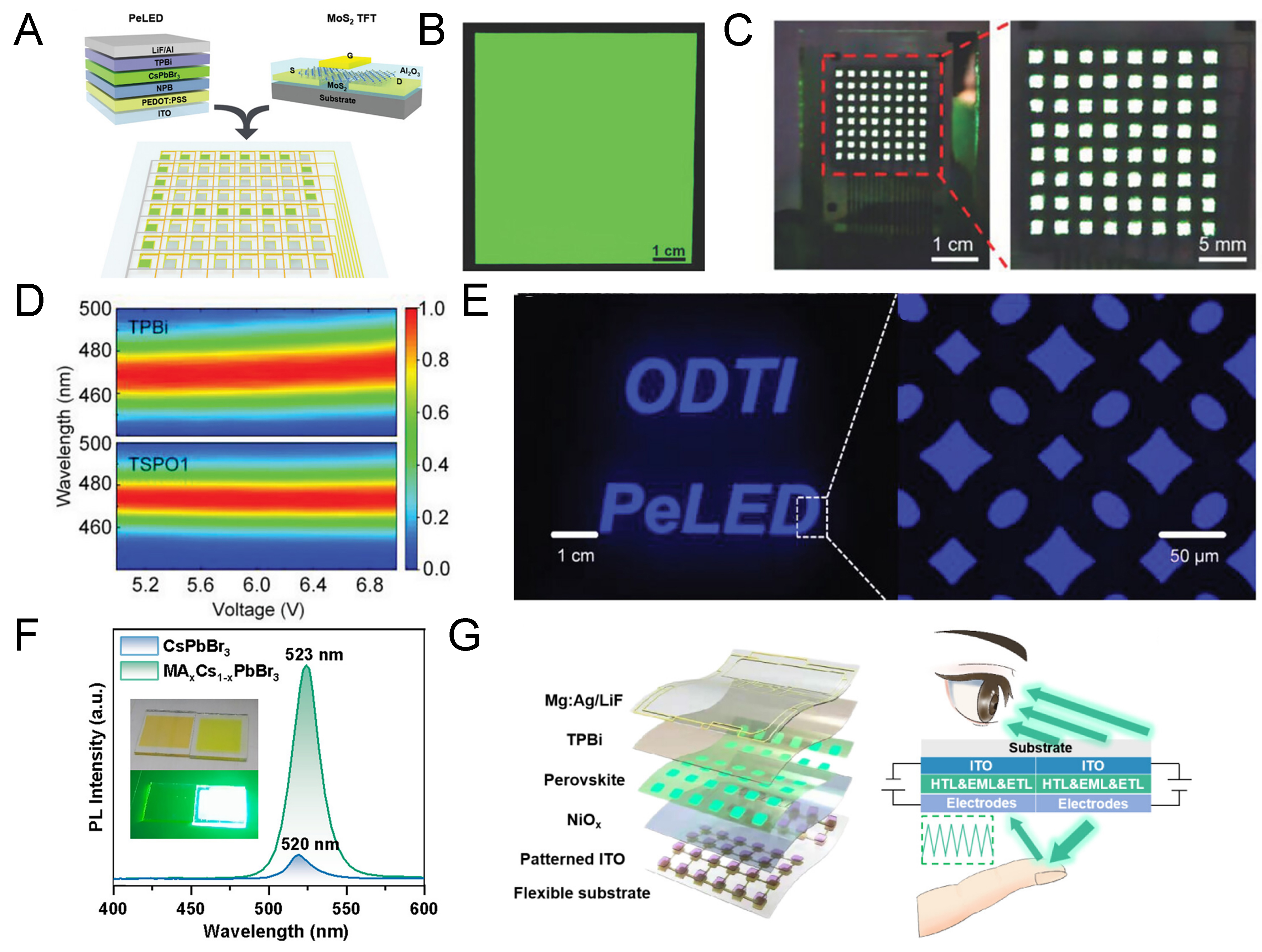
Figure 11. Images of applications fabricated by vacuum deposition. (A) Schematic illustration of integrating vacuum-deposited PeLEDs with MoS3-based TFTs; (B) Optical image of perovskite films deposited on a large-area substrate[151]. Copyright 2024 John Wiley & Sons; (C) Device image showing all pixels in the on-state; (D) Spectral stability of devices with two different electron transport layers as a function of voltage; (E) Optical image of a TSPO1-based top-emitting LED integrated with a TFT[153]. Copyright 2024 John Wiley & Sons; (F) PL spectra of CsPbBr3 with and without MABr incorporation; (G) Schematic illustration of LEDs capable of both top and bottom emission and their application in a heart-rate sensor[156]. Copyright 2024 American Chemistry Society. PeLED: Perovskite light-emitting diode; MoS2: molybdenum disulfide; TFT: thin-film transistor; TSPO1: 2-(4-tert-butylphenyl)-5-(4-biphenylyl)-1,3,4-oxadiazole; PL: photoluminescence; CsPbBr3: cesium lead bromide; MABr: methylammonium bromide.


