




Screen printing as a scalable manufacturing approach for thermoelectric devices
 0
0 Abstract
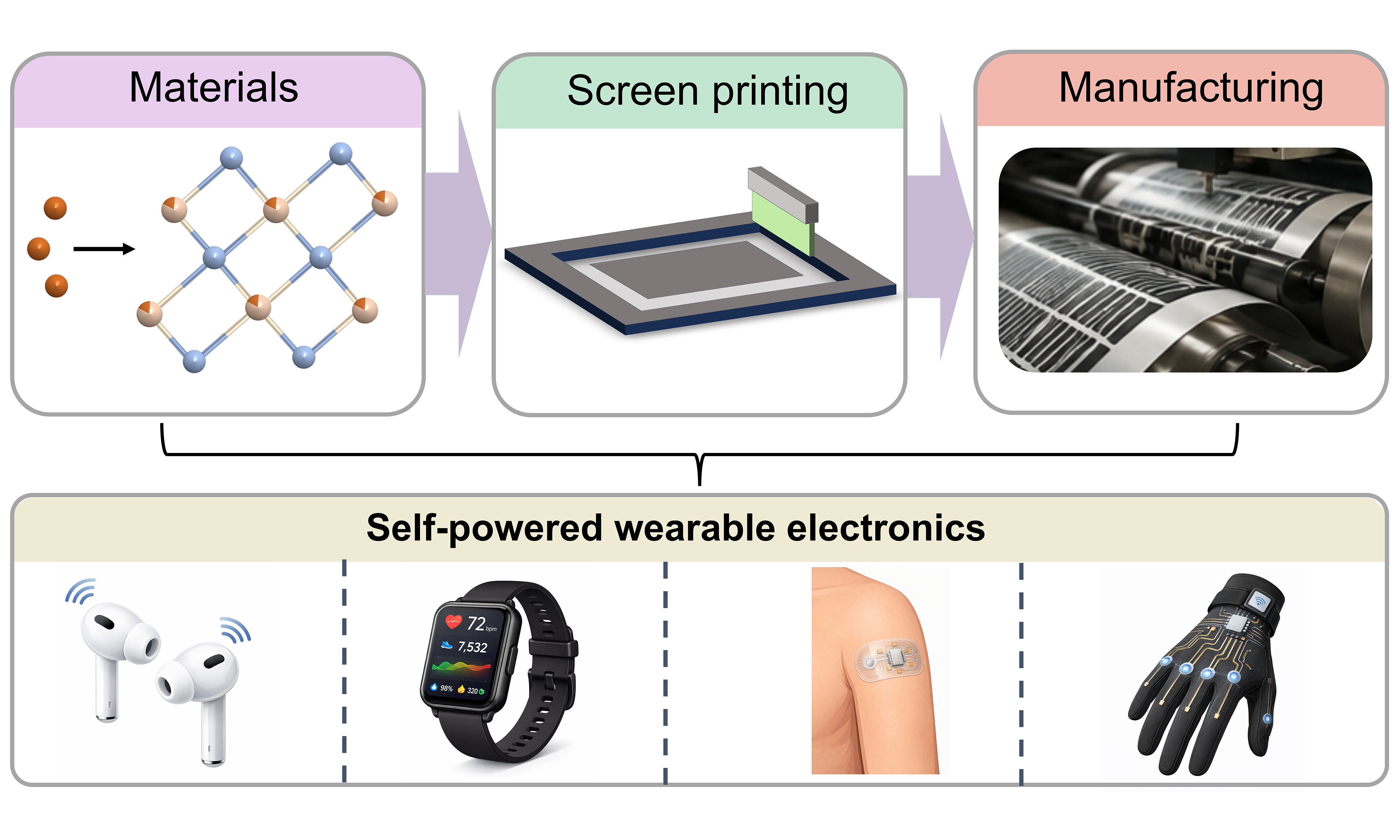
Thermoelectric technology is widely regarded as a promising solution for next-generation energy harvesting and thermal management. To date, extensive efforts have been devoted to enhancing the intrinsic performance of thermoelectric materials, as well as to optimizing device structures and configurations. However, comparatively less attention has been paid to translating these high-performance materials into scalable industrial applications. This paper highlights screen printing as a critical bridge between laboratory-scale research and industrial manufacturing of thermoelectric devices (TEDs), particularly for wearable electronics. We provide a unique and comprehensive overview of the versatility of screen printing across a broad range of thermoelectric materials and device architectures. Furthermore, a systematic fabrication framework is proposed and discussed, offering practical guidelines for constructing TEDs with diverse structural designs via screen printing. This approach enables application-oriented device engineering and facilitates the realization of targeted performance outcomes in real-world scenarios.
Keywords
INTRODUCTION
Thermoelectric technology enables the direct interconversion between heat and electricity via the Seebeck, Peltier, and Thomson effects, offering a solid-state solution for waste heat recovery, localized power generation, and thermal management[1,2]. A typical thermoelectric device (TED) comprises n-type and p-type thermoelectric legs that are electrically connected in series and thermally coupled in parallel[1-3]. Although the output performance of a TED can be partially optimized through geometric design of the thermoelectric legs, its ultimate conversion efficiency (η) is fundamentally constrained by the intrinsic properties of the thermoelectric materials[4]. The performance of thermoelectric materials is commonly evaluated by the dimensionless figure of merit, ZT, defined as ZT = S2σT/κ, where S denotes the Seebeck coefficient, σ the electrical conductivity, κ the thermal conductivity, and T the absolute temperature[4,5]. Due to the strong temperature dependence of charge carrier and phonon transport, different thermoelectric materials exhibit peak ZT values within distinct temperature ranges[5]. Accordingly, thermoelectric materials are generally classified into room-temperature, mid-temperature, and high-temperature systems[6]. For example, Bi2Te3-based alloys dominate near-room-temperature applications (≈ 300-500 K), GeTe- and SnSe-based materials perform effectively in the mid-temperature regime (≈ 400-700 K), whereas oxide- and perovskite-based materials are more suitable for high-temperature operation (> 800 K)[6-8].
Over the past decade, substantial advances in band engineering, defect modulation, and nanostructuring have driven remarkable enhancements in thermoelectric performance. Peak ZT values exceeding 1.9 have been achieved in state-of-the-art Bi-Sb-Te alloys near room temperature, while record average ZT values approaching 3 have been reported in single-crystalline SnSe within the mid-temperature regime[9,10]. Despite these impressive laboratory-scale accomplishments, the large-scale industrial deployment of thermoelectric technologies remains limited[11,12]. A critical bottleneck lies not solely in intrinsic material performance, but rather in the high cost, processing complexity, and limited scalability associated with conventional device fabrication strategies[12,13]. Most advances in thermoelectric research continue to emphasize material-centric optimization, concentrating on crystal structure engineering, electronic band modulation, and phonon transport suppression to maximize ZT[5,14]. Laboratory-scale demonstrations are typically conducted on small-area specimens or proof-of-concept devices, where considerations such as fabrication scalability, manufacturing yield, and system-level integration remain secondary[15,16]. In contrast, successful industrial deployment requires manufacturable device architectures, compatibility with large-area processing, high process reliability, and cost-effective production strategies[11,16]. This fundamental misalignment between laboratory research priorities and industrial manufacturing requirements has significantly impeded the effective translation of high-performance thermoelectric materials into practical technologies, as schematically illustrated in Figure 1[12,13,17-19].
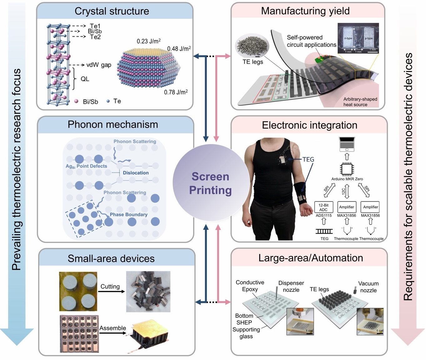
Figure 1. Schematic illustration of the fundamental mismatch between laboratory research priorities and industrial manufacturing requirements, motivating screen printing as a scalable interface for thermoelectric device (TED) fabrication. Inset images include: Bi2Te3-based crystal structure; Reproduced with permission[17]. Copyright 2026, Wiley. Phonon transport mechanism; Reproduced with permission[18]. Copyright 2023, Elsevier. Small-area proof-of-concept devices; Reproduced with permission[19]. Copyright 2025, Royal Society of Chemistry. Manufacturing yield; Large area/automated production; Reproduced under a Creative Commons Attribution 4.0 International License[13]. Copyright 2020, Springer Nature. Electronic system integration; Reproduced with permission[12]. Copyright 2024, Wiley. QL: Quintuple layer; TE: thermoelectric; TEG: thermoelectric generator; SHEP: soft heat transfer and electrical interconnection platform.
Screen printing represents a compelling yet underexplored strategy to bridge this translational gap[3,16]. As a mature, cost-effective, and scalable manufacturing technology, screen printing has been extensively adopted across industries, including batteries, photovoltaics, printed electronics, and sensors[16]. Notably, it offers several intrinsic advantages that align closely with the requirements of TED fabrication[20]. Screen printing accommodates a wide thickness range, from micrometer-scale films to millimeter-scale thick layers, supports powders with diverse compositions, morphologies, and particle sizes, and enables seamless scaling from laboratory prototyping to industrial production[20-23]. Collectively, these attributes position screen printing not simply as an alternative processing route, but as a strategic manufacturing platform that effectively bridges fundamental material innovation with device-level implementation[24].
Recent reviews on flexible, printed, and wearable thermoelectrics have provided comprehensive summaries of material systems, device performance, printing methods, and application prospects. In contrast, this paper does not aim to provide another progress-oriented review. Instead, it reframes screen printing as a manufacturing interface that connects laboratory-scale thermoelectric materials to industrially relevant device fabrication. Specifically, we focus on three interrelated aspects that have received less systematic attention: a material-agnostic processing window for diverse thermoelectric inks, a geometry-enabled design space spanning film-based and bulk-like architectures, and an application-driven decision-making framework for selecting device structures according to practical constraints. This paper highlights how screen printing can move thermoelectric research from material-centric optimization toward manufacturing-informed device design. In this work, we propose screen printing as an effective manufacturing interface that bridges laboratory-scale thermoelectric research with industrial device requirements. We first discuss thermoelectric material systems, encompassing both inorganic and organic materials, that are compatible with screen-printing processes, together with key considerations in ink formulation and processing. We then examine screen-printing-enabled device architectures and the associated structural design flexibility they offer. Finally, we introduce a decision-making framework that links target applications with appropriate printing strategies, device configurations, and anticipated system-level performance outcomes. By shifting the emphasis from material performance alone to manufacturable design pathways, this work seeks to provide practical guidance for accelerating the industrial translation and large-scale deployment of thermoelectric technologies.
MATERIAL-AGNOSTIC PROCESSING WINDOW FOR SCREEN-PRINTED THERMOELECTRIC
Screen printing is a mature and widely adopted manufacturing technology across multiple industries, capable of processing both inorganic and organic materials on diverse substrates through precise control of key processing parameters[25-28]. In the field of thermoelectrics, it similarly establishes a material-agnostic processing window, within which materials of varied compositions, morphologies, and physical properties can be formulated into printable thermoelectric inks, as schematically illustrated in Figure 2[20,29-34]. Besides, a summary of state-of-the-art screen-printed thermoelectric materials is shown in Table 1, indicating the broad compatibility of the screen-printing technique in thermoelectric materials. Printable thermoelectric inks can be systematically engineered by tailoring mesh counts, squeegee shapes, angle of printing, ink rheology, particle size distribution, and interfacial chemistry, thereby enabling the fabrication of both thin-film configurations and thick, bulk-like thermoelectric architectures[20,21,35,36]. Notably, this versatility arises not from material-specific optimization, but from the intrinsic process adaptability of screen printing itself[29-31]. Such characteristics align closely with the fundamental requirements of industrial deployment (including process reliability, scalability, and cost-effectiveness), thereby positioning screen printing as a strategic manufacturing interface that bridges laboratory-scale thermoelectric material innovation with industrially relevant device fabrication.

Figure 2. Material-agnostic processing window for screen-printed thermoelectrics. Schematic illustration showing how ink rheology, particle characteristics, and interfacial modification collectively define a microstructure-preserving printability window, enabling diverse inorganic and organic thermoelectric materials to be translated into screen-printed films. Inset images of inorganic materials: Left; Reproduced with permission[20]. Copyright 2025, Wiley. Right: Reproduced under a Creative Commons Attribution 4.0 International License[29]. Copyright 2024, Springer Nature. Inset images of organic materials: Left; Reproduced with permission[30]. Copyright 2024, Wiley. Right; Reproduced under a Creative Commons Attribution 4.0 International License[31]. Copyright 2022, Wiley. Ink rheology; Reproduced with permission[32]. Copyright 2021, Elsevier. Particle size; Reproduced with permission[33]. Copyright 2024, Springer Nature. Interface modification; Reproduced with permission[34]. Copyright 2019, Wiley.
Summary of state-of-the-art screen-printed thermoelectric materials
| Materials | Ink system | Substrate | Thickness (μm) | Post-treatment temperature (°C) | S 2 σ (μW cm−1 K−2) | κ (W m−1 K−1) | ZT | Ref. |
| p-type: Bi0.5Sb1.5Te3 n-type: Bi2Te2.7Se0.3 | Ethyl cellulose/Butyl carbitol acetate | Al2O3 | 650 | 500 | p-type: 25.6 n-type: 25.9 | p-type: 0.87 n-type: 0.88 | p-type: 0.88 n-type: 0.57 | [37] |
| Bi2Te2.7Se0.3 | Nitrocellulose/BCA | Ceramic | 600 | 500 | 17.2 | 0.65 | 0.88 | [38] |
| PbTe-SrTe | Disperbyk-110/α-terpineol | Alumina | 100 | 700 | 13.8 | 0.82 | 1 | [39] |
| p-type: Bi0.5Sb1.5Te3 n-type: Bi2Te2.7Se0.3 | Polypropylene glycol diglycidyl ether epoxy resin/methylhexahy-drophthalic anhydride | Polyimide | - | 300 | p-type: 3.21 n-type: 1.24 | - | - | [40] |
| Bi2Te3 | Ethyl cellulose/terpineol | Polyimide | - | 350 | 3.63 | 0.586 | 0.2 | [41] |
| p-type: Sb2Te3 n-type: Bi2Te2.7Se0.3 | Polypropylene glycol diglycidyl ether/epoxy resin | Polyimide | 75 | 300 | p-type: 1.5 n-type: 0.6 | - | - | [42] |
| Bi0.4Sb1.6Te3 | Disperbyk-110/α-terpineol | Polyimide | 27 | 450 | 30 | 0.9 | 1 | [34] |
| Bi2Te3 | Ethyl cellulose/diethylene glycol butyl ether acetate/dibutyl phthalate | Polyimide | 166 | 400 | 4.65 | - | - | [43] |
| p-type: Bi0.5Sb1.5Te3 n-type: Bi2Te2.7Se0.3 | PVP/N-methyl-2-pyrrolidone | Glass | 25 | 70 | p-type: 16 n-type: 10.5 | p-type: 0.62 n-type: 0.47 | p-type: 1.45 n-type: 0.75 | [44] |
| Bi0.5Sb1.5Te3 | Epoxy resin/methylhexahydrophthalic anhydride/2-ethyl-4-methylimidazole | Polyimide | 45 | 300 | 15.1 | - | - | [45] |
| Bi0.5Sb1.5Te3 | Epoxy resin/methylhexahydrophthalic anhydride/2-ethyl-4-methylimidazole | Polyimide | 139 | 300 | 24.7 | 0.78 | 0.91 | [46] |
| Bi2Te2.7Se0.3 | Ethyl cellulose/α-terpineol | Polyimide | 3 | 450 | 7.45 | 0.78 | 0.5 | [47] |
| Sb2Te3 | Ethylenediamine | Si/SiO2 | 91 | 180 | - | - | 1.04 | [33] |
| Bi0.4Sb1.6Te3 | Disperbyk-110/α-terpineol | Polyimide | - | 250 | 35 | 0.77 | 1.3 | [48] |
| Ag2Se | Ethanol | Nylon | 5.4 | 200 | 18.82 | 0.696 | 0.8 | [49] |
| Ag-Se-based | Methyl cellulose/thermoplastic resin | Glass | 25 | 300 | 5.4 | 0.28 | 0.6 | [50] |
| Ag2Se | Polystyrene-toluene | Glass | 25 | 200 | 17 | 0.5 | 1.03 | [51] |
| Ag2Se | N-methyl-2-pyrrolidone | Polyimide | 13 | 200 | 13 | 0.45 | 0.92 | [52] |
| Ag2Se | Methyl cellulose/water | Nylon | 30 | 180 | 30.02 | - | - | [53] |
| Ag2Se | Methyl cellulose/water | Nylon | - | 290 | 16.41 | - | - | [35] |
| Ag2Se | α-terpineol | Nylon | - | 200 | 15.5 | 0.57 | 0.8 | [36] |
| Ag2Se/carbon | PVP/ethylene glycol | Polyimide | - | 450 | 16.17 | - | - | [25] |
| Ag2Se/carbon | PVP/ethylene glycol | Polyimide | 10 | 450 | 17.61 | 0.66 | 0.81 | [23] |
| p-type: Cu2Se n-type: Ag2Se | - | Polyimide | p-type: 20.6 n-type: 9.38 | 150 | p-type: 0.42 n-type: 4.68 | p-type: 0.283 n-type: 0.3 | p-type: 0.07 n-type: 0.51 | [54] |
| Cu2Se | Methyl cellulose/water | Nylon | 7.11 | 290 | 1.22 | - | - | [55] |
| CuAgSe | MC/water | Glass fiber fabric | 20 | 350 | 18 | 0.95 | 0.48 | [20] |
| Cu0.6Ni0.4 | Ethyl cellulose/glycerol/EG | Si | 5 | 500 | 28.64 | - | - | [56] |
| p-type: SnSe n-type: Sn0.98Bi0.02Se0.97Te0.03 | CAP/diacetone alcohol | PET | 72 | 400 | - | - | - | [57] |
| Graphene | Ethyl cellulose/terpineol | Polyimide | 2.5 | 350 | - | - | - | [58] |
| ChNCs/MWCNT | Water | Paper | 8 | - | 0.0045 | - | - | [31] |
| PANI/Graphite | Cellulose acetate/diacetone alcohol | polyester | 2.5 | - | - | - | - | [59] |
| PBFDO | - | Kapton | 1.7 | 120 | 0.07 | 2.2 | - | [30] |
Fundamental processing parameters of screen printing
The key processing parameters in screen printing include mesh count, squeegee pressure, and squeegee angle, which strongly influence the properties of the printed films, including thickness, uniformity, and pattern fidelity[60-62]. The selection of these parameters is primarily guided by the characteristics of the ink, the type of substrate, and the required level of pattern detail[61,63].
Ink properties play a central role in determining suitable printing conditions. High-viscosity inks, such as plastisol, typically require lower mesh counts (110-156), moderate squeegee pressures (20-25 N), and relatively low angles (around 45°) to ensure adequate ink transfer and coverage[60-62]. In contrast, low-viscosity inks, such as water-based formulations, benefit from higher mesh counts (≥ 230), higher squeegee pressures (25-35 N), and steeper angles (around 75°) to control ink flow and prevent excessive penetration into the substrate[62,64,65]. Metallic inks, which contain larger particles, generally require even lower mesh counts (38-86), along with reduced pressure (15-20 N) and lower angles to accommodate particle size and maintain print quality[62,64,65].
In addition to ink properties, substrate characteristics are a critical factor in parameter selection. Screen-printing substrates can be broadly categorized into textiles, smooth surfaces, and rough surfaces[62,65]. Textiles, such as fabrics, typically require lower mesh counts (110-156) to compensate for ink absorption and surface porosity. In contrast, smooth substrates, including paper and plastics, allow for higher mesh counts (230-305), enabling finer feature definition and improved pattern resolution[62].
Beyond conventional printing quality, these parameters are particularly critical for thermoelectric inks because they directly influence electrical percolation, porosity evolution, and interparticle transport pathways. Thermoelectric inks typically require relatively high particle loading (commonly > 60-80 wt.% for inorganic systems) to establish continuous conductive networks and preserve thermoelectric transport, whereas excessive binder content, although beneficial for printability and adhesion, may introduce insulating interfaces that reduce σ. Accordingly, most reported systems maintain the combined binder and solvent content below ~ 20 wt.%[36,47,48,54,66]. Similarly, commonly reported viscosity windows for thermoelectric inks range from 1000 to 5000 mPa·s, balancing mesh transfer and pattern fidelity with particle dispersion, densification, and microstructure evolution during post-treatment[66]. Insufficient densification can lead to high porosity and poor electrical contact between thermoelectric particles, ultimately increasing internal resistance and degrading device-level performance. Additionally, solvent selection and drying conditions play an important role in determining film formation and thermoelectric performance. Solvents with different volatilities and boiling points can significantly influence evaporation kinetics during drying, thereby affecting particle redistribution, film uniformity, and microstructure evolution[31,64]. Uncontrolled solvent evaporation may induce thickness non-uniformity and coffee-ring effects, leading to spatial variations in σ and S across the printed film[64]. Therefore, appropriate solvent selection and drying control are essential for achieving homogeneous thermoelectric films with reproducible transport properties and device performance. Therefore, thermoelectric-specific screen-printing windows must balance printability with electrical continuity, microstructure preservation, and interfacial transport.
Inorganic thermoelectric within the screen-printing processing window
Inorganic thermoelectric materials generally exhibit superior thermoelectric performance; however, their development has traditionally proceeded along two largely independent fabrication routes. Bulk thermoelectric materials are typically produced via powder-based approaches, including solvothermal synthesis[18,20,67], melt processing[8,9], and ball milling[68,69]. In contrast, thermoelectric thin films are commonly fabricated using vacuum-based techniques, such as magnetron sputtering[70,71], co-evaporation[72], and other physical vapor deposition (PVD) methods[73,74]. This inherent separation between bulk and thin-film processing pathways not only limits process compatibility but also complicates device integration, thereby posing substantial challenges for scalable and cost-effective manufacturing.
Screen printing provides a distinct advantage by integrating these traditionally separated material forms within a unified, powder-based processing framework[20,29-34,75]. Powders synthesized via conventional bulk-material routes can be directly utilized as printable feedstocks, enabling the fabrication of both bulk-like thick films and thin-film thermoelectric components through careful control of particle morphology and size distribution[34,66]. Importantly, this strategy preserves the microstructural features responsible for high thermoelectric performance, while simultaneously introducing enhanced design flexibility at the device level[41,47]. For instance, CuAgSe powders with dendritic, topology-driven micro-nano architectures synthesized through solution-based methods inherently generate hierarchical structures and complex grain boundary networks during post-printing densification, resulting in suppressed lattice thermal conductivity (κl)[20]. These microstructural characteristics can be effectively retained and incorporated into TED architectures via screen printing[20]. Similarly, solution-synthesized n-type Bi2Te3 nanorods and nanoplates, as well as p-type Bi0.4Sb1.6Te3 nanoparticles prepared by ball milling, have been successfully processed into high-performance thermoelectric films using screen-printing techniques[3,30]. Collectively, these examples demonstrate that the compatibility of screen printing with diverse inorganic thermoelectric powders is not material-dependent but fundamentally enabled by the adaptability of the printing process itself. However, most inorganic thermoelectric films require post-printing annealing or sintering at relatively high temperatures, commonly ranging from 200 to 500 °C, as summarized in Table 1. Consequently, substrate selection for inorganic screen-printed thermoelectric is often limited to thermally stable materials such as polyimide, ceramics, Al2O3, glass, and SiO2. Although screen printing provides a material-agnostic processing pathway, this high-temperature requirement restricts compatibility with low-cost polymer substrates and roll-to-roll manufacturing processes, thereby limiting scalability and increasing manufacturing complexity. Addressing the trade-off between high-temperature densification and substrate compatibility therefore remains a critical challenge for translating laboratory-scale inorganic thermoelectric materials into industrial manufacturing.
By bridging bulk-derived powders with film-based device architectures within a unified manufacturing framework, screen printing significantly reduces fabrication complexity, development cycles, and associated production costs. These advantages align closely with industrial demands, reinforcing the role of screen printing as an effective manufacturing interface for inorganic thermoelectric systems. Nevertheless, the continued reliance on particle-based inks and high-temperature densification processes constrains precise microstructural control and may limit large-scale manufacturing efficiency. This highlights the necessity for advanced strategies that can preserve bulk-level carrier transport properties while enabling scalable fabrication of screen-printed thermoelectric films.
Organic thermoelectric enabled by low-temperature screen printing
Compared with inorganic thermoelectric materials, organic thermoelectrics offer intrinsic advantages in cost-effectiveness, mechanical flexibility, and biocompatibility[76-79]. Owing to their polymeric nature, organic thermoelectric materials are inherently well suited to screen-printing processes, allowing precise tuning of ink rheology, low-temperature film formation, and the fabrication of mechanically compliant thick-film architectures[59,80]. In contrast, inorganic thermoelectric inks typically consist of particulate suspensions that may suffer from dispersion instability and generally require high-temperature sintering, thereby restricting substrate selection and complicating device integration[41,49,81].
The low-temperature processing characteristics of organic thermoelectrics substantially broaden the accessible manufacturing window for screen-printed TEDs. For example, n-type poly(benzodifurandione) (PBFDO) can be fabricated into uniform thermoelectric films via screen printing, followed by mild thermal annealing at approximately 100-120 °C[30]. The resulting films and devices demonstrate excellent environmental stability across a wide temperature range (-8 °C to 200 °C) and under high-humidity conditions (up to 90% relative humidity), underscoring the structural robustness and practical viability of screen-printed organic thermoelectric architectures[30].
Beyond purely organic systems, the low thermal budget associated with screen printing further enables the integration of organic thermoelectric materials with bio-derived and flexible components, giving rise to hybrid thermoelectric systems that are inaccessible through conventional high-temperature processing routes. Such hybridization facilitates direct printing onto a wide range of flexible substrates (including polymer films, textiles, and paper), thereby enabling conformal contact with human skin and highlighting strong potential for wearable thermoelectric applications[27,31,76]. For example, hybrid thermoelectric films composed of multiwall carbon nanotubes (MWCNTs) and chitin nanocrystals (ChNCs) have been successfully fabricated on cellulose paper substrates via screen printing[31]. As naturally derived nanomaterials extracted from shrimp and crab shells, ChNCs impart intrinsic biocompatibility to the printed devices while preserving functional thermoelectric performance[31]. Collectively, these examples demonstrate that the compatibility of screen printing with organic and hybrid thermoelectric materials is not incidental, but fundamentally enabled by its low-temperature, rheology-governed processing characteristics.
By extending the screen-printing processing window beyond rigid inorganic systems to encompass flexible, biocompatible, and hybrid materials, screen printing establishes a versatile manufacturing interface for emerging thermoelectric applications, particularly in wearable and human-centric energy harvesting. Future progress will require concurrent enhancement of σ and thermal stability while preserving low-temperature processability, thereby enabling the development of integrated hybrid organic-inorganic printing platforms for scalable TED fabrication.
Processing parameters defining material compatibility and printability
The material compatibility of screen printing across diverse thermoelectric systems can be rationalized within a unified processing window defined by three interrelated parameters: ink rheology, particle attributes, and interfacial chemistry[20,29,32,34]. Rather than being material-specific, printability arises from the dynamic balance among viscous, capillary, and interfacial forces that govern ink transfer, mesh filling, and pattern fidelity during the printing process[82]. This balance can be quantitatively described using dimensionless relationships that couple surface tension (γ), viscosity (η), and printing speed (U). In particular, the capillary number (Ca) provides a generalized framework for predicting printable regimes across different material systems, thereby establishing a process-based criterion for screen-printing compatibility[82]. Here,
Particle size and morphology play a dual role within this processing framework. They influence not only the ability of the ink to infiltrate the screen mesh and form continuous, thickness-controlled films, but also the microstructural evolution during post-printing densification, which ultimately governs thermoelectric transport properties[47,83]. Carefully engineered particle size distributions facilitate uniform film formation while preserving critical microstructural features, such as grain boundaries and hierarchical architectures, that contribute to reduced κl and optimized carrier transport[20]. For example, Sb2Te3 inks formulated with smaller particle sizes yield films with superior thickness uniformity and enhanced thermoelectric performance compared with those derived from coarser powders, underscoring the importance of particle-size-controlled film formation[33].
Interfacial modification further broadens the printable processing window by mitigating the intrinsic porosity and weak interparticle contacts commonly observed in screen-printed films[34,41]. The incorporation of organic binders and conductive polymers can enhance film continuity and reduce porosity; for example, introducing acid-doped polyaniline (PANI) into Cu2Se inks significantly decreases film porosity while simultaneously improving the power factor (S2σ)[83]. In parallel, inorganic nanosolders and secondary phases can facilitate densification and strengthen interfacial coupling without compromising electronic transport[34,47]. For instance, the addition of Te into Bi-Sb-Te systems suppresses defect formation and promotes sintering, enabling screen-printed films to achieve thermoelectric performance comparable to, or even surpassing, that of conventionally processed bulk counterparts[34,47,48]. Importantly, these strategies extend beyond simple improvements in film integrity; they enable the retention or even enhancement of thermoelectric performance through deliberate tuning of carrier filtering effects, contact resistance, and phonon scattering mechanisms.
These considerations underscore a critical distinction for thermoelectric systems: printability alone is insufficient. A truly material-agnostic processing window must not only enable pattern formation, but also preserve the microstructural features that govern thermoelectric transport. However, the establishment of quantitative printability metrics that explicitly correlate rheological parameters with transport performance remains an open challenge for predictive thermoelectric manufacturing. Defining microstructure-preserving printability would provide a rigorous and predictive framework for translating diverse thermoelectric materials into screen-printed architectures, thereby laying the foundation for the device-level design strategies discussed in the following section.
ARCHITECTURE DESIGN OF DEVICES ENABLED BY SCREEN PRINTING
Beyond material compatibility, the defining advantage of screen printing lies in its concurrent control over film thickness and lateral resolution, which together establish a continuous geometric design space for TEDs[20,21]. Rather than constituting two discrete categories, film-based and bulk-like architectures can be regarded as limiting cases within this continuum, spanning from planar thin-film geometries with high pattern fidelity to vertically stacked, thick architectures with substantial cross-plane dimensions. In film-based configurations, thermoelectric elements are laterally defined through mesh-controlled patterning and rheology-governed ink flow, enabling large-area coverage, operation under small temperature differences (ΔTs), and seamless integration with flexible substrates[35,54]. By contrast, bulk-like architectures are realized through layer-by-layer deposition of thick thermoelectric units, facilitating three-dimensional (3D) stacking, increased leg thickness, and improved tolerance to large thermal gradients[21,84]. This geometry-enabled design flexibility positions screen printing as a versatile platform for tailoring TED architectures to application-specific requirements, as illustrated in Figure 3[20,21,31,37,66,85]. Table 2 summarizes the most recent screen-printed TEDs.

Figure 3. Screen-printing-enabled geometric design space for TEDs. Film-based architectures: (A) Wearable CuAgSe thermoelectric arrays fabricated on flexible substrates for body-heat harvesting. Reproduced with permission[20]. Copyright 2025, Wiley; (B) Pattern-defined thermoelectric tracks demonstrating circuit-level integration on diverse substrates. Reproduced under a Creative Commons Attribution 4.0 International License[31]. Copyright 2022, Wiley; (C) High-resolution micro-thermoelectric generators featuring radially defined p-n geometries. Reproduced with permission[85]. Copyright 2019, Elsevier; Bulk-based architectures: (D) Vertically integrated p-n arrays on ceramic substrates enabled by layer-by-layer printing and hybrid microfabrication. Reproduced with permission[37]. Copyright 2017, Royal Society of Chemistry; (E) Semi-flexible multilayer TEDs fabricated on paper-based substrates. Reproduced with permission[66]. Copyright 2023, Wiley; (F) Stacked thermoelectric modules incorporating interfacial layers for contact-resistance reduction. Reproduced under a Creative Commons Attribution 3.0 International License[21]. Copyright 2025, Royal Society of Chemistry. CCNT: Chitin nanocrystals/multiwalled carbon nanotube; PET: polyethylene terephthalate; TE: thermoelectric; UV: ultraviolet.
Summary of screen-printed TEDs
| Architecture | ΔTmax (K) | Pairs | P (mW) | ω (mW cm-2) | Ref. |
| Bulk-based | 28 | 200 | 310 | 7.34 | [37] |
| Bulk-based | 25.6 | 72 | - | 6.32 | [38] |
| Bulk-based | 40 | 80 | 0.94 | - | [66] |
| Bulk-based | 50 | 24 | - | 0.04787 | [86] |
| Bulk-based | 10 | 60 | - | 0.069 | [84] |
| Bulk-based | 60 | 42 | - | 0.234 | [54] |
| Bulk-based | 43 | 50 | 1.22 | 0.067 | [21] |
| Film-based | 61.2 | 21 | 0.00011 | 0.00269 | [30] |
| Film-based | 29.5 | 800 | - | 0.015 | [47] |
| Film-based | 28.3 | 5 | 0.000923 | 0.606 | [47] |
| Film-based | 9.5 | 4 | 0.00000671 | 0.00472 | [55] |
| Film-based | 68 | - | - | 0.51 | [44] |
| Film-based | 10 | - | 0.24 | 0.000024 | [87] |
| Film-based | 48.3 | 5 | 0.00631 | - | [40] |
| Film-based | 80 | 4 | 0.054 | 18.8 | [34] |
| Film-based | 48 | 50 | 0.114 | 0.514 | [85] |
| Film-based | 105 | 1 | 0.0271 | 3.265 | [43] |
| Film-based | 30 | 4 | 0.0032 | 2.2 | [49] |
| Film-based | 110 | 13 | - | 0.321 | [50] |
| Film-based | 75 | 2 | 0.00019 | - | [51] |
| Film-based | 188.4 | 30 | 1.26 | - | [42] |
| Film-based | 80.7 | 21 | 0.37 | - | [52] |
| Film-based | 20 | 5 | - | 0.69 | [53] |
| Film-based | 100 | 8 | - | 0.00238 | [83] |
| Film-based | 97.5 | 6 | 0.84 | 27 | [48] |
| Film-based | 14.1 | 4 | - | 0.351 | [35] |
| Film-based | 35.4 | 4 | - | 2.91 | [25] |
| Film-based | 34.1 | 6 | - | 1.62 | [36] |
| Film-based | 140 | 4 | 0.000583 | - | [56] |
| Film-based | 137 | 8 | 0.000008 | - | [88] |
| Film-based | 120 | 8 | 0.000007 | - | [57] |
| Film-based | 31.4 | 4 | 0.0055 | 2.29 | [23] |
| Film-based | 7 | 132 | 0.002 | - | [20] |
Film-based architectures
Film-based TEDs represent the planar limit of the screen-printing design space and are typically fabricated on flexible substrates to enable conformal integration with curved or soft surfaces. Their lateral geometry facilitates large-area coverage and efficient operation under small ΔTs, making them particularly well-suited for body-heat harvesting and distributed thermal sensing applications. For example, wearable CuAgSe-based arrays printed on textile substrates demonstrate the feasibility of screen-printed thermoelectrics for body-heat harvesting, highlighting the compatibility of planar architectures with flexible and fabric-based platforms (nanofiber membranes, PI, and glass fiber fabrics), as shown in Figure 3A[20]. Beyond energy harvesting, the high pattern fidelity enabled by mesh-controlled printing allows thermoelectric elements to be integrated into circuit-like layouts. Pattern-defined thermoelectric tracks fabricated from printable composite inks composed of ChNCs and MWCNTs illustrate how thermoelectric functionality can be embedded within electronic architectures, thereby enabling multifunctional energy-harvesting and sensing platforms, as shown in Figure 3B[31]. At higher pattern resolutions, micro-thermoelectric generators with radially defined p-n geometries (Sb2Te3/Bi2Te2.7Se0.3), shown in Figure 3C, further demonstrate the capability of screen printing to produce compact, device-level architectures while retaining the advantages of planar heat spreading[85].
Collectively, these examples reveal a resolution-dependent functional regime: low-resolution, large-area patterns tailored for wearable and distributed applications; intermediate-resolution layouts enabling circuit-level integration; and high-resolution micro-architectures designed for compact energy harvesting. This pattern-enabled design flexibility represents a defining feature of screen-printed film-based thermoelectrics, offering a direct pathway to match device geometry with application-specific thermal conditions. Nevertheless, scaling planar architectures toward higher power densities (ω) while preserving mechanical compliance remains a central challenge for wearable and distributed thermoelectric systems.
Bulk-based architectures
Bulk-like TEDs represent the thickness-dominated limit of the screen-printing design space, where cross-plane heat transport and multilayer stacking enable higher ω and operation under larger ΔTs. In this regime, device performance is determined not only by intrinsic material properties but also by structural parameters such as the number of printed layers, leg thickness, and interfacial engineering. As illustrated in Figure 3D, thermoelectric legs fabricated via screen printing can be integrated with sputtered electrodes and conventional bonding processes on ceramic substrates, demonstrating compatibility with established microfabrication workflows and enabling densely packed p-n arrays for compact power-generation
These examples delineate a thickness-dependent functional regime in which increasing the number of printed layers and leg thickness enhances cross-plane thermal gradients and ω, while interfacial engineering critically determines electrical continuity and overall device efficiency. Together with the planar architectures discussed above, bulk-like configurations complete the continuous geometric design space enabled by screen printing, offering a scalable pathway from flexible, low-temperature-gradient systems to compact, high-output thermoelectric modules. Despite these advances, contact resistance remains a central challenge, underscoring the urgent need to develop low-resistance, thermally stable interlayers to realize high-efficiency multilayer thermoelectric modules.
DECISION-MAKING FRAMEWORK FOR APPLICATION-DRIVEN DESIGN
Thermoelectric applications can be broadly categorized into three representative regimes according to their dominant operational constraints: wearable and low-grade heat harvesting, Internet of Things (IoT) and self-powered nodes, and industrial heat-flux recovery. Rather than prescribing fixed device architectures, a decision-making framework can be constructed by systematically mapping these application-specific constraints onto the geometric design space enabled by screen printing, as illustrated in Figure 4.
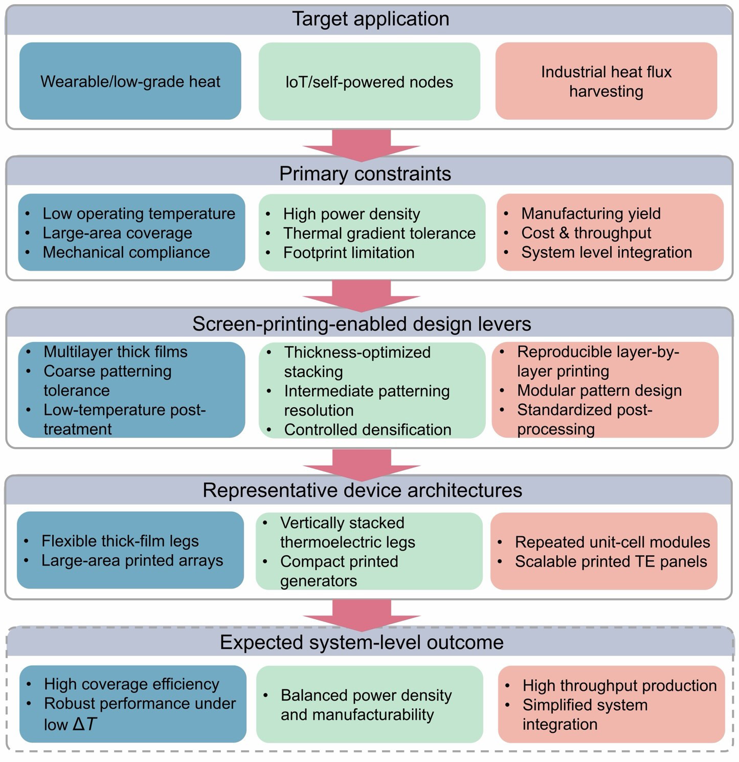
Figure 4. Decision-making framework for application-driven TED design. Schematic illustration of a constraint-driven design flow that maps key application requirements (temperature gradient, device footprint, mechanical flexibility, and target power density) onto the geometric design space enabled by screen printing (lateral resolution and thickness). This mapping facilitates the rational selection of film-based or bulk-like architectures, together with appropriate processing strategies and interfacial engineering approaches. IoT: ΔT: temperature difference; TED: thermoelectric device.
For wearable and low-grade heat-harvesting applications, the primary constraints include small ΔTs, large-area coverage, and mechanical compliance[31,36,44,89]. These requirements favor planar, film-based architectures fabricated on flexible substrates, where lateral patterning enables distributed thermoelectric arrays with precisely controlled pattern fidelity[20,29,48]. For example, because wearable thermoelectric systems typically operate under low ΔTs (< 10-20 °C), maximizing thermal contact area is more beneficial than increasing device thickness. Therefore, planar architectures are generally preferred. A representative example is a 12 × 11 array of CuAgSe thermoelectric legs printed on nanofiber membrane, PI film, and glass fiber fabric substrates, which provides a large contact surface and generates a stable output voltage of approximately 50 mV from body heat[20]. Such geometries maximize surface conformability and user comfort while ensuring stable operation under low ΔT conditions, making them particularly well suited for body-heat harvesting and conformal energy-harvesting platforms[30,50].
In contrast, IoT and self-powered node applications require higher ω within confined device footprints, typically operating under moderate thermal gradients[38,40]. In this regime, thickness-controlled and vertically stacked architectures become advantageous, as increased leg thickness and multilayer integration enhance cross-plane heat transport and overall power output[66,90]. A representative example is a screen-printed vertical TED comprising Ag electrodes and 160 thermoelectric legs deposited on a paper substrate, which achieves an output power of 940.8 μW under a ΔT of 40 °C[66]. However, this configuration introduces additional constraints, particularly increased interfacial resistance and manufacturability challenges associated with multilayer stacking. The central design challenge, therefore, lies in achieving an optimal balance among ω, electrical continuity, and scalable fabrication[21].
For industrial heat-flux harvesting applications, system-level considerations become predominant, including manufacturing yield, cost-effectiveness, and modular integration[11,21]. For example, an additive screen-printing strategy incorporating glass dielectric layers enabled multiple printing cycles of thermoelectric legs while maintaining structural integrity and electrical connectivity, achieving an output power of 1.22 mW under a ΔT of 43 °C[21]. This example demonstrates how process repeatability and modular fabrication can be leveraged to overcome conventional thickness limitations and facilitate scalable thermoelectric manufacturing[21]. Accordingly, the emphasis shifts from optimizing individual device performance to ensuring architectural repeatability, production reliability, and seamless integration into larger thermal management and energy-conversion systems.
Collectively, these regimes demonstrate how application-specific constraints can be systematically mapped onto thickness and resolution parameters within the screen-printing design space. This constraint-driven geometric selection establishes a practical design workflow that links application requirements to architectural configuration, thereby elevating screen printing from a fabrication technique to a predictive manufacturing interface for thermoelectric technologies. Future efforts should extend this framework toward device-system co-design, enabling quantitative performance prediction under realistic thermal boundary conditions and operational environments.
CONCLUSION AND OUTLOOK
The misalignment between laboratory-scale thermoelectric research and industrial manufacturing requirements has remained a fundamental barrier to the large-scale deployment of thermoelectric technologies. In this work, we identify screen printing as a manufacturing interface capable of bridging this gap by offering both a material-agnostic processing window and a geometry-enabled design space for TEDs. By unifying material compatibility, architectural configurability, and application-driven constraints within a single framework, we establish a decision-making strategy that elevates screen printing from a conventional fabrication technique to a predictive and scalable platform for TED development.
Despite this progress, several critical challenges must be addressed to realize manufacturing-informed thermoelectric design. First, the absence of standardized printability metrics limits the transferability of processing conditions across different material systems, underscoring the need for quantitative printability maps that correlate rheology, particle attributes, and film-formation behavior. Second, the performance of screen-printed thermoelectrics is governed by complex processing-microstructure-transport coupling that remains insufficiently understood; establishing a predictive theoretical framework for this interdependence is therefore essential to ensure reproducibility and scalable optimization. Third, multilayer architectures introduce additional interfacial resistance that constrains overall device efficiency, highlighting the necessity for systematic interlayer engineering and the development of scaling laws governing electrical and thermal contacts. Finally, long-term reliability under cyclic thermal and mechanical loading remains largely unexplored and will be crucial for the practical deployment of ink-processed thermoelectric systems.
Looking forward, the advancement of screen-printed thermoelectrics will require coordinated progress in several key areas:
(1) Establishing quantitative printability metrics. The development of standardized printability metrics that link ink rheology, particle characteristics, and printing conditions with film quality and thermoelectric performance will be essential for improving reproducibility and accelerating process optimization.
(2) Building process-structure-transport coupling theories. Future research should establish rigorous frameworks that correlate processing parameters with microstructure evolution and thermoelectric transport properties. Such understanding will facilitate predictive design rather than empirical optimization of screen-printed thermoelectric materials.
(3) Developing interface-engineered device architectures. Advanced multilayer architectures require effective strategies to reduce contact resistance and improve interfacial transport. Interface engineering will therefore play a critical role in enabling high-performance and scalable TEDs.
(4) Enhancing long-term reliability and manufacturability. Reliability-oriented device design, including stability under thermal cycling, mechanical deformation, and long-term operation, will be crucial for translating laboratory-scale demonstrations into practical technologies.
(5) Enabling manufacturing-informed thermoelectric design. Beyond incremental improvements in materials and device configurations, the emergence of manufacturing-informed thermoelectric design has the potential to fundamentally reshape how thermoelectric technologies are conceived, engineered, and deployed. By integrating quantitative printability metrics, process-structure-transport coupling, and geometry-driven architectural strategies, screen printing facilitates a shift from material-centric optimization toward system-aware, multi-scale design. This paradigm creates new opportunities for digital manufacturing, high-throughput device prototyping, and data-driven optimization of thermoelectric modules tailored to specific thermal boundary conditions and operational environments.
In the long term, the convergence of scalable printing, predictive modelling, and modular device integration may enable thermoelectric technologies to transition from laboratory demonstrations to deployable energy-harvesting and thermal-management systems. In this context, screen printing should be regarded not merely as a fabrication technique, but as a potential platform for manufacturing-enabled thermoelectric innovation.
DECLARATIONS
Acknowledgements
This work was enabled by using the Central Analytical Research Facility hosted by the Institute for Future Environments at QUT.
Authors’ contributions
Supervised the whole project: Chen, Z. G.; Shi, X. L.
Prepared the first draft: Chen, W.
Provided the constructive suggestion on the manuscript: Li, M.
Reviewed and edited the manuscript: Chen, W.; Chen, Z. G.; Shi, X. L.
Availability of data and materials
Not applicable.
AI and AI-assisted tools statement
During the preparation of this manuscript, the AI tool ChatGPT (Version 5.5, Release Date: 2026-04-23) was used for language editing, the icons of manufacturing, smartwatch, earphone, skin patches, and smart gloves in the Graphical Abstract were generated specifically for this work using the OpenAI ChatGPT (Version 5.5, Release Date: 2026-04-23) image-generation tool. The tools did not influence the study design, data collection, analysis, interpretation, or the scientific content of the work. All authors take full responsibility for the accuracy, integrity, and final content of the manuscript.
Financial support and sponsorship
The work is supported by the Australian Research Council, HBIS-UQ Innovation Centre for Sustainable Steel project, and the QUT Capacity Building Professor Program.
Conflicts of interest
Chen, Z. G. is the Guest Editor of the Special Topic “Stretchable Thermoelectric: Strategies, Performances, and Applications” and an Editorial Board Member in Soft Science. He had no involvement in the review or editorial process of this manuscript, including, but not limited to, reviewer selection, evaluation, or the final decision, while the other authors have declared no conflicts of interest.
Ethical approval and consent to participate
Not applicable.
Consent for publication
Not applicable.
Copyright
© The Author(s) 2026.
REFERENCES
1. Liu, S.; Bai, S.; Wen, Y.; et al. Quadruple-band synglisis enables high thermoelectric efficiency in earth-abundant tin sulfide crystals. Science 2025, 387, 202-8.
2. Xu, S.; Horta, S.; Lawal, A.; Maji, K.; Lorion, M.; Ibáñez, M. Interfacial bonding enhances thermoelectric cooling in 3D-printed materials. Science 2025, 387, 845-50.
3. Chen, W.; Shi, X. L.; Li, M.; et al. Nanobinders advance screen-printed flexible thermoelectrics. Science 2024, 386, 1265-71.
4. Yang, S.; Qiu, P.; Chen, L.; Shi, X. Recent developments in flexible thermoelectric devices. Small. Sci. 2021, 1, 2100005.
5. Yang, Q.; Yang, S.; Qiu, P.; et al. Flexible thermoelectrics based on ductile semiconductors. Science 2022, 377, 854-8.
6. Shi, X. L.; Zou, J.; Chen, Z. G. Advanced thermoelectric design: from materials and structures to devices. Chem. Rev. 2020, 120, 7399-515.
7. Qin, B.; Kanatzidis, M. G.; Zhao, L. D. The development and impact of tin selenide on thermoelectrics. Science 2024, 386, eadp2444.
8. Liu, C.; Zhang, Z.; Peng, Y.; et al. Charge transfer engineering to achieve extraordinary power generation in GeTe-based thermoelectric materials. Sci. Adv. 2023, 9, eadh0713.
9. Gao, T.; Wen, Y.; Bai, S.; et al. Extending the temperature range of the Cmcm phase of SnSe for high thermoelectric performance. Science 2025, 390, 1266-71.
10. Zhou, M.; Su, H.; Pei, J.; et al. Ultrahigh thermoelectricity obtained in classical BiSbTe alloy processed under super-gravity. Nat. Commun. 2025, 16, 7645.
11. Liu, J. Z.; Jiang, W.; Zhuo, S.; et al. Large-area radiation-modulated thermoelectric fabrics for high-performance thermal management and electricity generation. Sci. Adv. 2025, 11, eadr2158.
12. Zadan, M.; Wertz, A.; Shah, D.; et al. Stretchable thermoelectric generators for self‐powered wearable health monitoring. Adv. Funct. Mater. 2024, 34, 2404861.
13. Lee, B.; Cho, H.; Park, K. T.; et al. High-performance compliant thermoelectric generators with magnetically self-assembled soft heat conductors for self-powered wearable electronics. Nat. Commun. 2020, 11, 5948.
14. Shi, X. L.; Li, N. H.; Li, M.; Chen, Z. G. Toward efficient thermoelectric materials and devices: advances, challenges, and opportunities. Chem. Rev. 2025, 125, 7525-724.
15. Liu, Q.; Shi, X.; Cao, T.; Chen, W.; Li, L.; Chen, Z. Advances and challenges in inorganic bulk-based flexible thermoelectric devices. Prog. Mater. Sci. 2025, 150, 101420.
16. Shi, X. L.; Wang, L.; Lyu, W.; et al. Advancing flexible thermoelectrics for integrated electronics. Chem. Soc. Rev. 2024, 53, 9254-305.
17. Xue, Z.; Huang, X.; Lin, W.; et al. Competing grain growth pathways in anisotropic Bi2Te3-based thermoelectric nanoplates. Adv. Mater. 2026, 38, e10614.
18. Chen, W.; Shi, X.; Yang, Q.; et al. Solvothermally silver doping boosting the thermoelectric performance of polycrystalline Bi2Te3. Chem. Eng. J. 2023, 475, 146428.
19. Yuan, X.; Qiu, P.; Sun, C.; et al. Screening thermoelectric materials for high-output performance in wearable electronics. Energy. Environ. Sci. 2025, 18, 5416-23.
20. Zhou, X.; Li, K.; Hou, C.; Zhang, Q.; Li, Y.; Wang, H. Ligand-free multi-scale CuAgSe micro-nanoparticles with a dendritic structure for application as a room temperature thermoelectric material. Adv. Funct. Materials. 2025, 35, 2505741.
21. Antharam, S.; Khan, M. I.; Franke, L.; et al. Milliwatt-scale 3D thermoelectric generators via additive screen printing. Energy. Environ. Sci. 2025, 18, 7648-59.
22. Zhang, Y.; Zhao, L.; Li, J.; et al. Screen-printed large-area wearable graphene-coated cotton fabric-based thermoelectric generator for solar energy harvesting and health monitoring. Compos. Commun. 2025, 58, 102526.
23. Zhang, M.; Li, J.; Liu, Y.; et al. Screen printing high-performance free-standing Ag2Se/carbon composite film for flexible thermoelectric converters. Nano. Energy. 2025, 138, 110836.
24. Lyu, J.; Zhang, L.; Yang, Y.; Zhu, J.; Shi, X.; Chen, Z. Ag2Se-Based thermoelectric materials and devices: progress, challenges, and perspectives. Energy. Environ. Sci. 2026, 19, 3134-83.
25. Zhang, M.; Liu, Y.; Li, J.; et al. Screen printing Ag2Se/carbon nanocomposite films for flexible thermoelectric applications. Carbon 2024, 229, 119480.
26. Su, H.; Lin, P.; Lu, H.; Chen, Y. Efficient solar-thermal conversion and thermal energy storage towards personal thermal management and thermoelectric power generation enabled by massive screen printing of carbon nanotube dopped energy storage gels. J. Energy. Storage. 2024, 76, 109782.
27. Liao, Y.; Tian, Y.; Ma, X.; Zhao, M.; Qian, J.; Wang, X. Screen-printed high-performance flexible electrothermal films based on three-dimensional intercalation graphene nanosheets/MWCNT/carbon black composite. ACS. Appl. Mater. Interfaces. 2020, 12, 48077-83.
28. Ma, H.; Lu, T.; Shi, X.; et al. Advancements and challenges in printed thermoelectrics. Prog. Mater. Sci. 2026, 158, 101619.
29. Liu, Y.; Zhang, Q.; Huang, A.; et al. Fully inkjet-printed Ag2Se flexible thermoelectric devices for sustainable power generation. Nat. Commun. 2024, 15, 2141.
30. Brunetti, I.; James, Pataki. N.; Hinojosa, D. R.; et al. A scalable fully printed organic thermoelectric generator for harsh environments enabled by a stable n‐type polymer. Adv. Mater. Technol. 2025, 10, 2400968.
31. He, Y.; Lin, X.; Feng, Y.; Luo, B.; Liu, M. Carbon nanotube ink dispersed by chitin nanocrystals for thermoelectric converter for self-powering multifunctional wearable electronics. Adv. Sci. (Weinh). 2022, 9, e2204675.
32. Hong, H.; Jiyong, H.; Moon, K.; Yan, X.; Wong, C. Rheological properties and screen printability of UV curable conductive ink for flexible and washable E-textiles. J. Mater. Sci. Technol. 2021, 67, 145-55.
33. Ruamruk, S.; Chayasombat, B.; Singsoog, K.; Seetawan, T. Thermoelectric properties of Sb2Te3 ink fabricated by screen-printing technique. J. Electron. Mater. 2024, 53, 4111-9.
34. Varghese, T.; Dun, C.; Kempf, N.; et al. Flexible thermoelectric devices of ultrahigh power factor by scalable printing and interface engineering. Adv. Funct. Mater. 2020, 30, 1905796.
35. Xiao, Z.; Meng, Q.; Du, Y.; et al. High-performance Ag2Se/methyl cellulose thermoelectric composites for flexible power generators. Energy. Mater. Adv. 2024, 5, 0103.
36. Zhang, M.; Liu, Y.; Li, J.; et al. Scalable printing high-performance and self-healable Ag2Se/terpineol nanocomposite film for flexible thermoelectric device. Energy 2024, 296, 131232.
37. Choi, H.; Kim, S. J.; Kim, Y.; We, J. H.; Oh, M.; Cho, B. J. Enhanced thermoelectric properties of screen-printed Bi0.5Sb1.5Te3 and Bi2Te2.7Se0.3 thick films using a post annealing process with mechanical pressure. J. Mater. Chem. C. 2017, 5, 8559-65.
38. Kim, S. J.; Choi, H.; Kim, Y.; et al. Post ionized defect engineering of the screen-printed Bi2Te2.7Se0.3 thick film for high performance flexible thermoelectric generator. Nano. Energy. 2017, 31, 258-63.
39. Han, C.; Tan, G.; Varghese, T.; Kanatzidis, M. G.; Zhang, Y. High-performance PbTe thermoelectric films by scalable and low-cost printing. ACS. Energy. Lett. 2018, 3, 818-22.
40. Yuan, Z.; Tang, X.; Xu, Z.; et al. Screen-printed radial structure micro radioisotope thermoelectric generator. Appl. Energy. 2018, 225, 746-54.
41. Feng, J.; Zhu, W.; Deng, Y.; Song, Q.; Zhang, Q. Enhanced antioxidation and thermoelectric properties of the flexible screen-printed Bi2Te3 films through interface modification. ACS. Appl. Energy. Mater. 2019, 2, 2828-36.
42. Yuan, Z.; Tang, X.; Cabot, A.; et al. High-performance micro-radioisotope thermoelectric generator with large-scale integration of multilayer annular arrays through screen printing and stacking coupling. Energy. Tech. 2021, 9, 2001047.
43. Feng, J.; Zhu, W.; Zhang, Z.; Cao, L.; Yu, Y.; Deng, Y. Enhanced electrical transport properties via defect control for screen-printed Bi2Te3 films over a wide temperature range. ACS. Appl. Mater. Interfaces. 2020, 12, 16630-8.
44. Mallick, M. M.; Franke, L.; Rösch, A. G.; et al. High figure-of-merit telluride-based flexible thermoelectric films through interfacial modification via millisecond photonic-curing for fully printed thermoelectric generators. Adv. Sci. (Weinh). 2022, 9, e2202411.
45. Hu, Y.; Nie, X.; Ke, S.; et al. Tuning thermoelectric conversion performance of BiSbTe/epoxy flexible films with dot magnetic arrays. ACS. Appl. Mater. Interfaces. 2023, 15, 7112-9.
46. Ke, S.; Liang, D.; Nie, X.; et al. Multi-beam spark plasma sintering and excellent performance of Bi0.5Sb1.5Te3/epoxy thermoelectric films with insulating substrates. Energy. Environ. Sci. 2023, 16, 5434-43.
47. Shi, J.; Wu, X.; Geng, X.; et al. Anisotropy engineering in solution-derived nanostructured Bi2Te3 thin films for high-performance flexible thermoelectric devices. Chem. Eng. J. 2023, 458, 141450.
48. Tanvir, A. N. M.; Bappy, M. O.; Zeng, M.; et al. High-performance thermoelectric composites via scalable and low-cost ink processing. Energy. Environ. Sci. 2024, 17, 4560-8.
49. Jiang, C.; Ding, Y.; Cai, K.; et al. Ultrahigh performance of n-type Ag2Se films for flexible thermoelectric power generators. ACS. Appl. Mater. Interfaces. 2020, 12, 9646-55.
50. Mallick, M. M.; Rösch, A. G.; Franke, L.; et al. High-performance Ag-Se-based n-type printed thermoelectric materials for high power density folded generators. ACS. Appl. Mater. Interfaces. 2020, 12, 19655-63.
51. Mallick, M. M.; Rösch, A. G.; Franke, L.; et al. New frontier in printed thermoelectrics: formation of β-Ag2Se through thermally stimulated dissociative adsorption leads to high ZT. J. Mater. Chem. A. 2020, 8, 16366-75.
52. Franke, L.; Georg, Rösch. A.; Khan, M. I.; et al. High power density Ag2Se/Sb1.5Bi0.5Te3 ‐based fully printed origami thermoelectric module for low‐grade thermal energy harvesting. Adv. Funct. Materials. 2024, 34, 2403646.
53. Jia, L.; Ai, W.; Gao, J.; et al. Optimization of power factor for a screen-printed silver selenide-based flexible thermoelectric film by hot pressing. ACS. Appl. Energy. Mater. 2024, 7, 5721-7.
54. Zhang, D.; Li, L.; Zhang, X.; et al. In situ synthesized staggered‐layer‐boosted flexible Ag2Se and Cu2Se thin films for wearable thermoelectric power generators. Adv. Funct. Mater. 2025, 35, 2419392.
55. Qin, J.; Du, Y.; Meng, Q.; Ke, Q. Flexible thermoelectric Cu-Se nanowire/methyl cellulose composite films prepared via screen printing technology. Compos. Commun. 2023, 38, 101467.
56. Paulraj, I.; Lourdhusamy, V.; Liu, C. Significantly enhanced thermoelectric properties of screen-printed Cu0.6Ni0.4 films for thermoelectric generators. Mater. Sci. Semicond. Process. 2025, 188, 109252.
57. Shankar, M. R.; Prabhu, A. N.; Nayak, R. A co-doping strategy for p- to n-type transition and performance boost in SnSe-based flexible thermoelectric generators. Sustainable. Energy. Fuels. 2025, 9, 5635-47.
58. He, P.; Cao, J.; Ding, H.; et al. Screen-printing of a highly conductive graphene ink for flexible printed electronics. ACS. Appl. Mater. Interfaces. 2019, 11, 32225-34.
59. Nayak, R.; Shetty, P.; M, S.; Rao, A.; Rao, K. Formulation of new screen printable PANI and PANI/Graphite based inks: printing and characterization of flexible thermoelectric generators. Energy 2022, 238, 121680.
60. Willert, A.; Tran‐le, A.; Mitra, K. Y.; et al. Printing techniques for batteries. In: Lanceros‐Méndez S, Costa CM, editors. Printed batteries. Wiley; 2018. pp. 21-62.
61. Guo, K.; Zhang, G.; Long, Y.; et al. Modifying precursor solutions to obtain screen-printable inks for tungsten oxides electrochromic film preparation. Coatings 2021, 11, 872.
62. Rubio, J. C.; Bolduc, M. Screen printing for energy storage and functional electronics: a review. Electron. Mater. 2025, 6, 7.
63. Du, M.; Shi, X. L.; Du, Y.; Zhang, T.; Chen, Z. G. Solution-based 3D printing of thermoelectrics: advances and opportunities. Adv. Sci. (Weinh). 2025, 12, e14259.
64. Suresh, R. R.; Lakshmanakumar, M.; Arockia, Jayalatha. J. B. B.; et al. Fabrication of screen-printed electrodes: opportunities and challenges. J. Mater. Sci. 2021, 56, 8951-9006.
65. Mensing, J. P.; Lomas, T.; Tuantranont, A. 2D and 3D printing for graphene based supercapacitors and batteries: a review. Sustain. Mater. Techno. 2020, 25, e00190.
66. Zhang, X.; Hou, Y.; Yang, Y.; et al. Stamp-like energy harvester and programmable information encrypted display based on fully printable thermoelectric devices. Adv. Mater. 2023, 35, e2207723.
67. Yuan, J.; Shi, X.; Wang, D.; et al. Tuning the saturated vapor pressure of solvothermal synthesis to boost the thermoelectric performance of pristine Bi2Te3 polycrystals by anisotropy strengthening. ACS. Appl. Energy. Mater. 2023, 6, 6227-36.
68. Pan, Y.; Wei, T.; Cao, Q.; Li, J. Mechanically enhanced p- and n-type Bi2Te3-based thermoelectric materials reprocessed from commercial ingots by ball milling and spark plasma sintering. Mat. Sci. Eng. B-Adv. 2015, 197, 75-81.
69. Back, S. Y.; Meikle, S.; Mori, T. Comprehensive study of α-MgAgSb: microstructure, carrier transport properties, and thermoelectric performance under ball milling techniques. J. Mater. Sci. Technol. 2025, 227, 57-66.
70. Chen, Y. X.; Shi, X. L.; Zhang, J. Z.; et al. Deviceization of high-performance and flexible Ag2Se films for electronic skin and servo rotation angle control. Nat. Commun. 2024, 15, 8356.
71. Zheng, Z.; Shi, X.; Ao, D.; et al. Harvesting waste heat with flexible Bi2Te3 thermoelectric thin film. Nat. Sustain. 2023, 6, 180-91.
72. Yang, D.; Shi, X. L.; Li, M.; et al. Flexible power generators by Ag2Se thin films with record-high thermoelectric performance. Nat. Commun. 2024, 15, 923.
73. Lei, Y.; Qi, R.; Chen, M.; et al. Microstructurally tailored thin β-Ag2Se films toward commercial flexible thermoelectrics. Adv. Mater. 2022, 34, e2104786.
74. Hu, B.; Shi, X. L.; Cao, T.; et al. Realizing high performance in flexible Mg3Sb2-xBix thin-film thermoelectrics. Adv. Sci. (Weinh). 2025, 12, e2502683.
76. Zhou, S.; Shi, X. L.; Li, L.; et al. Advances and outlooks for carbon nanotube-based thermoelectric materials and devices. Adv. Mater. 2025, 37, e2500947.
77. Kayser, L. V.; Lipomi, D. J. Stretchable conductive polymers and composites based on PEDOT and PEDOT:PSS. Adv. Mater. 2019, 31, e1806133.
78. Fan, X.; Nie, W.; Tsai, H.; et al. PEDOT:PSS for flexible and stretchable electronics: modifications, strategies, and applications. Adv. Sci. (Weinh). 2019, 6, 1900813.
79. Li, J.; Cao, J.; Lu, B.; Gu, G. 3D-printed PEDOT:PSS for soft robotics. Nat. Rev. Mater. 2023, 8, 604-22.
80. Xia, B.; Shi, X.; Zhang, L.; et al. Vertically designed high-performance and flexible thermoelectric generator based on optimized PEDOT:PSS/SWCNTs composite films. Chem. Eng. J. 2024, 486, 150305.
81. Hong, M.; Sun, S.; Lyu, W.; et al. Advances in printing techniques for thermoelectric materials and devices. Soft. Sci. 2023, 3, 29.
82. Kapur, N.; Abbott, S. J.; Dolden, E. D.; Gaskell, P. H. Predicting the behavior of screen printing. IEEE. Trans. Compon. Packag. Manufact. Technol. 2013, 3, 508-15.
83. Nayak, R.; Shetty, P.; M, S.; et al. Formulation and optimization of copper selenide/PANI hybrid screen printing ink for enhancing the power factor of flexible thermoelectric generator: a synergetic approach. Ceram. Int. 2024, 50, 25779-91.
84. Sattar, M.; Lee, Y. J.; Kim, H.; et al. Flexible thermoelectric wearable architecture for wireless continuous physiological monitoring. ACS. Appl. Mater. Interfaces. 2024, 16, 37401-17.
85. Yuan, Z.; Tang, X.; Liu, Y.; et al. Improving the performance of a screen-printed micro-radioisotope thermoelectric generator through stacking integration. J. Power. Sources. 2019, 414, 509-16.
86. Hou, Y.; Li, Z.; Wang, Z.; et al. Programmable and surface-conformable origami design for thermoelectric devices. Adv. Sci. (Weinh). 2024, 11, e2309052.
87. Zhang, Z.; Qiu, J.; Wang, S. Roll-to-roll printing of flexible thin-film organic thermoelectric devices. Manuf. Lett. 2016, 8, 6-10.
88. Shankar, M. R.; Prabhu, A.; Nayak, R. Flexible and eco-friendly thermoelectric generators enabled by Bi and Se co-doped SnTe inks for energy harvesting. Ceram. Int. 2025, 51, 58978-89.
89. Almeida, M. A. S.; Pires, A. L.; Ramirez, J. L.; et al. Touch empowerment: self-sustaining e-tattoo thermoelectric system for temperature mapping. Adv. Sci. (Weinh). 2025, 12, e2403775.
Cite This Article
 Open Access
How to Cite
Download Citation
Export Citation File:
Type of Import
Tips on Downloading Citation
Citation Manager File Format
Type of Import
Direct Import: When the Direct Import option is selected (the default state), a dialogue box will give you the option to Save or Open the downloaded citation data. Choosing Open will either launch your citation manager or give you a choice of applications with which to use the metadata. The Save option saves the file locally for later use.
Indirect Import: When the Indirect Import option is selected, the metadata is displayed and may be copied and pasted as needed.
About This Article
Special Topic
Copyright

Data & Comments
Data
0











Comments
Comments must be written in English. Spam, offensive content, impersonation, and private information will not be permitted. If any comment is reported and identified as inappropriate content by OAE staff, the comment will be removed without notice. If you have any queries or need any help, please contact us at [email protected].