


Recent advances in aerosol jet printing: process, inks and flexible electronic applications
 0
0 Abstract
Aerosol jet printing (AJP) is an emerging mask-less, direct-write additive manufacturing technology with considerable potential for flexible electronics. Its advantages include conformal printing on complex three-dimensional surfaces, broad material compatibility, and high-precision digital patterning. This review systematically summarizes innovative process strategies in AJP, including spanning aerosol jet focusing, deposition, and post-processing for flexible electronics, and highlights recent advances in printable material systems and their applications. First, the working principle of AJP is introduced, with emphasis on pneumatic and ultrasonic atomization, printing characteristics, and the main factors that affect process performance. Key process innovations for high-resolution printing and post-processing are then discussed, and strategies for highly conformal printing on freeform surfaces are analyzed. For material systems, this review summarizes the ink design requirements for AJP and classifies recent progress in representative inks, including conductive, semiconducting, dielectric, and biological inks. In particular, the section on conductive inks focuses on stretchable inks and low-temperature curable inks developed for flexible electronics. Representative applications of AJP are further discussed in flexible electronics, sensors and actuators, energy harvesting and storage devices, bioelectronics, and biomedical devices. Finally, future research directions are outlined, including multi-physics modeling, intelligent conformal printing systems, co-design of high-performance inks, and application-oriented reliability assessment. This review aims to provide a systematic theoretical basis and practical guidance for advancing AJP from laboratory research to engineering applications.
Keywords
INTRODUCTION
With the rapid advancement of flexible electronics, conformal circuits, and micro-/nano-devices, the demand for precision micro- and nano-fabrication on complex curved surfaces, flexible substrates, and even stretchable substrates has become increasingly urgent[1-4]. Conventional micro/nano-fabrication techniques, such as photolithography[5,6], screen printing[7], transfer printing[8,9] and piezoelectric inkjet printing (PIJ)[10], have reached a high level of maturity for patterning on planar substrates. However, when these techniques are applied to flexible, nonplanar, or freeform substrates, they remain limited by their inherent planar-process nature. They still face several major challenges, including low patterning accuracy on curved surfaces, limited geometric adaptability, complex process flows, restricted material compatibility, and difficulty in achieving truly conformal manufacturing.
To overcome the aforementioned bottlenecks, a variety of emerging direct-write and field-assisted manufacturing techniques have been explored in recent years, such as electrohydrodynamic printing (EHD)[11-14], electrospinning[15-17] and magnetic field-assisted printing (MFP)[18,19]. EHD printing enables sub-micrometer, high-resolution patterning by stretching liquid jets under a strong electric field, thereby significantly surpassing the resolution limits of conventional printing technologies. Electrospinning uses continuous jets driven by strong electric fields and shows clear advantages in fabricating ultrafine continuous fibers and high-aspect-ratio one-dimensional structures. MFP enables the printing of complex and intricate structures by precisely controlling the shape of the magnetic field. For example, magnetic field gradients can be used to form highly precise structures, such as microneedles and tip-like microstructures. Nevertheless, these techniques still face substantial challenges in terms of material system universality, process stability, and scalability for large-area or high-throughput manufacturing. At the same time, flexible electronic devices impose more stringent requirements on fabrication processes. In addition to defining precise patterns on low-modulus and easily deformable substrates, the process should cause minimal damage, impose a low thermal load, and adapt well to complex surfaces. These features are necessary to ensure stable device operation under bending, conformal attachment, and dynamic service conditions.
Compared with conventional printing technologies[20,21], aerosol jet printing (AJP) demonstrates significant overall performance advantages. Its printable linewidth is highly tunable and typically ranges from approximately 10 to 400 μm. Meanwhile, the nozzle-substrate working distance can be adjusted from 1 to
Comparison of key performance characteristics of different inkjet printing technologies
| Performance | PIJ [24] | EHD [25] | MFP [19] | AJP [23] |
| Principle | Piezoelectric effect | Electrostatic force | Magnetic field force | Aerodynamics |
| Viscosity (cP) | 1-30 | < 300 | 1-100 | 1-1,000 |
| Speed (mm/s) | 10-200 | 1-50 | 4-50 | 1-200 |
| Resolution (µm) | ~20-50 | ~0.3-5 | ~10-50 | ~10 |
| Surface/3D capability | Defective | Generally | Generally | Excellent |
Despite these advantages, the further development of AJP toward high-precision and large-scale manufacturing is still limited by several intrinsic challenges. Improving printing resolution usually requires a smaller nozzle orifice and highly coordinated control of the carrier and sheath gas flows. These requirements increase the risks of nozzle clogging, jet instability, and poor process repeatability. Meanwhile, the deposition behavior of aerosol droplets on the substrate is highly sensitive to ink rheological properties, solvent evaporation kinetics, and the surface energy of the substrate. Precise control of droplet wetting, spreading, and coalescence therefore remains difficult, which fundamentally limits the minimum achievable feature size and morphological uniformity. Beyond resolution, maintaining the consistency of printed structures in both geometry and electrical performance is another critical challenge. Minor perturbations during aerosol transport, temporal variations in ink properties, and local non-uniformities in substrate surface energy can induce defects such as edge roughness, thickness fluctuations, and coffee-ring effects. These morphological defects can disrupt continuous charge-transport pathways and significantly reduce device uniformity and reproducibility in high-performance electronic systems[34-36]. Furthermore, the long-term reliability of AJP-printed structures remains a major bottleneck for practical engineering applications[37]. Because aerosol deposition, solvent evaporation, and subsequent sintering are inherently non-equilibrium processes, the resulting functional layers often exhibit high porosity, fine grain sizes, and varying degrees of organic residues. These microstructural features can reduce electrical conductivity, mechanical strength, and interfacial adhesion. They can also promote failure mechanisms such as cracking, delamination, and electromigration under thermal cycling, mechanical deformation, or environmental loading, thereby limiting the operational lifetime of devices.
From the perspective of three-dimensional conformal manufacturing, the application of AJP on complex free-form surfaces introduces additional challenges. Variations in curvature and local geometric discontinuities make it difficult for the nozzle to remain strictly aligned with the local surface normal during printing. As a result, oblique deposition is almost inevitable in practical printing processes. Such inclination disrupts the original axisymmetric focusing characteristics of the aerosol jet, leading to asymmetric line cross-sections, increased linewidth, blurred edges, and degraded electrical performance. Under these conditions[38], printing quality is no longer determined only by ink formulation or a single process parameter. Instead, it is governed by the dynamic spatiotemporal geometric relationship between the nozzle and the substrate surface. Therefore, high-quality conformal AJP on complex curved surfaces becomes a system-level problem that requires the coordinated optimization of process physics, path planning, and motion control. As shown in Figure 1, the main factors affecting print quality include the substrate/ink combination, printing parameters, aerosol jetting system, printing equipment, and printing environment. AJP printing performance is not controlled by a single parameter. Rather, it is determined by the combined effects of the environment, process conditions, equipment, and material properties. For instance, printing resolution depends not only on nozzle size and focusing airflow, but also on ink evaporation behavior, droplet spreading dynamics, nozzle-substrate spacing, and substrate surface energy. Therefore, AJP process optimization requires coordinated control across multiple parameters, length scales, and objectives Different research directions and application requirements lead to different optimization priorities. This explains why current studies continue to focus on spray and focusing control, deposition morphology regulation, conformal printing on complex surfaces, and the development of functional ink systems.
Figure 1. Main factors affecting the AJP process and optimized printing results. AJP: Aerosol jet printing.
Starting from the fundamental principles of AJP, this review summarizes recent advances in process innovation, optimization strategies, printable material systems, and applications across multiple fields, as shown in Figure 2. This review establishes a logical framework that covers aerosol jet regulation, deposition and curing, and conformal printing on flexible and complex curved surfaces. Specifically, this framework includes optimization methods for high-resolution printing, efficient curing strategies for deposited features, and tailored approaches for printing on flexible and curved substrates. Recent developments in printable materials and inks are systematically classified into conductive, semiconducting, and dielectric systems. Progress in AJP-compatible ink formulations is also briefly discussed from a materials science perspective. Finally, representative applications of AJP in flexible electronics, sensors, energy storage devices, and bioengineering are discussed. Special attention is paid to key technological advances and application-oriented adjustments driven by the manufacturing demands of flexible devices. These discussions highlight the manufacturing potential of AJP and its emerging trends in advanced technological fields. Through a detailed analysis of the existing literature, this review provides a systematic overview of the current state of AJP technology and offers guidance for future research. The overall roadmap of this review is illustrated in Figure 3.
Figure 2. Schematic illustration of AJP, covering process optimization[39-44]-functional ink synthesis, and potential applications[45-51]. Reprinted with permission[39]. Copyright 2024, Nature Communications; Reprinted with permission[40]. Copyright 2025, Additive Manufacturing; Reprinted with permission[41]. Copyright 2024, The International Journal of Advanced Manufacturing Technology; Reprinted with permission[42]. Copyright 2023, Additive Manufacturing; Reprinted with permission[43]. Copyright 2024, Journal of Manufacturing Processes; Reprinted with permission[44]. Copyright 2024, npj Flexible Electronics; Reprinted with permission[45]. Copyright 2025, IEEE Transactions on Components, Packaging and Manufacturing Technology; Reprinted with permission[46]. Copyright 2026, Small Methods; Reprinted with permission[47]. Copyright 2024, Energy Technology; Reprinted with permission[48]. Copyright 2025, ACS Applied Energy Materials; Reprinted with permission[49]. Copyright 2022, Science Advances; Reprinted with permission[50]. Copyright 2026, Advanced Healthcare Materials; Reprinted with permission[51]. Copyright 2024, Microsystems & Nanoengineering. AJP: Aerosol jet printing; AgNP: silver nanoparticle; CNTs: carbon nanotubes; PEDOT:PSS: poly(3,4-ethylenedioxythiophene):poly(styrenesulfonate); PANI: polyaniline; UV: ultraviolet; PI: polyimide.
Figure 3. Overall roadmap of this review, including mechanism analysis, printing optimization, ink material design, applications, challenges, and outlook. AJP: Aerosol jet printing.
WORKING PRINCIPLE AND COMMON DEFECTS OF AJP
AJP is a high-resolution additive manufacturing technique that uses aerodynamic focusing to achieve high-precision patterning on various substrates. As shown in Figure 4, the process begins with the atomization of functional inks into fine aerosol droplets, which is typically achieved using ultrasonic or pneumatic atomization. The aerosol is then focused into a narrow jet by an inert sheath gas and directed precisely onto the target substrate. In essence, AJP converts functional inks into a highly focused aerosol jet and deposits them onto the substrate with high spatial precision[52].
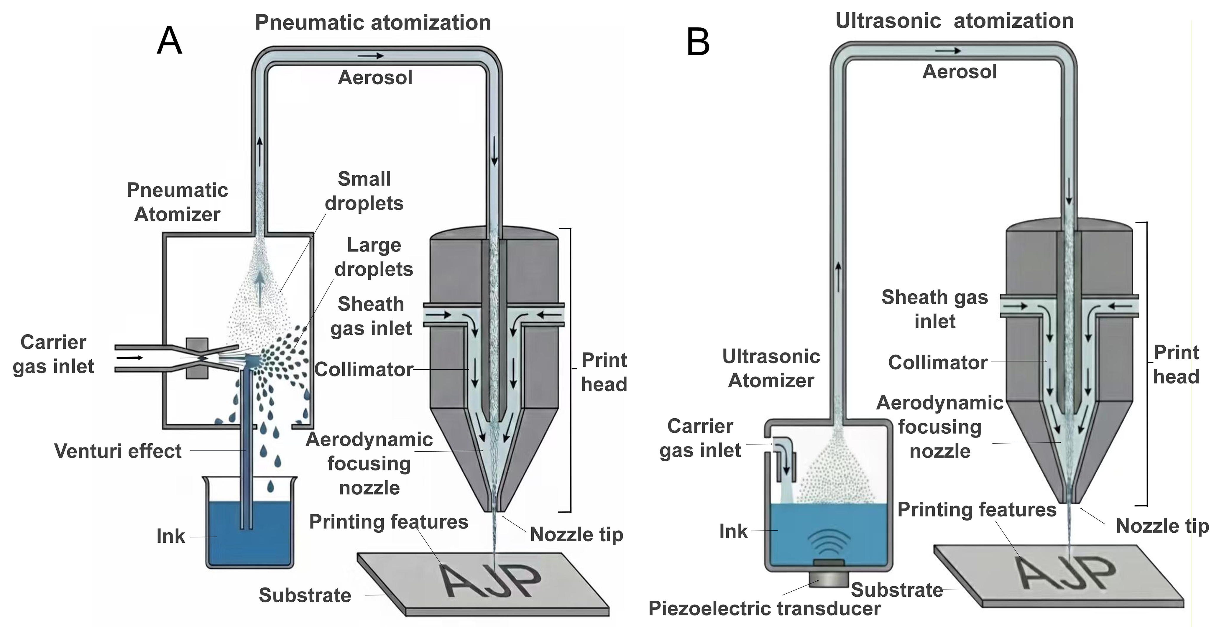
Figure 4. Schematic illustration of the working principle of AJP based on (A) Pneumatic atomization and (B) Ultrasonic atomization. AJP: Aerosol jet printing.
The AJP process can be divided into three key stages: ink atomization, aerodynamic focusing, and material deposition[53]. Although AJP enables high-precision printing, each stage involves specific process challenges and common defects.
The first step in AJP is ink atomization, which mainly relies on two mechanisms: pneumatic atomization[54] and ultrasonic atomization[55]. In pneumatic atomization, compressed gas flows through the atomizer nozzle to generate a high-velocity jet. According to the Venturi principle[56], this jet draws ink into the nozzle and breaks it into aerosol droplets. Larger droplets generated during atomization tend to collide with the atomizer walls and then return to the ink reservoir under the combined effects of carrier-gas inertia and gravity. In contrast, smaller droplets are carried by the carrier gas out of the atomization chamber for further processing. To reduce overspray caused by excessively small droplets, the aerosol generated by pneumatic atomization is usually passed through a microdroplet filter, commonly known as a virtual impactor (VI), to improve droplet size uniformity[57]. This filter operates via inertial separation within a laminar flow regime. Smaller droplets with insufficient inertia deviate from the main flow and are removed, whereas droplets within the target size range pass through the separation zone and are transported toward the printhead. Ultrasonic atomization utilizes a piezoelectric transducer immersed in a coupling medium (typically water) to generate acoustic waves through high-frequency oscillation. The acoustic waves propagate through the medium to a sample vial positioned above the transducer, where they form standing waves on the liquid surface[58]. The superposition of continuous acoustic waves produces pronounced wave crests, and the localized shear stress at these crests breaks the liquid into fine droplets. The resulting droplets are then entrained by an inert carrier gas to form a uniform aerosol, which is transported to the printhead for focusing and deposition[59]. However, both atomization methods exhibit inherent limitations. Ultrasonic atomization may heat the ink and potentially degrade functional materials, whereas pneumatic atomization often produces a broad droplet size distribution and shows reduced efficiency when processing high-viscosity inks.
The second step is the aerosol focusing. After atomization, aerosol droplets are transported by a carrier gas, typically nitrogen or air, from the atomization chamber to the printhead. Within the printhead, the carrier gas stream is enveloped by a coaxial high-velocity sheath gas. According to Bernoulli’s principle[60], the sheath gas creates a low-pressure region around the central flow, thereby confining the aerosol jet along the central axis of the nozzle. The primary objective of this stage is to convert the dispersed micron-sized droplets generated during atomization into a concentrated and stable jet, enabling micron-scale patterning on the substrate. The key challenge in this process is to achieve stable aerodynamic focusing[61], which requires precise and coordinated control of the carrier-gas and sheath-gas flow velocities[62].
The third step is ink deposition. When the focused aerosol jet reaches the substrate, it undergoes a series of dynamic processes, including impact, spreading, droplet coalescence, and solvent evaporation, and finally forms the printed pattern. Droplet behavior is governed by the combined effects of inertia, viscosity, surface tension, and substrate wettability. During continuous printing, poor coordination between droplet coalescence and solvent evaporation can cause defects such as coffee-ring effects, film nonuniformity, and void formation. To improve deposition uniformity and resolution, common process control strategies include regulating the substrate temperature, optimizing the printing path and layer-stacking strategy, and tailoring the solvent system[63-66]. Furthermore, for functional materials such as metallic nanoparticles and conductive polymers, post-deposition treatments, including thermal annealing, photonic sintering, and chemical post-processing, are often required to achieve structural densification and improve performance[67,68]. These treatments help the printed materials meet the electrical and mechanical reliability requirements of their intended applications.
In summary, AJP shows significant potential for high-quality fabrication, ranging from micron-scale interconnects to complex three-dimensional structures, and has attracted widespread research and industrial interest[69,70]. However, its further development and full manufacturing potential are still limited by several key process stages, including atomization, transport and focusing, and deposition/curing[71,72]. These limitations directly affect printing precision, structural uniformity, material compatibility, and production stability. Fundamentally, many of the current challenges in AJP arise from an insufficient systematic understanding of the multi-physics mechanisms involved in the process. Therefore, systematic and in-depth investigations of AJP technology, spanning both theoretical modeling and practical implementation, are essential for elucidating and overcoming its process bottlenecks. Accordingly, the following section focuses on optimization strategies and methods for addressing these challenges.
KEY TECHNOLOGY OPTIMIZATION METHODS FOR AJP
AJP offers notable advantages in terms of high resolution and material versatility. However, it continues to face a range of process-related challenges in progressing toward high-precision and high-reliability manufacturing. This section reviews current optimization approaches for addressing these challenges, with a focus on three key aspects: (1) control of the aerosol jet focusing process by printing parameters and additional physical fields; (2) regulation of ink morphology during deposition and curing; and (3) implementation strategies for conformal printing on flexible/complex curved surfaces.
Spraying and focusing: overcoming challenges in line width and morphology consistency
The uniformity of printed linewidth and edge morphology is critical for circuit performance. The primary challenges at this stage arise from instability in aerosol jet focusing, nonuniform ink droplet size distributions, and variations in droplet trajectories during flight. These issues are influenced by multiple factors, including atomizer parameters, ink properties, airflow conditions, nozzle geometry, printing pitch, and substrate characteristics[73].
Overspray, which appears as sparse, diffuse, mist-like deposits along the edges of printed traces, is a major process defect. It severely reduces print resolution and edge sharpness and may also cause electrical shorts. Pneumatic focusing has been widely used to reduce excessive spraying[74], However, the physical mechanisms of overspray and its quantitative prediction are still not fully understood. To address this issue, Chen et al. developed a three-dimensional computational fluid dynamics (CFD) model showing that the interaction between droplet size and sheath-gas velocity governs overspray formation and explains its non-monotonic dependence on flow velocity[71]. From a dimensionless perspective, the inertial response of droplets is typically characterized by the Stokes number (Stk). Small droplets with Stk << 1 are easily deflected by the airflow and become a major source of overspray[75]. Building on this work, Feng et al. proposed an image-based quantitative method to evaluate overspray based on area coverage. They showed that overspray generally scales with linewidth and can be suppressed by increasing the ejection velocity and optimizing gas-flow conditions[76]. The overall airflow regime is characterized by the Reynolds number (Re). Both excessively high and low Reynolds numbers can disrupt jet stability[55]. Accordingly, precise control of gas dynamics is critical: the sheath and carrier gas flow rates determine jet focusing and print quality[77], and their ratio, defined as the focusing ratio (FR), is widely used to regulate jet confinement[78]. However, changing only the FR is not sufficient for comprehensive and stable control of jet characteristics, Ramesh et al. incorporated total gas flow into a systematic analysis, showing that excessive flow broadens line width and must be coordinated with FR, while also revealing that submicron droplets tend to diffuse with the gas flow and contribute to overspray, whereas larger droplets (> 2 μm) are more effectively focused, enabling sharper features[79]. To address this limitation, Jin et al. developed a high-fidelity CFD model that links in-flight dynamics with post-impact behavior. Their results showed that near-substrate pressure fields can induce droplet splashing and satellite formation, thereby contributing to overspray[80].
In addition to improving mechanistic understanding through modeling, further improvement in printing precision requires attention to the microscopic phase changes of droplets during flight. Recent studies have shown that in-flight droplet evaporation is a key mechanism for overspray formation. Peripheral droplets can rapidly evaporate and shrink after contacting dry sheath gas. This process reduces their inertia, namely the Stk, and prevents them from effectively reaching the substrate, thereby causing overspray. Based on this mechanism, solvent-vapor presaturation of the sheath gas has been proposed to suppress droplet evaporation[81]. Experiments showed that this approach reduces overspray by approximately 70% for water-based polyimide (PI) inks and significantly improves line edge morphology [Figure 5A].
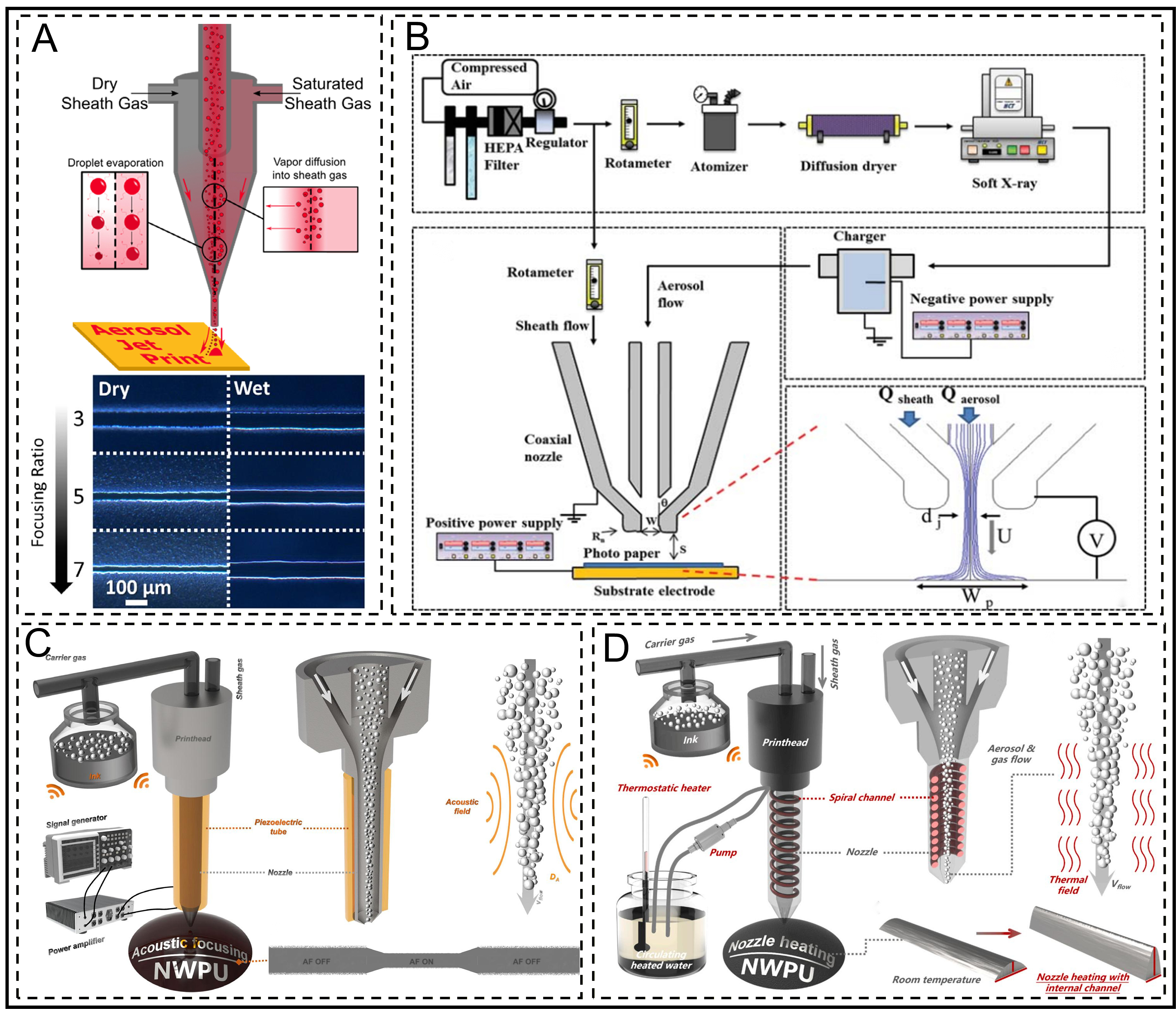
Figure 5. Spray and focusing optimization strategies. (A) Schematic of the AJP setup and process using dry sheath gas on the left and saturated sheath gas on the right, together with a comparison of the corresponding printing results[81]. Reprinted with permission[81]. Copyright 2025, Small Science; (B) Schematic and system diagram of focusing optimization using an electric field[82]. Reprinted with permission[82]. Copyright 2013, Aerosol Science and Technology; (C) Schematic and system diagram of acoustic-focusing-assisted AJP[39]. Reprinted with permission[39]. Copyright 2024, Nature Communications; (D) Schematic and system diagram of ring-shaped-thermal-field-assisted AJP[40]. Reprinted with permission[40]. Copyright 2025, Additive Manufacturing. AJP: Aerosol jet printing; HEPA: high efficiency particulate air.
To achieve more active and precise control of jet behavior and deposition morphology, researchers have introduced external physical fields to expand the process design space through multi-physics coupling. In the early practices, Park et al. demonstrated that applying an electric field inside a coaxial nozzle can combine aerodynamic and electrostatic forces. This method enables effective focusing and stable deposition of nanoparticles and microparticles, even under low-Stokes-number conditions[82]. This strategy significantly reduces the feature size of deposited patterns and improves deposition predictability [Figure 5B]. Building on this approach, more multi-physics field-assisted strategies have been explored in recent years. Among them, acoustic focusing has gradually attracted attention as a non-contact regulation method. Annular acoustic field focusing technology applies additional focusing forces to nanoparticles within the jet by introducing acoustic waves at specific frequencies. When combined with an improved nozzle structure, this method achieved ultrafine printing with linewidths below 6 μm and overspray below 0.1 μm. It also increased the line conductivity to 180% of that obtained without focusing[39], as shown in Figure 5C. In addition, a nozzle design with an internal heating channel has been reported. In this design, constant-temperature hot water circulates through a spiral flow channel inside the nozzle, forming a ring-shaped thermal field around the aerosol flow, as shown in Figure 5D. This thermal field significantly enhances aerodynamic focusing by regulating gas density and pressure distribution. As a result, it improves deposition morphology. The linewidth decreased from 14.78 to 7.02 μm, the thickness increased from 1.14 to 2.06 μm, and the aspect ratio improved to approximately 0.3. This optimization primarily stems from the thermal field’s regulatory effect on the convective flow. This method has been applied to fabricate high-density circuits with a line pitch of
Based on the above studies, CFD modeling and parameter optimization are easy to implement because they do not require hardware modification. However, their accuracy in describing complex multi-physics coupling remains limited. The solvent vapor saturation method can reduce over-spraying by approximately 70% and is particularly suitable for water-based inks. However, it requires an additional bubbling device. Electric-, acoustic-, and thermal-field-assisted approaches can achieve higher resolution (line width < 10 μm) and improved deposition morphology, but involve greater hardware integration complexity. Therefore, strategies for overcoming linewidth variation and morphological inconsistency have shifted from early empirical adjustment based on a single FR to more systematic approaches. These approaches include global gas-flow management, full-process simulation, in-flight phase-change control, and multi-physics assisted focusing. These advances have significantly improved the manufacturing accuracy and on-demand printing capability of AJP. However, single-nozzle systems still have low throughput, and scale-up production remains challenging because it is difficult to maintain consistency among multiple nozzles. Moreover, the trade-off between printing speed and resolution has not been sufficiently analyzed, and the long-term operational reliability of AJP still requires further investigation.
Morphology control and post-deposition processing: ensuring functional structure and performance
Jet optimization and precise deposition ensure accurate initial line formation. However, the spreading, drying, coalescence and final curing processes after droplet landing also directly determine the microstructure and macroscopic properties of the functional layer. In other words, jet formation and deposition control material placement, whereas post-processing determines whether the deposited materials can achieve the desired functional performance. Therefore, after aerosol jet optimization and precise deposition, as discussed in Section “Spraying and focusing: overcoming challenges in line width and morphology consistency”, the final shaping and curing of droplets on the substrate directly determine the core performance of functional devices. Key challenges at this stage include the coffee ring effect[83], high porosity, and poor microstructural compactness[84]. These defects can cause nonuniform resistance in conductive patterns, reduce overall conductivity, weaken mechanical strength and adhesion, and decrease pattern resolution and line definition. Consequently, they limit device performance and reliability. In optical applications, they may also cause nonuniform coating thickness or transparency and accelerate material aging. Therefore, active control of post-deposition morphology and effective post-processing are critical for ensuring that printed devices, such as electrodes, sensors, and energy storage components, achieve the expected performance and reliability.
To address these issues, morphological control and post-processing strategies usually focus on two stages: regulating the aerosol state and deposition rate, and optimizing the microstructure and intrinsic properties of the deposited material. The first stage involves regulating the “wet/dry state” during aerosol deposition to influence the diffusion and curing rates. As discussed at the end of Section “Spraying and focusing: overcoming challenges in line width and morphology consistency”, presaturating the sheath gas with solvent vapor during jetting can control droplet evaporation and thereby regulate the physical state of droplets, including viscosity and surface tension, when they contact the substrate[81,85]. This process directly affects ink spreading, polymerization, and solvent evaporation after deposition, and it serves as an important upstream method for improving deposition morphology. The second stage is to conduct active intervention after droplet deposition, with the focus on precisely controlling the energy input to optimize the physical morphology and functional properties of the deposited ink. The most traditional and direct method is substrate heating, which regulates droplet spreading, wetting, and drying rates. Under appropriate conditions, substrate heating promotes rapid solvent evaporation and suppresses the coffee-ring effect. Winnicki et al. demonstrated that online heating of PI substrates to 90 °C during AJP printing significantly accelerated solvent evaporation in silver nanoparticle (AgNP) ink, facilitating rapid particle aggregation and solidification post-deposition[84]. This method effectively suppressed the coffee-ring effect and excessive spreading. It reduced the linewidth from 31 to 19 µm, increased the thickness from 1.2 to 5.5 µm, and improved structural density and electrical reliability. In contrast, Zhou et al. employed substrate heating not primarily for linewidth reduction or edge definition, but as a strategy for structural regulation during deposition[68]. By tuning substrate temperature, they controlled solvent evaporation and particle mobility, thereby governing nanoparticle assembly behavior. This enabled the transition from dense films to loose hierarchical architectures and provided a route for fabricating three-dimensional micro/nanostructures with enhanced functional performance, as shown in Figure 6A. Substrate heating mainly optimizes the macroscopic morphology of the film. However, for functional inks, especially conductive inks containing metallic nanoparticles, better intrinsic electrical and mechanical properties usually require an additional processing step, namely sintering or curing. Furthermore, technologies such as electro-sintering[86] and microwave sintering[87] have been extensively studied and verified, offering diverse post-processing options for different material systems and application scenarios.
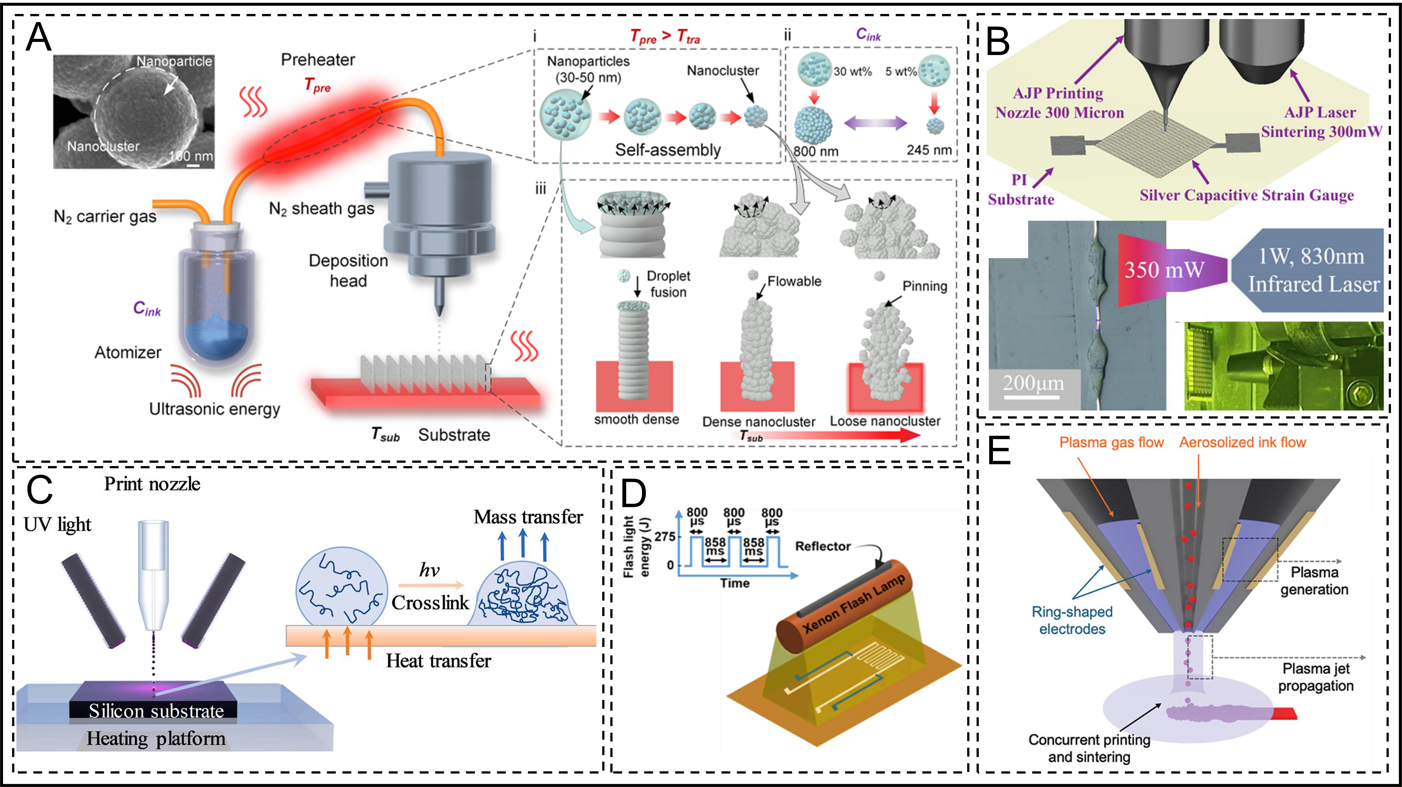
Figure 6. Morphological control and post-deposition processing optimization strategies. (A) Schematic of the AJP system consisting of an ultrasonic atomizer, preheater, movable deposition head, and substrate[68]. Reprinted with permission[68]. Copyright 2025, ACS Nano; (B) Schematic diagram of the laser-assisted sintering AJP process[41]. Reprinted with permission[41]. Copyright 2024, The International Journal of Advanced Manufacturing Technology; (C) Schematic of the in situ photopolymerization of microdroplets after deposition in the AJ printing process[42]. Reprinted with permission[42]. Copyright 2023, Additive Manufacturing; (D) Schematic diagram of the intense pulsed light sintering process for AJP-printed films[67]. Reprinted with permission[67]. Copyright 2025, ACS Applied Electronic Materials; (E) Schematic of aerosol and plasma co-jet printing for concurrent ink deposition and sintering[91]. Reprinted with permission[91]. Copyright 2025, Small. AJP: Aerosol jet printing; PI: polyimide; UV: ultraviolet.
Nevertheless, conventional thermal sintering often requires high temperatures that exceed the thermal tolerance of flexible polymer substrates, which limits its application in flexible electronics. To address this challenge, alternative sintering strategies compatible with temperature-sensitive substrates have been developed. Among them, photonic sintering uses selective light absorption to induce localized high-temperature sintering while keeping the overall substrate temperature low. Therefore, it is particularly suitable for flexible electronic applications. For instance, laser sintering enables precise control over the spatiotemporal distribution of energy, making it suitable for thermosensitive substrates. Wei et al. used AJP to deposit AgNP ink, Metalon JS-A426, on PI and polyethylene terephthalate (PET) substrates to fabricate a bilayer capacitive strain sensor[41]. In this work, laser sintering (stable process parameters: 350 mW) was applied to the PI substrate. This process enabled selective melting of AgNPs and the formation of dense electrodes (~10 μm thick) without damaging the substrate, resulting in high conductivity, strong adhesion, and stable electrical performance [Figure 6B]. Beyond laser sintering, other mature photopolymerization/sintering methods include photonic sintering, as well as ultraviolet (UV) lamp sintering, infrared lamp sintering[88,89], and flash lamp sintering[90]. Among these methods, real-time UV processing is particularly suitable for polymer inks containing photoinitiators because it enables rapid in situ photopolymerization and curing. Li et al. integrated UV LEDs onto the side of the printhead to enable simultaneous illumination and printing[42]. This method immediately fixed the printed patterns, effectively prevented excessive spreading of low-viscosity materials, and enabled the printing of microcolumn arrays with linewidths of 30 µm and heights greater than 150 µm, as shown in Figure 6C. In addition, the more mature photonic flash sintering method enables instantaneous and selective sintering of nanoparticle inks through millisecond-scale light pulses, making it suitable for fabricating high-performance electronic devices on low-melting-point flexible substrates. For example, AJP was used to deposit gold nanoparticle and indium tin oxide (ITO) nanoparticle inks onto PI substrates[67]. By optimizing the intense pulsed light sintering parameters, the sintering process was completed in less than two seconds, resulting in dense and conductive networks of gold and ITO nanoparticles, as shown in Figure 6D. After flash sintering, the sensors exhibit excellent stability at temperatures up to 350 °C, while maintaining nearly unchanged performance even after 500 bending and torsion cycles. This approach provides a new pathway for the rapid and reliable fabrication of high-temperature-resistant flexible multimodal sensors.
In addition, plasma sintering has been preliminarily studied to minimize substrate damage. Du et al. coupled AJP with an atmospheric-pressure non-thermal plasma jet, enabling room-temperature in situ sintering of metal nanoparticle inks during the deposition process[91], as shown in Figure 6E. By synchronizing deposition and sintering, this approach eliminates the need for conventional post-processing and significantly reduces the overall fabrication time. Moreover, the coupled printing strategy demonstrates excellent substrate compatibility, allowing for the direct fabrication of functional devices on a wide range of temperature-sensitive materials, including biological substrates. Finally, reactive precursor inks suitable for AJP have recently been developed to avoid the effect of additional energy fields on flexible or curved substrates. These inks undergo chemical reactions during or after the printing process[92,93]. Because this approach does not rely on nanoparticle-based inks, it can significantly reduce or completely eliminate the sintering requirements after deposition, further minimizing the damage to the flexible substrate.
Compared with the above post-processing methods, the substrate heating is simple but has a limited temperature range (< 150 °C). Laser sintering offers good spatial selectivity but has low efficiency for large-area processing. Intense pulsed light sintering is extremely fast, with processing times at the millisecond scale, and is suitable for roll-to-roll manufacturing. However, it strongly depends on the optical absorption properties of the ink. Plasma sintering can achieve in situ processing at room temperature and is compatible with biological substrates, but the equipment is complex. Reactive precursor inks can avoid thermal damage, but their conductivity is usually lower than that of sintered nanoparticle films. Therefore, in flexible electronics manufacturing, the choice of post-processing method should be determined based on the thermal tolerance of the substrate, conductivity requirements, and production efficiency. Overall, post-deposition processing has evolved from simple substrate heating to more precise energy-management strategies. These strategies include controlling heat transfer during deposition, achieving rapid and selective sintering or curing with tailored photon energy, using low-temperature plasma sintering for thermally or energetically sensitive substrates such as biological materials, and developing reactive precursor inks that reduce or eliminate post-treatment. The core principle is precise spatial and temporal control of energy input. This strategy enables defect mitigation, morphological optimization, functional performance enhancement, and preservation of flexible substrate integrity.
Conformal printing for flexible and complex surfaces: path, platform, and design optimization
As flexible electronics evolve toward wearable, stretchable, and conformal integrated systems, especially for devices deployed on complex three-dimensional surfaces, the related printing challenges have become increasingly important. For flexible and stretchable substrates, the main challenges include maintaining electrical stability under repeated mechanical deformation, suppressing crack formation caused by stress concentration, and achieving uniform deposition on dynamically changing geometries. Flexible conductive lines fabricated by AJP can maintain stable electrical performance under repeated bending, showing clear advantages for addressing these challenges. Luo et al. fabricated MXene/poly(3,4-ethylenedioxythiophene):poly(styrenesulfonate) (PEDOT:PSS) flexible micro-capacitors on both planar and curved fiber surfaces, thereby improving the stability of flexible electronic devices[94]. In addition, the high resolution and mask-less nature of AJP enable the rapid fabrication of complex patterns. Xu et al. printed various strain-adaptive structures, such as serpentine and wavy geometries, for flexible electronic devices[95] [Figure 7A]. The resulting strain sensors showed a wide sensing range of up to 660%, providing a systematic strategy for structural optimization in flexible and stretchable electronic devices. These structural designs effectively redistribute mechanical strain and reduce the risk of failure, thereby improving the durability and performance of stretchable electronic systems on complex curved surfaces.
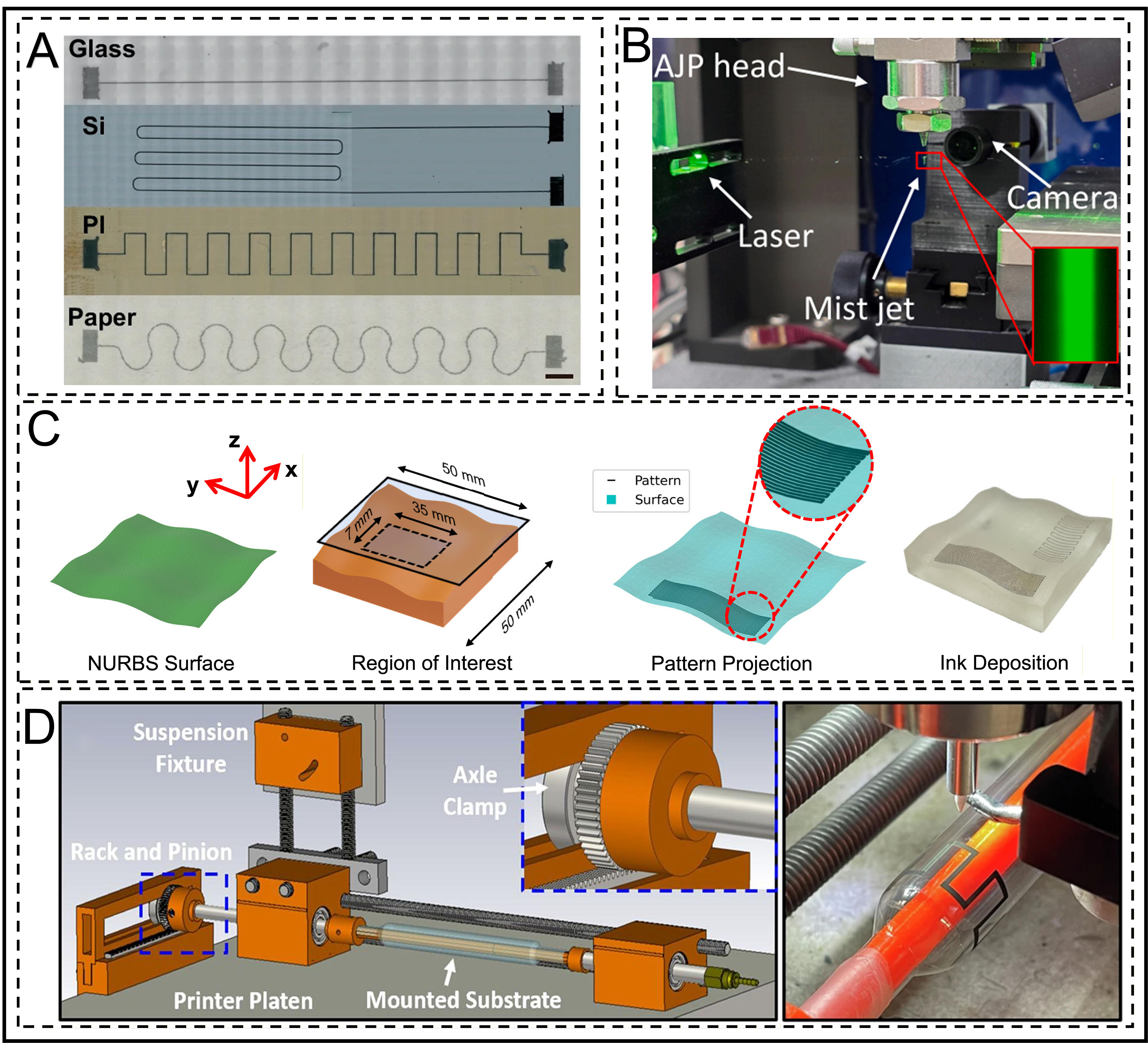
Figure 7. Conformal printing strategies for flexible, stretchable, and complex surfaces. (A) AJP of patterns on various substrates[95]. Reprinted with permission[95]. Copyright 2025, Nature Communications; (B) AJP system equipped with a visualization unit, where camera and laser are oriented perpendicular to each other[73]. Reprinted with permission[73]. Copyright 2024, Journal of Manufacturing Processes; (C) AJP on topologically optimized complex curved surfaces[43]. Reprinted with permission[43]. Copyright 2024, Journal of Manufacturing Processes; (D) AJP system integrated into a turning lathe for curved-surface printing[44]. Reprinted with permission[44]. Copyright 2024, npj Flexible Electronics. AJP: Aerosol jet printing; PI: polyimide; NURBS: non-uniform rational B-splines.
When AJP is applied to complex three-dimensional surfaces, the nozzle often operates at a larger stand-off distance from the substrate and is difficult to keep perpendicular to the local surface. This condition can cause tilted deposition and disrupt jet symmetry, resulting in asymmetric line cross-sections, increased linewidth, blurred edges, and reduced conductivity[38]. Under these conditions, printing quality is governed not only by material properties and process parameters but also, more critically, by the dynamic geometric relationship between the nozzle and the substrate. To address this issue, Mosa et al. developed a laser-scattering-based jet visualization method for real-time observation and analysis of spray morphology and dynamic behavior during AJP[73], as shown in Figure 7B. By measuring the spray diameter and penetration length, this method clarifies how parameters such as spray velocity and sheath-gas flow rate affect jet focusing and stability. This approach extends the working distance to more than 10 mm and enables high-quality printing on complex three-dimensional surfaces. It also provides an effective visualization tool and theoretical basis for real-time monitoring, parameter optimization, and precise remote printing in AJP. For path planning, the core challenge is to accurately, continuously, and adaptively map two-dimensional printing paths onto three-dimensional surfaces. Traditional approaches usually triangulate CAD models before generating printing paths, which often introduces geometric approximation errors and path discontinuities. To address this problem, Jignasu et al. proposed a direct path planning method based on non-uniform rational B-splines (NURBS) parametrized surfaces[43]. This method bypasses the triangulation step and directly uses the high-precision mathematical representation of CAD models. As a result, it generates smooth and continuous printing trajectories that strictly conform to the surface geometry, as shown in Figure 7C. Compared with previous mesh-based approaches[96], this strategy significantly enhances geometric fidelity and trajectory continuity. It also maintains a constant nozzle-to-surface distance and avoids collisions. These advantages represent important progress toward higher digitalization and automation in conformal path generation.
Precise trajectory planning alone is insufficient. The hardware motion system must also be able to implement the planned trajectory. For specific surface types, such as rotationally symmetric bodies, customized motion platforms can simplify the printing process and improve print quality. One study integrated a lathe-type rotating attachment into a three-axis AJP system and extended it into a lathe-type aerosol jet printing (LAJ) platform with cylindrical-coordinate motion capability[44], as shown in Figure 7D. Through coordinated substrate rotation and nozzle translation, the system maintains the nozzle perpendicular to the printing surface, thereby reducing defects induced by tilted deposition. This enables uniform, high-resolution conformal circuit printing on flexible films, medical catheter balloons, conical surfaces, and other stretchable curved substrates. The study demonstrates the feasibility of extending AJP from planar printing to three-dimensional conformal integration in flexible electronics, although further experimental validation is still required. It also highlights the importance of application-specific hardware optimization for the reliable fabrication of high-performance devices.
In summary, extending AJP from planar substrates to flexible, stretchable, and complex three-dimensional surfaces introduces new challenges, including mechanical reliability, strain adaptability, and geometry-dependent deposition behavior. At present, AJP still has inherent limitations in printing on complex curved surfaces. Path planning mainly relies on offline programming and lacks real-time deformation feedback, which limits its applicability to dynamically deforming substrates. Addressing these challenges requires a shift from isolated process optimization to an integrated strategy that combines structural design, adaptive path planning, and advanced motion control. This strategy can enable high-fidelity and mechanically robust conformal printing on diverse substrates. It also supports the reliable fabrication of flexible and stretchable electronic devices and provides a basis for large-scale conformal manufacturing on complex three-dimensional surfaces. This section establishes the physical constraints and process guidelines for subsequent material design and ink-formulation optimization, thereby providing a basis for the discussion of material printability and performance control in Section “AJP MATERIALS”.
AJP MATERIALS
AJP processability
In AJP, processability depends on the interactions among ink formulation, aerosol generation, transport, focusing, and deposition. The ink serves as the aerosol source, and its key physicochemical properties, including viscosity, surface tension, solvent volatility, particle size, and solid loading, directly affect aerosol atomization efficiency, aerosol stability, and printing accuracy[97,98]. Although AJP is generally considered to have broad material compatibility, its practical processing window is still limited by ink-related properties. Therefore, precise control of ink formulation is essential for achieving repeatable and high-quality printing. This section summarizes how the physicochemical properties of AJP inks affect key process steps, including atomization, transport, focusing, and deposition. It also summarizes the recommended parameter ranges for two different atomization mechanisms, providing guidance for the preparation of functional inks suitable for high-quality AJP.
Viscosity and rheology
Viscosity primarily controls atomization. Ultrasonic atomizers require low-viscosity inks (typically < 10-12 cP) to generate stable aerosols with narrow droplet size distributions[99,100]. Pneumatic atomizers can tolerate much higher viscosities, up to approximately 1,000 cP. However, they generally produce broader droplet size distributions and less stable aerosols[98,101].
Surface tension
Surface tension, together with viscosity, regulates droplets spheroidization and aerosol formation. Although predictive criteria similar to the inkjet Z number are still lacking for AJP, excessively low or high surface tension can reduce atomization efficiency, promote overspray, or lead to poor feature definition. Surface tension also strongly affects ink wetting and spreading on the substrate[102,103].
Solvent vapor pressure
Solvent volatility determines droplet evaporation during aerosol transport. Highly volatile solvents may cause premature drying and overspray, whereas low-volatility solvents can improve aerosol stability but may lead to excessive spreading or incomplete consolidation. Solvents with boiling points around 180 °C, often used in multicomponent solvent systems, are commonly selected to balance these effects[104,105].
Particle size and loading
Particles should be sufficiently small (typically < 1 µm) to avoid clogging and ensure stable aerosolization. A narrow particle size distribution is also essential because atomization preferentially entrains smaller particles. A broad particle size distribution can cause time-dependent variations in printed material composition during prolonged operation[71].
Based on the above discussion of the physicochemical properties of AJP inks, the recommended ranges of key ink parameters for different atomization methods are summarized in Table 2.
Recommended ranges of viscosity, particle size, solid loading, and solvent type for different atomization methods
AJP of functional materials
AJP is widely regarded as one of the most versatile direct-write additive manufacturing techniques because it can deposit a broad range of functional materials with micrometer-scale precision. In principle, any material that can be formulated into a stable and jettable ink that meets the atomization requirements discussed in Section “AJP processability” can be processed by AJP. This capability has established AJP as an important manufacturing platform for printed and flexible electronics, sensors, energy storage devices, and bio-integrated devices. In this section, the state of the art of AJP is reviewed according to the functional roles of the printed materials, with a focus on conductive materials, semiconductors, dielectrics and biological materials. For each material class, representative ink formulations, processing strategies, and device-level demonstrations are discussed. The discussion highlights both the opportunities enabled by AJP and the material-specific challenges that still limit its wider technological adoption.
Conductive materials
Conductive inks represent the most mature and extensively studied class of materials processed by AJP, reflecting the central role of this technique in printed electronics and interconnect fabrication. Because AJP can transport and aerodynamically focus fine aerosol streams, it enables the deposition of conductive materials on a wide range of substrates, including flexible, rough, and nonplanar surfaces. It also supports both planar and three-dimensional architectures. Based on ink formulation and conduction mechanism, conductive AJP inks can be broadly classified into metal-based, carbon-based, polymer-based and metal-organic decomposition (MOD) systems.
Among conductive ink systems for AJP, metal-based inks, especially metallic nanoparticle inks, dominate the current literature. AgNP inks have been the most widely studied because of their high conductivity, chemical stability, and mature sintering strategies. Efimov et al. showed that substrate heating during multilayer AJP reduced ink spreading and enabled the fabrication of silver lines with high aspect ratios and resistivities
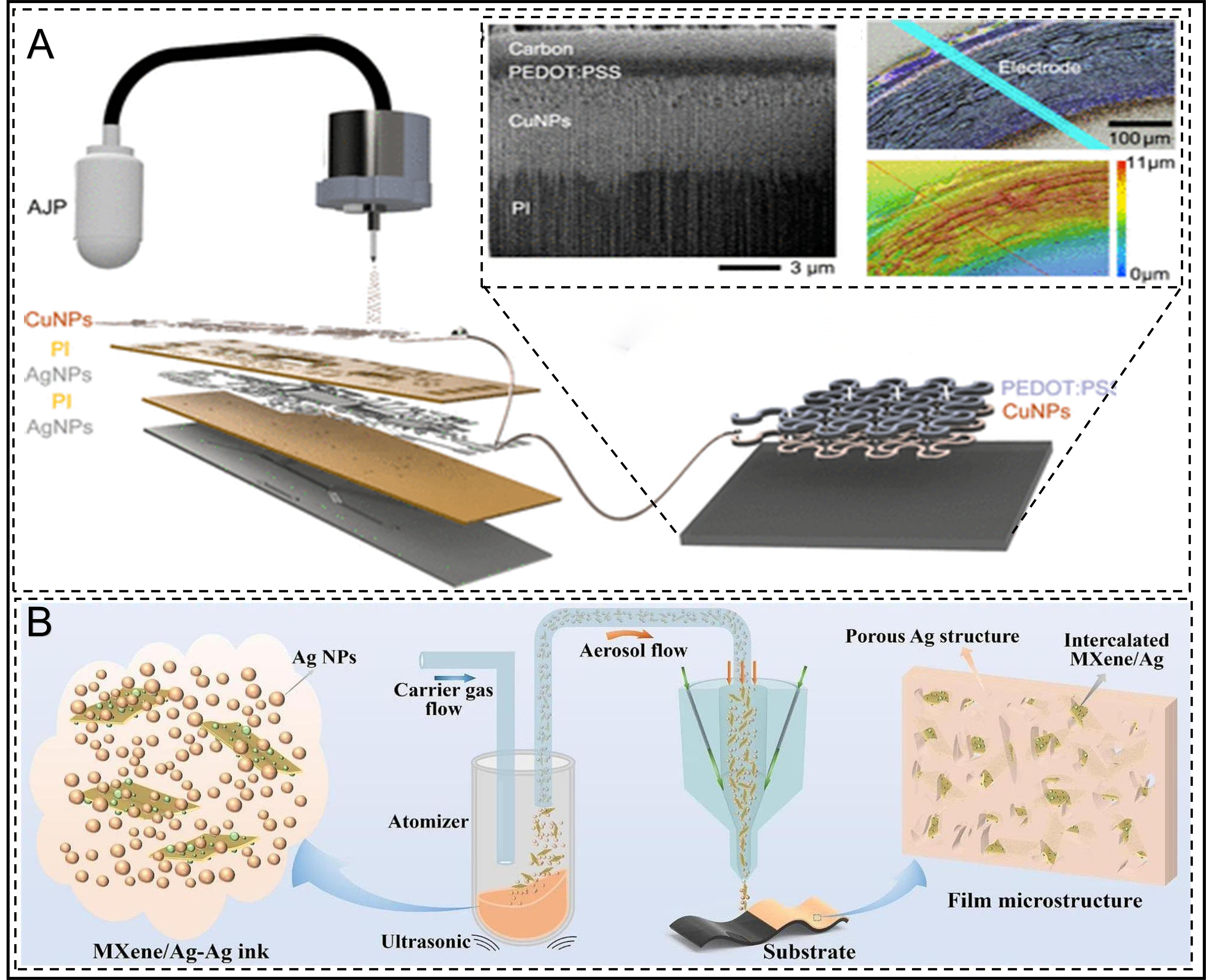
Figure 8. Metal-based and carbon-based aerosol jet inks. (A) AJP-based fabrication of integrated electronics using PI, AgNPs, CuNPs, and PEDOT:PSS for a multilayer circuit and electrode, together with sequential photographs showing the circuit-printing process using five layers and three materials[108]. Reprinted with permission[108]. Copyright 2024, ACS Applied Materials & Interfaces; (B) Schematic diagram of the AJP process using the MXene/Ag-Ag composite ink[114]. Reprinted with permission[114]. Copyright 2025, Chemical Engineering Journal. AJP: Aerosol jet printing; PI: polyimide; AgNPs: silver nanoparticles; CuNPs: copper nanoparticles; PEDOT:PSS: poly(3,4-ethylenedioxythiophene):poly(styrenesulfonate).
To make AJP suitable for flexible and bio-integrated electronic devices, conductive polymers have also become an important material category. Representative examples include PEDOT:PSS, polyaniline (PANI), and polypyrrole (PPy). Among them, PEDOT:PSS has been widely printed as flexible electrodes and interconnects, yielding uniform, continuous films with electrical performance competitive with spin coating and inkjet printing[120,121]. Luo et al. used PEDOT:PSS as a bridge to connect the folded spherical Ti3C2Tx structure [Figure 9A], while enhancing both the electronic conductivity of the printed electrode and its bending stability[94]. PANI-based inks have been used to fabricate highly sensitive NH3 sensors entirely by AJP[122]. Although polymer conductors generally exhibit lower intrinsic conductivity than metallic systems, their solution processability, mechanical robustness and biocompatibility make them particularly attractive for applications where flexibility and functional integration are required. Finally, MOD inks have emerged as a powerful alternative to nanoparticle-based formulations. MOD inks consist of metal ions coordinated with organic ligands in true molecular solutions. Therefore, they avoid particle agglomeration and sedimentation and reduce the need for residual surfactants, which can otherwise limit electrical performance[123]. Existing studies have shown that MOD inks can generate dense metal films with conductivities close to bulk values through thermal decomposition or plasma-assisted decomposition, often at relatively low processing temperatures[124]. Ag-based[93,125] and Pd-Ag-based[126] MOD inks have been reported to be fully compatible with AJP, enabling high-resolution printing and excellent electrical performance even on temperature-sensitive substrates, as shown in Figure 9B. Therefore, MOD inks bridge the gap between conventional nanoparticle systems and next-generation solution-processed metals, further demonstrating the versatility of AJP as a platform for high-performance printed conductors.
Figure 9. Conductive-polymer and MOD aerosol jet inks. (A) The composite ink of PEDOT:PSS/Ti3C2Tx composite ink used for supercapacitor fabrication on the surface of flexible fibers by AJP[94]. Reprinted with permission[94]. Copyright 2025, Advanced Engineering Materials; (B) Printing results from the first to fifth passes using Pd-Ag MOD ink and the corresponding single-metal inks, together with secondary electron images and scanning electron microscopy images[126]. Reprinted with permission[126]. Copyright 2024, Advanced Science. MOD: Metal-organic decomposition; PEDOT:PSS: poly(3,4-ethylenedioxythiophene):poly(styrenesulfonate); AJP: aerosol jet printing; TPU: thermoplastic polyurethane.
Semiconductor materials
Despite the growing interest in printed and flexible electronics, the use of AJP for oxide and perovskite semiconductors remains relatively limited but highly promising. Early studies have demonstrated its potential for fabricating photodetectors, thin-film transistors, and other active devices. AJP also provides a platform for exploring hybrid architectures by combining different classes of semiconductors or integrating them with conductive two-dimensional materials. These capabilities highlight its promise for next-generation printed and flexible electronics. Metal oxide semiconductors represent the most established class of AJP-printed semiconductors. Zinc oxide (ZnO), in particular, has been widely adopted because of its solution processability, environmental stability and compatibility with low-temperature processing. AJP of ZnO nanoparticle inks has enabled the fabrication of UV photodetectors on flexible substrates [Figure 10A]. In these devices, the inherently porous morphology of aerosol-deposited films enhances light absorption and surface-related photoresponse[127]. Beyond photodetection, AJP has also been used to deposit ZnO as the active semiconductor layer in thin-film transistors, demonstrating that aerosol-based printing can be extended beyond passive components to functional electronic devices[128,129]. These studies collectively show that AJP is suitable for oxide semiconductors that tolerate moderate thermal treatment and benefit from nanostructured film morphologies. Perovskite semiconductors have recently emerged as a highly promising but still relatively underexplored class of materials for AJP. Their high absorption coefficients, long carrier diffusion lengths, and solution processability make them attractive candidates for printed optoelectronic devices. A notable example is the AJP of three-dimensional methylammonium lead iodide (MAPbI3) perovskite architectures for X-ray photodetectors. These devices exhibited record sensitivity and clearly demonstrated the ability of AJP to fabricate thick, vertically structured semiconductor features with micrometer-scale precision[130]. This work highlights a distinctive advantage of AJP over planar printing methods, namely the possibility to directly build three-dimensional semiconductor geometries that enhance device performance. Organic and hybrid semiconductors further expand the application scope of AJP, particularly for low-voltage and flexible electronics. In addition, AJP has been used to print dielectric and semiconductor layers directly onto prefabricated semiconductor chips without degrading device performance, demonstrating its compatibility with hybrid integration schemes and advanced packaging applications[131,132]. Overall, although the range of semiconductor materials processed by AJP is currently narrower than that of conductive inks, existing studies clearly demonstrate the feasibility of printing functional semiconductor layers and complete active devices. Key challenges remain in film uniformity, defect control, and post-deposition treatment on flexible substrates. These factors are critical for improving device-to-device repeatability and operational lifetime.
Figure 10. Semiconductor and biological aerosol jet inks. (A) Photodetector fabricated by AJP using ZnO semiconductor ink[127]. Reprinted with permission[127]. Copyright 2018, ACS Photonics; (B) AJP of SU-8 to cover silver traces[132]. Reprinted with permission[132]. Copyright 2022, J Electron Mater; (C) AJP of Cy5-streptavidin onto a substrate to form an affinity interface with silver nanowires[136]. Reprinted with permission[136]. Copyright 2020, Biofabrication. AJP: Aerosol jet printing; ZnO: zinc oxide.
Dielectric materials
Dielectric materials represent a critical class of functional inks for AJP because they enable the fabrication of insulating layers, passivation coatings, gate dielectrics, and three-dimensional dielectric architectures in printed electronic systems. Unlike conductive or semiconducting inks, dielectric formulations must simultaneously provide high electrical resistivity, low leakage current, smooth film morphology, and strong adhesion. Polymeric dielectrics are the most widely used materials in this context because of their solution processability and mechanical compliance. Epoxy-based photoresists, such as SU-8, are representative examples because they enable high-resolution patterning and good chemical stability. AJP of SU-8 has been demonstrated for conformal passivation and encapsulation layers, as shown in Figure 10B. These printed films provide effective ionic isolation and environmental protection for the underlying conductive features[132], as shown in Figure 10B. Beyond conventional dielectrics, AJP offers unique advantages for patterning functional polymeric and hybrid insulating materials in advanced microfabrication processes. Several studies have used AJP to selectively deposit adhesive dielectric polymers, such as benzocyclobutene and water-based ethylene-vinyl acetate, for wafer bonding applications[133,134]. In these cases, the ability to locally define adhesive regions enables optimized bonding interfaces and improved process flexibility, which are difficult to achieve using traditional spin-coated films. Recent studies have also demonstrated the use of UV-curable and arylepoxy photopolymers to build free-standing three-dimensional dielectric microstructures by AJP. In these processes, in-flight or in situ crosslinking is used to stabilize multilayer vertical structures[135]. Overall, these results indicate that dielectric materials are particularly suitable for AJP when spatial selectivity, conformality, and three-dimensional structuring are required. Although challenges remain in achieving ultralow leakage and defect-free films over large areas, AJP provides a versatile platform for integrating dielectric layers into complex printed and flexible electronic systems. This capability complements its established role in conductive and semiconducting material processing.
Biological materials
AJP has emerged as a promising technique for printing biological and biofunctional materials, enabling applications in biosensing, bio-interfaces, and emerging bioelectronic systems[136]. Several studies have shown that AJP can process protein-based and biomolecular inks while preserving bioactivity. These inks can also be printed alongside conductive nanomaterial inks, such as silver nanowires, without cross-contamination or loss of functionality, as shown in Figure 10C. This multi-material capability, combined with the high spatial precision of AJP, highlights its potential for fabricating integrated bioelectronic and diagnostic devices, in which biological recognition layers must be accurately aligned with electronic transducers[31]. Beyond biosensing, AJP has been explored for bio-interfaces and tissue-interacting systems, where controlled material placement at the microscale is essential. Recent work has highlighted the use of AJP to deposit biocompatible and bio-functional coatings that promote selective cell adhesion and interaction, supporting applications in bio-integrated and bioelectronic devices[24]. In this context, AJP bridges the gap between high-resolution microfabrication techniques, which often lack material versatility, and bioprinting methods, which are typically limited in resolution.
To provide a clearer comparison of the optimization strategies discussed in Section “KEY TECHNOLOGY OPTIMIZATION METHODS FOR AJP” and the broad range of processable materials discussed in Section “AJP MATERIALS”, Table 3 summarizes representative AJP studies. Key parameters, including minimum feature size, electrical performance, material system, and processing strategy, are compared to highlight the trade-offs among resolution, conductivity, and process complexity in AJP. In summary, AJP functional inks still face challenges related to long-term storage stability, batch-to-batch consistency, and nozzle clogging caused by solvent evaporation. These issues adversely affect process repeatability and long-term device reliability. Therefore, current ink systems require further optimization for industrial applications.
Benchmark comparison of representative AJP studies, including key performance metrics such as minimum feature size, electrical properties, material systems, and processing strategies
| Material | Atomization | Min. linewidth (µm) | Conductivity/resistivity | Post-processing | Key strategy | Notes |
| AgNPs | Pneumatic | < 6 | 9.5 × 10⁶ S·m-1 | Not specified | Acoustic focusing | Ultra-fine focusing, reduced overspray[39] |
| AgNPs | Pneumatic | ~7 | 6 × 10⁶ S·m-1 | Thermal field-assisted | Thermal focusing | Improved aspect ratio[40] |
| AgNPs | Pneumatic | ~10 | Not specified | Laser sintering | Localized sintering | Compatible with flexible substrates[41] |
| AgNPs | Pneumatic | ~90 | 3 µΩ·cm | Thermal | Multi-layer heating | High aspect ratio lines[64] |
| AuNPs | Ultrasonic | ~60 | 1.9 × 10⁷ S·m-1 | Photonic flash sintering | Millisecond sintering | Stable up to 350 °C[67] |
| ITO NPs | Ultrasonic | ~60 | 1.5 × 10² S·m-1 | Photonic flash sintering | Millisecond sintering | Stable up to 350 °C[67] |
| ITO NPs | Pneumatic | Film (not lines) | 23.20 Ω·m-2 | Thermal annealing | Co-solvent ink | Transparent electrodes[137] |
| CuNPs | Pneumatic/ultrasonic | Not specified | 11.7 µΩ·cm | Photonic sintering | Encapsulation | Oxidation mitigation[108] |
| Ti3C2Tx/PEDOT:PSS | Ultrasonic | ~50 | Not specified | None | Hybrid ink design | Flexible devices[94] |
AJP APPLICATIONS
Printed and flexible electronics
Printed and flexible electronics constitute one of the most mature and industrially relevant domains for AJP, largely due to the demand for lightweight, thin, and mechanically compliant electronic systems. Unlike conventional microfabrication, which is often limited to planar substrates and subtractive patterning, printed electronics relies on the additive deposition of functional materials and supports a broader range of substrate chemistries and geometries. As a result, direct-write printing techniques can fabricate functional structures on substrates such as PET, PI, thermoplastic polyurethane, and other elastomers, allowing electronic systems to maintain performance under bending, twisting, or stretching[138]. Within this field, AJP occupies a distinctive position. It enables mask-less, high-resolution patterning while maintaining compatibility with conductive, semiconducting, and dielectric inks over a wide viscosity range. A key strength of AJP is its ability to form high-resolution conductive traces and interconnects, typically in the 10-50 µm linewidth range, with precise placement enabled by the sheath-gas focusing mechanism. This capability allows AJP to bridge the gap between inkjet printing, which is limited in resolution and surface conformity, and photolithography, which requires rigid substrates and multistep processing. As a result, AJP has been widely used in applications such as antennas, sensors, transparent electrodes, and conformal circuit routing. With appropriate sintering strategies, AJP-printed metallic traces can achieve conductivities close to bulk values. Combined with the ability to deposit materials on nonplanar or irregular surfaces, this feature makes AJP particularly suitable for heterogeneous integration and advanced packaging, where interconnects must reliably link components with different geometries or orientations[139,140].
Given the promising results achieved in conductive trace fabrication, the increasing use of AJP-printed electronics, especially on flexible substrates, is expected[141-143]. In emerging applications such as wearable sensors, epidermal electronic devices, soft robots, smart packaging, and foldable consumer devices, AJP can maintain high spatial resolution even when the substrate is deformed. This provides an important advantage over traditional microfabrication processes, which are mainly optimized for rigid silicon wafers. The broad material compatibility of AJP further supports this advantage because it enables the printing of dielectric materials and facilitates the integration of complete electronic architectures[144,145]. A major area in which the capabilities of AJP have been extensively leveraged is the fabrication of flexible antennas and radio-frequency identification (RFID) tags. In these devices, electrical performance depends not only on the conductivity of the printed traces but also on the geometric precision, surface uniformity, and substrate conformity of the patterned conductors. These requirements align well with the intrinsic strengths of AJP, and recent developments have expanded its relevance to higher-frequency operation. Flexible RF components are particularly attractive for conformal wireless systems, where antennas must operate reliably even when bent or wrapped around curved surfaces. The ability of AJP to maintain geometric precision on flexible substrates helps ensure stable impedance matching and predictable electromagnetic responses under mechanical deformation. Several studies have demonstrated that AJP can reliably produce fine conductive patterns suitable for ultrahigh-frequency, microwave, and emerging millimeter-wave applications[146-150]. AJP has also been used to fabricate terahertz (THz) metasurfaces on flexible substrates. As shown in Figure 11A, Ghosh
Figure 11. Applications of AJP in flexible electronics, sensors, and actuators. (A) Frequency-selective metasurfaces fabricated by AJP[45]. Reprinted with permission[45]. Copyright 2025, IEEE Transactions on Components, Packaging and Manufacturing Technology; (B) ITO-film transparent heaters fabricated by AJP[137]. Reprinted with permission[137]. Copyright 2024, Chemical Engineering Journal; (C) Conformal temperature sensor printed on a cylindrical battery[164]. Reprinted with permission[164]. Copyright 2025, Advanced Materials Technologies; (D) Joule-heating actuators fabricated on flexible substrates by AJP and their actuation process[189]. Copyright 2025, Nano Letters; (E) Schematic diagram of AJP-based biosensor and graphene electrode fabrication, together with a comparison of SARS-CoV-2 specificity and selectivity[193]. The asterisks represent statistical significance according to a t-test. *P ≤ 0.05, **P ≤ 0.01, ***P ≤ 0.001, ****P ≤ 0.0001. Reprinted with permission[193]. Copyright 2023, Analytical Chemistry. AJP: Aerosol jet printing; ITO: indium tin oxide; SARS-CoV-2: severe acute respiratory syndrome coronavirus 2.
In addition to high-resolution interconnects and RF components, AJP has been increasingly used to fabricate transparent conductive electrodes. These electrodes are essential for flexible optoelectronic systems, such as transparent heaters, touch panels, displays, light-emitting devices, and photovoltaic devices[153-156]. AJP can deposit fine conductive features on diverse substrates and is compatible with both metal and metal oxide inks. These advantages enable the additive patterning of electrodes with tailored optical and electrical properties that meet the requirements for transparency, conductivity, and mechanical compliance. As shown in Figure 11B, a recent breakthrough in this area is the direct patterning of ITO nanoparticle electrodes using a co-solvent-assisted AJP process, which achieves high optical transmittance (~90.6%) and relatively low sheet resistance (~23.2 Ω/sq)[137]. In this work, optimization of ink composition and post-annealing enabled smooth, uniform ITO films suitable for transparent thin film heaters, demonstrating both functional performance and reliable thermal stability across varied operating conditions. Beyond metal oxides, AJP has been used to create metallic grid and mesh architectures that balance transparency and conductivity. Studies on silver nanosheet grids shows that high-resolution printed grids can reach sheet resistances in the low single-digit to tens of ohms per square while maintaining significant optical transmittance[157-159]. Because the optical transparency scales with the ratio of aperture size to linewidth, these grid structures allow designers to tailor electrodes toward specific device requirements while exploiting AJP’s superior resolution relative to conventional inkjet approaches. In addition to passive layers, AJP has been used to fabricate optically active devices and light-emitting films. For example, polymer dispersed liquid crystal (PDLC) devices with directly printed electrodes and LC material have been demonstrated on curved optical surfaces, showing the feasibility of fully printed electro-optical device structures[160]. Metal-organic framework (MOF) nanosheets with tunable luminescence have also been patterned by AJP, yielding RGB and white-light emission films that can serve as micrometer-scale light-emitting elements in optoelectronic architectures[161]. Finally, 3D AJP of lead halide perovskites has been leveraged to obtain micrometer-sized X-ray photodetectors with groundbreaking sensitivity[130], and its sensitivity was improved by 4 times compared to the best-in-class devices.
Sensors and actuators
Sensors and actuators represent a broad class of functional devices in which AJP has been increasingly used to enable high-resolution patterning of sensing materials and electrodes for environmental, physiological, and industrial monitoring. The versatility of AJP makes it suitable for integrating sensing elements directly onto flexible, wearable, and miniaturized platforms. The same direct-write capability that enables high-performance conductive traces also allows sensor elements, microelectrode arrays, and actuators to be fabricated with fine geometric control, multi-material integration, and scalability. These advantages support emerging applications in flexible wearable devices, healthcare, environmental safety, and Internet of Things (IoT) systems.
For physical sensors, AJP-fabricated temperature sensors most commonly rely on resistive transduction mechanisms, in which the electrical resistance of a printed material varies with temperature. Metallic traces based on silver[162] or gold[163] nanoparticle inks are frequently used, as their temperature coefficients of resistance is well characterized and reproducible. AJP enables the fabrication of fine serpentine resistor geometries with controlled linewidth and thickness, allowing accurate tuning of sensitivity while minimizing thermal mass and improving response time. Moreover, the high resolution of AJP traces enables the fabrication of compact sensor arrays that meet device-level integration requirements. In recent studies, the temperature coefficient of resistance was increased by approximately 10%, allowing precise temperature sensing over a wide range from 0 to 240 °C, as shown in Figure 11C[164]. Carbon-based materials and conductive polymers have also been explored for temperature sensing, particularly in flexible or stretchable formats[46,165]. Humidity sensors fabricated by AJP typically use capacitive or resistive mechanisms associated with moisture absorption in hygroscopic materials. In capacitive humidity sensors, water uptake by a polymer or composite dielectric layer changes its effective dielectric constant, leading to a measurable capacitance variation between printed electrodes[65]. In this regard, AJP is well suited for printing interdigitated electrode geometries with high aspect ratios, which enhance sensitivity by increasing the interaction volume between the electric field and the sensing material. In resistive humidity sensors, the absorption of water molecules changes ionic or electronic conduction pathways within the sensing layer, resulting in resistance variations[66,166,167]. Although most recent studies have focused on sensors based on resistive or capacitive transduction mechanisms, as summarized in Table 4, alternative sensing approaches have also been reported. McKibben et al. demonstrated an aerosol jet-printed thermometer based on surface acoustic wave interrogation[168], whereas Basnayaka et al. reported a passive RFID-based humidity sensor. In the latter device, a carboxymethyl cellulose (CMC) sensing layer modulated both the magnitude of the S11 reflection coefficient and the resonant frequency in response to changes in ambient moisture content[169].
Recent studies on temperature and humidity sensors fabricated by AJP
| Sensor type | Active material | Sensor type | Active material |
| Temperature[164] | Ag | Humidity and temperature[46] | PEDOT:PSS blends |
| Temperature[162] | Ag | Humidity and temperature[66] | Sodium alginate-doped MXene |
| Temperature[170] | Ag and commercial dielectric ink | Humidity[167] | Ag/perfluorosulfonic acid polymer (Nafion) |
| Temperature[165] | Carbon | Humidity[166] | Graphene |
| Temperature[171] | PVA/PCL/Ag | Humidity[65] | Ag |
| Temperature[172] | NiO | Humidity[173] | Calcium squarate MOF |
| Temperature[174] | MXene-graphene | Humidity[175] | Graphene |
| Temperature[176] | Ag-doped GO | Humidity[169] | CMC |
| Temperature (SAW)[168] | Ag | Temperature/strain sensor[67,177] | Au and ITO |
Stress and strain sensors produced using AJP are also predominantly based on piezoresistive or capacitive transduction mechanisms [Table 5]. In piezoresistive strain sensors, mechanical deformation of the substrate induces a change in the electrical resistance of a printed conductive or semiconducting element. This effect can arise from geometric deformation, microcrack formation, or changes in the tunneling distance between conductive domains[178,183,185]. Pressure sensors fabricated by AJP frequently rely on capacitive transduction, in which applied pressure changes the separation between electrodes or the effective dielectric constant of a compressible layer[41,186]. AJP allows precise alignment of electrodes and localized deposition on flexible substrates, facilitating compact pressure sensor arrays and tactile sensing systems[179,191]. Beyond sensing, AJP-printed physical sensor architectures can also be operated as actuators. For example, conductive traces printed on elastomeric substrates can serve as electrothermal actuators. In these devices, Joule heating induces thermal expansion or softening of the substrate, resulting in controlled mechanical motion, as shown in Figure 11D[189]. In addition to passive mechanical sensing, AJP has been used to fabricate fully printed electrochemical actuators. In these actuators, electrically driven ion transport within multilayer polymer structures produces controlled mechanical deformation. Zhang et al. demonstrated ultrathin, micro-patterned electrochemical actuators fabricated entirely by AJP, exhibiting programmable bending and multimodal actuation under low applied voltages[180,190].
Recent studies on stress and strain sensors and actuators fabricated by AJP
| Application | Mechanism | Active material | Application | Mechanism | Active material |
| Strain sensor[178] | Capacitive | Ag | Tactile sensor[179] | Resistive | Ag |
| Strain sensor[180] | Electrochemical | PEDOT:PSS and Nafion | Strain/temperature sensor[181] | Piezoelectric | Ag and Te |
| Strain sensor[182] | Resistive | Ag | Pressure sensor[27] | Magnetic | Fe3O4 |
| Strain sensor[183] | Resistive | Graphene nanoplatelets | Piezoelectric sensor[184] | Capacitive | Ag and PI |
| Strain sensor[41] | Capacitive | Ag/polydimethylsiloxane | Acoustic sensor[185] | Resistive | Graphene/cellulose nanocrystals |
| Strain sensor[95] | Resistive | Gallium-indium alloy | Force sensor[174] | Resistive/Seebeck | MXene-graphene |
| Strain sensor[186] | Capacitive | Ag and PI | Actuator[187] | Resistive | Pt |
| Strain sensor[188] | Resistive | G-putty | Actuator[189] | Thermal (electric/IR) | MXene/cellulose nanofibers |
| Strain sensor[116] | Resistive | Piezoresistive carbon | Actuator[180,190] | Electrochemical | PEDOT:PSS and Nafion |
Chemical sensors are widely used in environmental monitoring and disease diagnosis. Following the success of other printing techniques, such as screen printing and inkjet printing, AJP has also been used to fabricate various chemical and electrochemical sensors [Table 6] These studies demonstrate the advantages of AJP for manufacturing miniaturized, portable, and highly sensitive chemical sensors. In gas sensors, AJP is used either to deposit the active sensing layer or to fabricate the electrodes required for sensor operation. Most AJP-based gas sensors rely on chemiresistive mechanisms, in which adsorption of gas molecules on the surface of a sensing material changes its electrical resistance. Electrochemical sensors, by contrast, use redox reactions, ion transport, or interfacial charge-transfer processes at electrode–electrolyte interfaces. AJP is commonly used to print working, counter, and reference electrodes with well-defined geometries, enabling miniaturized and multiplexed electrochemical sensor arrays. In amperometric and voltammetric sensors, analyte oxidation or reduction generates a current proportional to concentration. In impedimetric sensors, analyte binding changes the interfacial impedance. By carefully selecting materials for the AJP process, electrochemical sensors can be designed to detect specific molecules or biological compounds. A representative example is the detection of severe acute respiratory syndrome coronavirus 2 (SARS-CoV-2) [Figure 11E], the virus responsible for the COVID-19 pandemic[119,193,204]. In addition, the ability of AJP to fabricate three-dimensional structures can be used to increase the surface area of sensors and thereby improve their sensitivity[206,208]. Similarly, AJP has been used to fabricate organic electrochemical transistors, in which the sensing material modulates electronic conduction between the source and drain in response to an analyte. Compared with conventional electrochemical sensors, organic electrochemical transistors provide intrinsic signal amplification, as the source-drain currents are typically much larger than the currents directly involved in the electrochemical sensing process[210]. Compared with traditional manufacturing processes, such as melt extrusion[211], lithography[212], the non-contact nature of AJP can avoid mechanical pressure-induced damage to flexible substrates. Its one-step direct-write process also simplifies fabrication and is more suitable for wearable electronics. Moreover, its capability for fabricating three-dimensional structures can significantly increase the specific surface area of active materials and enhance chemical sensing sensitivity.
Recent studies on chemical and electrochemical sensors fabricated by AJP
| Sensor type | Target | Active material | Sensor type | Target | Active material |
| Chemical[192] | VOCs | Al-doped ZnO | Electrochemical[193] | SARS-CoV-2 | Graphene |
| Chemical[194] | NH3 | PANI | Electrochemical[195] | K+ ions | CNTs, PEDOT, PEDOT:PSS |
| Chemical[118] | NH3 and H2S | Graphene | Electrochemical[196] | pH | Tridodecylamine |
| Chemical[197] | NH3 | Tungsten disulphide (WS2) | Electrochemical[198] | pH | RuO2/GO |
| Chemical[122] | NH3 | PANI | Electrochemical[61] | Parathion | Ethylcellulose @graphene |
| Chemical[199] | NH3 | PANI/Fe3+ | Electrochemical[200] | H2 | Pt-Ni NP |
| Chemical[201] | NH3 | Carbon | Electrochemical[29] | Lactate | Carbon |
| Chemical[202] | NH3 | Graphene | Electrochemical[203] | SARS-CoV-2 | SARS-CoV-2 spike S1 antibodies @PEDOT:PSS |
| Electrochemical[204] | SARS-CoV-2 | SARS-CoV-2 antibodies@graphene | Electrochemical[205] | Dopamine | rGO@Ag |
| Electrochemical[206] | SARS-CoV-2 | SARS-CoV-2 spike S1 antibodies@rGO | Electrochemical[207] | Delta-9-tetrahydrocannabinol | PEDOT:PSS |
| Electrochemical[208] | Fe(CN)63-/4- | Carbon | Electrochemical[209] | Glucose | Glucose oxidase@PEDOT:PSS |
Energy harvesting and storage
AJP has emerged as a promising enabling technology for energy harvesting and storage systems, especially when device miniaturization, mechanical flexibility, and integration with printed electronics are required. In photovoltaic devices, AJP has mainly been investigated for patterning high-resolution conductive features rather than replacing full-area deposition techniques. Although AJP has been demonstrated for depositing photoactive materials[105,213-216] or for cell encapsulation[217], these layers usually do not require stringent patterning. Therefore, conventional methods, such as spin coating and hydrothermal deposition, are often adequate. In contrast, fine-grid current collectors and interconnects can be printed with narrow linewidths and controlled thicknesses, enabling efficient charge extraction while reducing optical shading and series resistance[218-220]. This capability is particularly relevant for thin-film and emerging photovoltaic technologies, including organic, perovskite, and other solution-processed solar cells, in which the photoactive layers are often mechanically fragile and incompatible with aggressive processing. Beyond front-side metallization, AJP has also been explored for back-contact architectures and module-level interconnections, supporting flexible and lightweight photovoltaic systems[221]. As shown in Figure 12A, Vlnieska et al. fabricated interconnected perovskite photovoltaic modules using AJP. This method reduced the line area by 33%, which helped simplify the module layout. It also reduced processing steps such as laser etching, thereby improving the stability of the overall photovoltaic module[47].
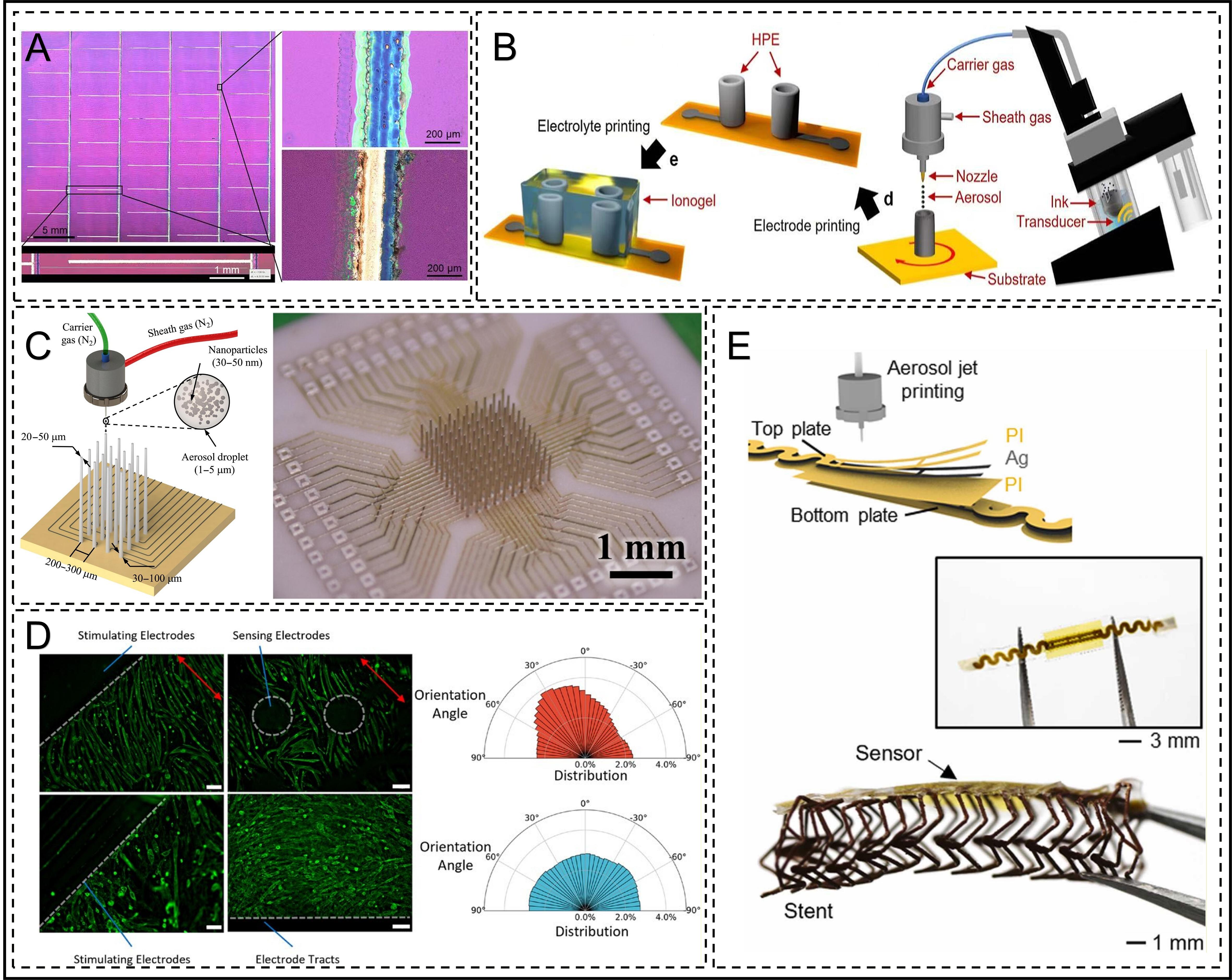
Figure 12. AJP in the applications of energy harvesting and storage, bioelectronics, and biomedical devices. (A) AJP-fabricated photovoltaic interconnection module and enlarged image of the silver grid pattern[47]. Reprinted with permission[47]. Copyright 2024, Energy Technology; (B) AJP fabrication process for three-dimensional graphene supercapacitors[48]. Reprinted with permission[48]. Copyright 2025, ACS Applied Energy Materials; (C) AJP-fabricated microneedle array for electrophysiological recording[49]. Reprinted with permission[49]. Copyright 2022, Science Advances; (D) Cell alignment induced by AJP-printed electrodes[50]. Reprinted with permission[50]. Copyright 2026, Advanced Healthcare Materials; (E) Implantable strain sensor fabricated by AJP and mounted on a wireless stent for real-time monitoring of restenosis[184]. Reprinted with permission[184]. Copyright 2022, Nano Today. AJP: Aerosol jet printing; HPE: hollow pillar electrodes; PI: polyimide.
Thermoelectric energy harvesting represents another area in which AJP offers distinct advantages. Thermoelectric harvesters convert temperature gradients directly into electrical energy through the Seebeck effect. When two dissimilar conductors or semiconductors are electrically connected and their junctions are kept at different temperatures, charge carriers migrate from the hot region to the cold region, generating a measurable voltage. For thermoelectric harvesters, the primary advantage of AJP lies in its ability to deposit conductive features and contacts on flexible, curved, or otherwise irregular substrates, where traditional planar fabrication methods are impractical[222]. Although AJP can provide fine geometric control, high-resolution patterning is generally a secondary consideration because thermoelectric performance is more strongly governed by material properties and thermoelectric coupling than by lateral feature size[223]. Another strength of AJP in this context is its broad material compatibility, which enables the direct deposition of effective thermoelectric materials, such as chalcogenide compounds, including Bi2Te3[224,225], Sb2Te3[226,227], and their combinations[228,229]. Beyond the use of preformulated inks, combinatorial AJP has emerged as an interesting strategy for synthesizing thermoelectric alloys through precursor co-deposition, which facilitates rapid exploration of composition–property relationships[230]. Such approaches generally require post-deposition sintering to achieve adequate electrical connectivity, which can be incompatible with flexible substrates. However, these constraints can be mitigated by nonthermal or low-temperature sintering strategies that preserve substrate integrity[224,231]. From a system-level perspective, thermoelectric harvesters and other passive harvesters[232] are well suited for powering AJP-printed electronic devices with very low power consumption. They support the development of self-sufficient, battery-free systems that operate by harvesting ambient or waste heat and reduce the need for external power wiring.
In electrochemical batteries, most AJP-based studies have focused on the direct printing of active electrode materials[233-236] or on the deposition of solid-state electrolytes[237,238], rather than the fabrication of fully integrated microscale battery architectures. In practice, AJP is more commonly applied to produce electrodes and components at practical, device-relevant dimensions, where its material versatility and three-dimensional deposition capability can be fully exploited. One widely recognized feature of AJP-printed battery electrodes is their inherent micro- and nanoscale porosity, which increases the electrochemically active surface area and improves interfacial charge-transfer kinetics and ion transport[239,240]. This porous morphology, together with the ability of AJP to deposit materials in a controlled layer-by-layer manner, improves electrode utilization compared with dense films produced by conventional coating methods. Furthermore, three-dimensional AJP has been employed to fabricate structured Ag current collectors with tailored architectures, providing improved current distribution within the electrode[241]. Finally, Morzy et al. used AJP to fabricate samples for advanced operando transmission electron microscopy characterization of battery active materials, thereby expanding the range of battery materials and structures compatible with AJP-based characterization[242].
Supercapacitors constitute a complementary energy storage technology that benefits strongly from the geometric freedom afforded by AJP. Their performance is highly dependent on electrode surface area, porosity, and interfacial quality, all of which can be engineered through additive patterning. In contrast to batteries, most AJP-related studies on electrochemical capacitors focus on microscale supercapacitors, which are well suited for powering the low-power flexible devices discussed in the preceding sections because they provide rapid charge-discharge capability and long cycle life[94,243,244]. Using AJP, flexible and stretchable microsupercapacitors have been demonstrated on polymeric and elastomeric substrates, enabling energy storage components that can mechanically conform to flexible electronic systems[85,245,246]. In this regard, Zhou et al. recently demonstrated the fabrication of stretchable microsupercapacitors by AJP electrode materials onto pre-stretched elastomeric substrates, which were then relaxed to induce controlled crumpling of the printed layers[247]. This approach produced devices with nearly unchanged performance even under biaxial 200% × 200% deformation. Moreover, three-dimensional AJP can be used to fabricate structured or vertically integrated electrodes, further increasing the accessible surface area and volumetric capacitance beyond what can be achieved by traditional planar coating or scraping processes, as shown in Figure 12B[48].
Bioelectronics and biomedical devices
Bioelectronics and biomedical devices are often constrained by anatomical structures, mechanical compliance requirements, and sensitivity to processing conditions, which limits the application scope of traditional planar microfabrication techniques. In this context, AJP offers clear advantages because it can deposit functional materials with micrometer-scale precision on soft, flexible, and irregular substrates. These features enable compact system-level integration in wearable and implantable biomedical devices and make AJP a promising manufacturing technology for biomedical engineering.
In addition to the previously mentioned applications, one of the most established biomedical applications of AJP is the fabrication of electrodes and conductive features for neural and electrophysiological interfaces[248,249]. High-resolution traces printed by AJP have been used to define microelectrodes[250], microcoils[251,252], and fine-pitch routing structures for neural stimulation and recording[253]. In particular, electrophysiological interfaces benefit from the ability of AJP to build vertically structured features. In this regard, Saleh et al. demonstrated an AJP-fabricated microneedle array with high probe density and successfully recorded action potentials from a mouse brain [Figure 12C][49]. The ability to process materials such as AgNP inks and conductive polymers on flexible substrates enables mechanically compliant interfaces that better match the elastic modulus of biological tissues. This mechanical compliance is critical for reducing micromotion-induced damage and improving long-term device stability. Moreover, AJP enables direct patterning on curved or irregular implant surfaces, allowing electrode placement and interconnect routing in anatomically relevant geometries that are difficult to address using traditional lithographic techniques.
Tissue engineering and organ-on-a-chip systems are particularly important applications for AJP because they require precise spatial control of materials to regulate cell behavior and mimic native tissue organization. Beyond electrophysiological recording, AJP-fabricated microelectrode arrays can also serve as physical and electrical guidance cues, promoting selective cell adhesion and alignment for advanced tissue engineering, as shown in Figure 12D[50]. More generally, microscale patterning has become a key design parameter for guiding cell adhesion, alignment, migration, and differentiation. Patterned substrates have been shown to promote anisotropic cell organization, such as directed neuronal alignment and neurite outgrowth[254]. AJP can support this control through the direct deposition of conductive polymers, hydrogels, extracellular matrix components, and protein-based inks with high positional accuracy[255]. In scaffold-related applications, AJP has been used to deposit extracellular-matrix-like materials, such as collagen[256,257], in dense and spatially defined architectures with microstructural fidelity relevant to connective tissue environments. Compared to extrusion-based bioprinting, AJP offers finer feature control and compatibility with relatively low-viscosity biomaterials, making it particularly suited for localized scaffold functionalization rather than bulk tissue fabrication. These capabilities also translate naturally to organ-on-a-chip systems, in which multiple material functions must be integrated within confined microfluidic architectures. Such as Rich et al. reduced the time required to manufacture one interdigital transducer using AJP from ~40 h to ~5 min, significantly shortening the development cycle[51]. This approach enabled rapid prototyping of acoustofluidic systems capable of acoustic streaming and particle manipulation for lab-on-chip applications.
Beyond neural interfaces and tissue engineering, AJP has also been widely explored for wearable and implantable medical devices. Wearable health-monitoring systems require electronic components that maintain electrical performance under repeated bending, twisting, or stretching while remaining lightweight and unobtrusive[30,258]. AJP enables direct deposition of conductive traces and circuit elements on elastomers, polymer films, and textile substrates, facilitating the integration of electronics into garments or skin-mounted platforms[259,260]. In implantable devices, the ability to route electrical connections over three-dimensional housings, sharp edges, or stepped topographies supports miniaturization and heterogeneous integration[261]. Herbert et al. reported a fully implantable, battery-free vascular platform in which AJP-printed strain sensors were integrated onto an inductive stent, as shown in Figure 12E. This platform enabled wireless, real-time monitoring of arterial stiffness and restenosis in both arterial models and ex vivo coronary arteries[184]. Moreover, proteins and other biomolecules have been deposited by AJP without significant loss of activity, enabling the patterned presentation of adhesion ligands, signaling molecules, and biochemical gradients[136]. This capability expands the design space for engineered microenvironments in which biological responses can be modulated through spatially defined chemical cues, supporting applications in in vitro disease modeling, drug screening, and tissue development studies[262].
Overall, the biomedical relevance of AJP lies in its versatility as an enabling fabrication platform rather than in a single application area. Its ability to combine high-resolution patterning, conformal deposition, and multi-material compatibility addresses key challenges in neural interfaces, wearable and implantable electronics, tissue-engineered substrates, and organ-on-a-chip systems. As printable biomaterials and low-temperature processing strategies continue to advance, AJP is expected to play an increasingly important role in niche and high-value biomedical applications, where geometric complexity and multi-material integration are more important than the advantages of conventional mass-production technologies.
Across the four application domains discussed in this section, AJP provides a common advantage through its conformal deposition capability, material versatility, and mask-less direct-write process. These features allow functional components to be integrated onto substrates and geometries that are difficult to process using conventional microfabrication. In flexible and printed electronics, this advantage enables high-resolution patterning on mechanically compliant substrates. In sensors and actuators, it supports compact multi-material architectures with tailored transduction properties. In energy devices, it enables structured electrodes and conformal harvesters on irregular surfaces. In biomedical systems, it supports mechanically compliant interfaces that match the complexity of biological environments. Across these fields, the same characteristics also make AJP suitable for rapid prototyping and small-batch production. However, challenges related to print consistency, long-term reliability, and scalability still need to be addressed. These issues are discussed in the following section in the broader context of the development trajectory of AJP.
CONCLUSIONS AND OUTLOOK
Conclusions
This review systematically summarizes the recent progress of AJP in the fabrication of micro-nano scale functional structures and the manufacturing of complex surfaces, with particular emphasis on the demands of flexible electronics. Starting from the fundamental working principles of AJP, this review discusses the key processes of aerosol generation, aerodynamic focusing, material deposition, and post-processing. Particular attention is paid to the physical mechanisms that govern printing resolution, morphological uniformity, and functional performance. These mechanisms directly affect jet stability, droplet evaporation, and final deposition morphology. Representative process optimization strategies reported in recent years are also reviewed, including jet stabilization, multi-physics assisted control, deposition morphology regulation, and conformal printing on complex geometries and flexible substrates.
The reviewed studies indicate that AJP achieves a unique balance among printing resolution, material compatibility, and three-dimensional conformal manufacturability. By rationally tuning the coupling between the carrier gas and sheath gas and introducing auxiliary physical fields, such as thermal, acoustic, or solvent-vapor fields, the stability and focusing quality of the aerosol jet can be effectively improved. These strategies suppress overspray and edge blurring, thereby improving the geometric accuracy and edge sharpness of printed lines. At the deposition and post-processing stages, this review summarizes various low-temperature and substrate-compatible processing strategies for flexible substrates, including thermal sintering, photonic sintering, plasma sintering, and related methods. These techniques enable precise control of structural densification, microstructural evolution, and functional properties. As a result, they improve the electrical conductivity, flexibility, mechanical robustness, and long-term stability of printed features. In other words, process parameters affect the microstructure of the deposited layer, which in turn determines the electrical and mechanical properties of the device.
From a materials perspective, AJP has been extended to a broad range of ink systems, including metallic nanoparticles, MOD inks, carbon-based materials, selected semiconductor and dielectric formulations, and bio-inks. The rheological properties of the ink strongly influence atomization efficiency and jet focusing quality, thereby determining whether high-precision printing can be achieved across different material systems. In particular, this review highlights stretchable and low-temperature-curable conductive inks developed for flexible electronics, which show strong versatility and scalability. In terms of applications, AJP has shown strong potential in flexible electronics, wearable devices, patch antennas, physical and chemical sensors, micro-energy systems, and bioelectronics. These applications are closely related to flexible and wearable scenarios and demonstrate the ability of AJP to achieve functional integration on complex three-dimensional substrates. Overall, this review focuses on the intersection between flexible electronics and additive manufacturing.
At present, AJP is evolving from a laboratory-scale high-resolution patterning technique into a more general additive manufacturing platform for flexible substrates and complex three-dimensional structures. Accordingly, the research focus is shifting from isolated process-parameter optimization to integrated design strategies involving multiscale, multi-physics, and multisystem coordination. However, AJP still faces several key challenges for practical engineering applications. These challenges include the long-term reliability of flexible components, such as performance degradation under thermal cycling, mechanical bending, humid environments, and interfacial delamination. They also include limitations in scalable manufacturing, such as low single-nozzle throughput, poor consistency among multiple nozzles, and insufficient long-term printing stability. In addition, material and process constraints, including ink storage stability, nozzle clogging, and defects during curved-surface deposition, remain unresolved. Systematic studies on these engineering challenges are still limited. Therefore, future research should place greater emphasis on reliability, scalability, material stability, and process robustness to accelerate the transition of AJP from laboratory demonstrations to practical manufacturing.
Outlook
Despite the substantial progress achieved to date, AJP still faces several challenges printing consistency, reliability, and large-scale manufacturing. Future research directions can be broadly summarized as follows.
(1) Systematic modeling and unified theory of multi-physics coupling
Current theoretical studies on AJP are mostly limited to individual process stages, and a unified multi-physics framework covering the entire workflow, from aerosol formation and transport to jet focusing, deposition, and solidification, is still lacking. Future efforts should integrate CFD, multiphase flow, heat and mass transfer, and phase-transformation kinetics to establish high-fidelity predictive models. These models should correlate process parameters with printing morphology and functional performance, thereby enabling rational process design and improved reproducibility.
(2) Intelligent conformal printing systems for complex surfaces
As AJP applications expand from planar substrates to complex freeform geometries, printing quality increasingly depends on the dynamic geometric relationship between the nozzle and the substrate. The development of next-generation AJP systems is expected to focus on intelligent integration of perception, planning, and printing. By incorporating three-dimensional vision or laser-based surface sensing, adaptive path-planning algorithms, and multi-axis motion platforms, these systems could enable real-time adjustment of nozzle orientation, stand-off distance, and deposition angle. Specifically, reinforcement-learning-based online path correction should be explored to address the dynamic deformation of flexible substrates, which cannot be effectively handled by traditional offline programming.
(3) Synergistic development of high-performance inks
Although AJP exhibits strong material compatibility, long-term ink stability, deposition uniformity, and interfacial reliability of printed structures remain critical bottlenecks for practical applications. Future work should emphasize the coordinated optimization of ink formulations, solvent systems, additives, and substrate surface engineering. A closed-loop database linking ink formulation, process parameters, and device performance should also be established. In parallel, integrated screening approaches that combine high-throughput experimentation and machine learning should be developed to accelerate the discovery and optimization of new functional inks.
(4) Application-oriented reliability assessment and scalable manufacturing
Many existing studies primarily focus on proof-of-concept demonstrations, whereas systematic investigations of device reliability under thermal cycling, mechanical deformation, and long-term operation remain limited. Future work should clarify the failure mechanisms of AJP-printed structures and explore scalable manufacturing pathways, such as integration with roll-to-roll processing, parallel printing, and multi-nozzle architectures. These efforts are essential for facilitating the transition of AJP from prototyping to practical engineering deployment.
(5) AI- and data-driven process intelligence
Traditional process optimization relies on sequential single-parameter scanning, which is inefficient and cannot fully capture multiparameter coupling effects. In future work, machine learning methods, such as Gaussian process regression and neural networks, should be used to establish nonlinear mapping models between input parameters, including gas flow rate, FR, temperature, and ink viscosity, and output metrics, including linewidth, conductivity, and edge roughness. These models could enable rapid exploration of the parameter space and inverse process design. Furthermore, in situ monitoring techniques, such as light scattering and machine vision, can be integrated with closed-loop feedback control to establish an intelligent print-measure-learn-adjust loop. This strategy could fundamentally transform empirical trial-and-error-based parameter tuning into data-driven process optimization.
In summary, AJP is at a critical stage of transition from a process-driven paradigm to a system- and data-driven paradigm. With the continued integration of multi-physics modeling, intelligent hardware, advanced materials, and AI methodologies, AJP is expected to play an increasingly important role in flexible and wearable systems, three-dimensional conformal electronics, biomedical devices, and heterogeneous integration technologies.
DECLARATIONS
Authors’ contributions
Conceptualization: Chen, X. (Xiaoming Chen); Chen, X. (Xiaoliang Chen); Magagnin, L.
Writing: Zhao, H.; Viviani, P.; Zhao, Q.; Han, T.; Lissandrello, F.
Review and editing: Zhao, H.; Zhang, J.; Chen, X. (Xiaoming Chen)
Figure preparation: Zhao, H.; Viviani, P.; Han, T.; Lissandrello, F.
All authors contributed to the editing and approved the final version of the manuscript.
All authors have read and agreed to the published version.
Availability of data and materials
Not applicable.
AI and AI-assisted tools statement
During the preparation of this work, the author(s) used Chat GPT (Open AI, version GPT-5 mini, released 2023-10) and Dou bao (Byte Dance, version 3.5, released 2025-10) due to the need for rapid generation of schematic symbols and basic graphic elements required for Figure 2, which were subsequently manually refined and redrawn by the authors. The author(s) reviewed and edited all AI-generated content and accept full responsibility for the published material.
Financial support and sponsorship
This work was supported by Grant name National Natural Science Foundation of China (No. 525B2084; No. 52575638).
Conflicts of interest
All authors declared that there are no conflicts of interest.
Ethical approval and consent to participate
Not applicable.
Consent for publication
Not applicable.
Copyright
© The Author(s) 2026.
REFERENCES
1. Jian, W.; Chen, Y.; Feng, X. 3D conformal curvy electronics: design, fabrication, and application. ACS. Nano. 2025, 19, 15177-88.
2. Liu, G.; Li, X.; Chen, X.; et al. Printing high-resolution conformal electronics on meter-scale surfaces using template-confined microfluidics. Mater. Today. 2025, 83, 166-80.
3. Pan, J.; Zhao, W.; Zhou, Y.; et al. Conformal electronics: materials, fabrication, and emerging applications. FlexMat 2025, 2, 341-64.
4. Rurup, J. D.; Secor, E. B. In-situ qualification and physics-based process design for aerosol jet printing via spatially correlated light scattering measurements. Addit. Manuf. 2024, 82, 104037.
5. Zhang, S.; Zhao, Y.; Wang, Y.; Chen, R.; Liu, Y.; Wei, D. Photolithographic organic electronics: from material design to applications. Chem. Soc. Rev. 2025, 54, 6610-33.
6. Bathaei, M. J.; Singh, R.; Mirzajani, H.; et al. Photolithography-based microfabrication of biodegradable flexible and stretchable sensors. Adv. Mater. 2023, 35, e2207081.
7. Lei, H.; Patel, T.; Lopez, J.; Devin Mackenzie, J. Screen-printed flexible antennas for 24-GHz ISM band and mmWave applications. IEEE. Flex. Electron. 2025, 4, 138-45.
8. Chen, Z.; Zhang, C.; Zheng, Z. Advancements in transfer printing techniques for flexible electronics: adjusting interfaces and promoting versatility. Int. J. Extrem. Manuf. 2024, 6, 052005.
9. Zhao, Q.; Li, K.; Sun, F.; et al. A versatile transfer printing technique through soap bubble. npj. Flex. Electron. 2025, 9, 460.
10. Li, J.; Feng, Y.; Cao, Z.; et al. Inkjet‐printed high‐throughput screening of ultrafast polymer‐stabilized blue‐phase liquid crystals for electrically adaptive microlens. Adv. Funct. Mater. 2026, e75246.
11. Cong, C.; Li, X.; Xiao, W.; et al. Electrohydrodynamic printing for demanding devices: a review of processing and applications. Nanotechnol. Rev. 2022, 11, 3305-34.
12. Yin, Z.; Wang, D.; Guo, Y.; et al. Electrohydrodynamic printing for high resolution patterning of flexible electronics toward industrial applications. InfoMat 2024, 6, e12505.
13. Iranshahi, K.; Defraeye, T.; Rossi, R. M.; Müller, U. C. Electrohydrodynamics and its applications: recent advances and future perspectives. Int. J. Heat. Mass. Transf. 2024, 232, 125895.
14. Bi, S.; Wang, R.; Han, X.; et al. Recent progress in electrohydrodynamic jet printing for printed electronics: from 0D to 3D materials. Coatings 2023, 13, 1150.
15. Cho, Y.; Beak, J. W.; Sagong, M.; Ahn, S.; Nam, J. S.; Kim, I. D. Electrospinning and nanofiber technology: fundamentals, innovations, and applications. Adv. Mater. 2025, 37, e2500162.
16. Keirouz, A.; Wang, Z.; Reddy, V. S.; et al. The history of electrospinning: past, present, and future developments. Adv. Mater. Technol. 2023, 8, 2201723.
17. Nadaf, A.; Gupta, A.; Hasan, N.; et al. Recent update on electrospinning and electrospun nanofibers: current trends and their applications. RSC. Adv. 2022, 12, 23808-28.
18. Li, X.; Shan, W.; Yang, Y.; et al. Limpet tooth‐inspired painless microneedles fabricated by magnetic field‐assisted 3D printing. Adv. Funct. Mater. 2021, 31, 2003725.
19. Ma, Z.; Wu, Y.; Lu, S.; et al. Magnetically assisted 3D printing of ultra‐antiwear flexible sensor. Adv. Funct. Mater. 2024, 34, 2406108.
20. Tian, Y.; Zhou, J.; Zhu, H.; et al. Electrohydrodynamic printing technology: mechanisms, control, and applications. Microsyst. Nanoeng. 2026, 12, 83.
21. Panáček, D.; Urban, M.; Silvestri, A.; et al. Nanomaterial-based inkjet printing for electrochemical sensing. Small 2026, 22, e13028.
22. Islam, M. S.; Zorman, C. A.; Cao, C. Parametric optimization of PEDOT:PSS aerosol jet printing for enhanced line morphology in flexible electronics. Adv. Electron. Mater. 2026, 12, e00535.
23. Fapanni, T.; Sardini, E.; Serpelloni, M. A preliminary study on flexible temperature sensors for eskin medical devices. In Proceedings of the 25th IMEKO TC4 International Symposium, Brescia, Italy, Sep 12-14, 2022. 2022; pp. 277-81. https://iris.unibs.it/retrieve/handle/11379/575266/189944/IMEKO-TC4-2022-51.pdf. (accessed 2026-06-05).
24. Yi, H.; Liu, Y.; Cao, H.; et al. Material and process integrated innovations in aerosol jet printing: a review. Mater. Today. 2025, 91, 431-58.
25. Zhang, J.; Zhu, H.; Liu, D.; Li, Y.; Huang, C. Piezoelectric inkjet printing: the principles, fluid dynamics challenges, and applications. Mater. Today. Commun. 2024, 41, 110866.
26. Li, Y.; Zhang, G.; Zhang, J.; et al. Advanced multi-nozzle electrohydrodynamic printing: mechanism, processing, and diverse applications at micro/nano-scale. Int. J. Extrem. Manuf. 2025, 7, 012008.
27. Taccola, S.; da Veiga, T.; Chandler, J. H.; Cespedes, O.; Valdastri, P.; Harris, R. A. Micro-scale aerosol jet printing of superparamagnetic Fe3O4 nanoparticle patterns. Sci. Rep. 2022, 12, 17931.
28. Tafoya, R. R.; Gallegos, M. A.; Downing, J. R.; et al. Morphology and electrical properties of high-speed flexography-printed graphene. Mikrochim. Acta. 2022, 189, 123.
29. Tonello, S.; Fapanni, T.; Bonaldo, S.; et al. Amperometric measurements by a novel aerosol jet printed flexible sensor for wearable applications. IEEE. Trans. Instrum. Meas. 2023, 72, 1-12.
30. Perilli, S.; Di Pietro, M.; Mantini, E.; et al. Development of a wearable electromyographic sensor with aerosol jet printing technology. Bioengineering 2024, 11, 1283.
31. Degryse, O.; Bloemen, V.; Ferraris, E. Collagen composite inks for Aerosol Jet® printing in bone tissue engineering applications. Procedia. CIRP. 2022, 110, 180-5.
32. Derman, I. D.; Kim, M. H.; Sarikaya, M. D.; et al. Unconventional bioprinting modalities for advanced tissue biofabrication. Biomaterials 2026, 326, 123704.
33. Gupta, E.; Bonner, C.; Lazarus, N.; Mirotznik, M. S.; Nicholson, K. J. Multiaxis manufacture of conformal metasurface antennas. Antennas. Wirel. Propag. Lett. 2023, 22, 2629-33.
34. Gohel, A.; Gratuze, M.; Ketabi, M.; Izquierdo, R. Direct-write printing for flexible and 3D electronics: aerosol jet vs. micro dispensing. Micromachines 2025, 16, 931.
35. Jeong, H.; Lee, J. H.; Kim, S.; et al. Optimization of process parameters in micro-scale pneumatic aerosol jet printing for high-yield precise electrodes. Sci. Rep. 2023, 13, 21297.
36. Zhang, H.; Choi, J. P.; Liu, X.; et al. LLM-inspired vision transformer framework for intelligent quality recognition in aerosol jet printing. Engineering 2026, In Press.
37. Wang, B.; Zhang, H.; Choi, J. P.; Moon, S. K.; Lee, B.; Koo, J. A post-treatment method to enhance the property of aerosol jet printed electric circuit on 3D printed substrate. Materials 2020, 13, 5602.
38. Rurup, J. D.; Secor, E. B. Understanding oblique deposition in aerosol jet printing for conformal electronics fabrication. J. Manuf. Process. 2024, 120, 1231-40.
39. Ma, T.; Li, Y.; Cheng, H.; et al. Enhanced aerosol-jet printing using annular acoustic field for high resolution and minimal overspray. Nat. Commun. 2024, 15, 6317.
40. Ma, T.; Li, Y.; Li, A.; et al. Nozzle heating with internal channel enhanced aerosol-jet printing with ultrahigh aspect ratio and ultrafine resolution for conformal electronics. Addit. Manuf. 2025, 111, 104965.
41. Wei, W.; Zhang, L.; Liao, Z.; Cai, Y. Aerosol jet printing of advanced capacitive strain gauge for vibration monitoring of the human body. Int. J. Adv. Manuf. Technol. 2025, 138, 31-43.
42. Li, L.; Zhang, K.; Cheng, H.; et al. Experimental and simulation investigations on the morphology of aerosol jet printed polymer traces under in-situ UV and thermal curing conditions. Addit. Manuf. 2023, 69, 103515.
43. Jignasu, A.; Rurup, J. D.; Secor, E. B.; Krishnamurthy, A. NURBS-based path planning for aerosol jet printing of conformal electronics. J. Manuf. Process. 2024, 118, 187-94.
44. Hobbie, H. A.; Doherty, J. L.; Smith, B. N.; Maccarini, P.; Franklin, A. D. Conformal printed electronics on flexible substrates and inflatable catheters using lathe-based aerosol jet printing. Npj. Flex. Electron. 2024, 8, 54.
45. Ghosh, S. K.; Kepros, E.; Chahal, P. Aerosol-jet printed high-Q quasi-optical FSSs on flex substrates using a novel parylene lift-off process. IEEE. Trans. Compon. Packag. Manuf. Technol. 2025, 15, 244-52.
46. Alexandre, E. B.; Corzo, D.; Lengger, S.; Carrara, S.; Kosel, J. Imperceptible and disposable humidity and temperature sensors with low environmental footprint enabled by aerosol jet printing and cellulose-based substrates. Small. Methods. 2026, 10, e2500506.
47. Vlnieska, V.; Siegrist, S.; Ceres, P. O. Q.; Heier, J.; Fu, F.; Romanyuk, Y. E. Monolithic interconnection of thin‐film perovskite photovoltaic modules using aerosol jet printing. Energy. Technol. 2025, 13, 2401793.
48. Zhong, X.; Du, J.; Gu, Y.; Lu, Z.; Hyun, W. J. 3D aerosol-jet-printable graphene microsupercapacitor arrays with hollow pillar electrodes for high voltage and integration density. ACS. Appl. Energy. Mater. 2025, 8, 18336-45.
49. Saleh, M. S.; Ritchie, S. M.; Nicholas, M. A.; et al. CMU array: a 3D nanoprinted, fully customizable high-density microelectrode array platform. Sci. Adv. 2022, 8, eabj4853.
50. Cheah, E.; Gao, X.; Jaw, W. Q.; et al. Customizable fabrication of 2D and conformal multielectrode arrays for 3D printed organotypic bioelectronic interfaces. Adv. Healthc. Mater. 2026, 15, e02757.
51. Rich, J.; Cole, B.; Li, T.; et al. Aerosol jet printing of surface acoustic wave microfluidic devices. Microsyst. Nanoeng. 2024, 10, 2.
52. Zhang, H.; Xu, H.; Cui, L.; et al. An extensive study of the influence of key flow variables on printed line quality outcomes during aerosol jet printing using coupled three-dimensional numerical models. Materials 2024, 17, 3179.
53. Xin, M.; Wu, Y.; Yang, Y. Combinatorial aerosol printing of mechanochromic materials. Matter 2026, 9, 102696.
54. Schwartz, A. J.; Rurup, J. D.; Secor, E. B. Closing the loop on pneumatic atomization for shift-length aerosol jet printing with real-time light scattering measurements. J. Manuf. Process. 2025, 152, 631-7.
55. Feng, J.; Klett, J. D.; Renn, M. J. Mist generation behavior in ultrasonic atomizer for Aerosol Jet® printing. Aerosol. Sci. Eng. 2024, 8, 77-86.
56. Ballesteros Martínez, M. Á.; Becerra, D.; Gaukel, V. Modelling the flow conditions and primary atomization of an air-core-liquid-ring (ACLR) atomizer using a coupled eulerian–lagrangian approach. Flow. Turbulence. Combust. 2024, 113, 437-58.
57. Schäfer, W.; Rosenkranz, S.; Brinckmann, F.; Tropea, C. Analysis of pneumatic atomizer spray profiles. Particuology 2016, 29, 80-5.
58. Khmelev, V. N.; Shalunov, A. V.; Golykh, R. N.; Nesterov, V. A.; Dorovskikh, R. S.; Shalunova, A. V. Providing the efficiency and dispersion characteristics of aerosols in ultrasonic atomization. J. Eng. Phys. Thermophy. 2017, 90, 831-44.
59. Ebrahimiazar, M.; Ashgriz, N. Aerosol generation by ultrasonic atomization of nanoliter liquid volumes. Phys. Fluids. 2025, 37, 047153.
60. Qin, R.; Duan, C. The principle and applications of Bernoulli equation. J. Phys. Conf. Ser. 2017, 916, 012038.
61. Gamba, L.; Johnson, Z. T.; Atterberg, J.; et al. Systematic design of a graphene ink formulation for aerosol jet printing. ACS. Appl. Mater. Interfaces. 2023, 15, 3325-35.
62. Jiang, X.; Yan, Z.; Niu, Y.; et al. Enhanced morphology and conductivity in aerosol jet printing via optimization of print speed range under various deposition rate. Mater. Design. 2025, 259, 114745.
63. Li, G.; Wang, S.; Zhang, Z.; et al. Precision control of aerosol jet printing for conformal electronics fabrication with ultra‐fine and wide‐range resolution. Adv. Mater. Technol. 2025, 10, 2402114.
64. Efimov, A.; Arsenov, P.; Kornyushin, D.; Lizunova, A.; Volkov, I.; Ivanov, V. Aerosol jet printing of silver lines with a high aspect ratio on a heated silicon substrate. Materials 2020, 13, 730.
65. Vyas, A.; Ng, S.; Anum, I. A highly sensitive, biodegradable capacitive humidity sensor with aerosol jet printed electrodes on a self-standing CMC film. J. Mater. Chem. C. 2025, 13, 21154-69.
66. Huang, B.; Wu, S.; Liu, J.; Liu, J.; Peng, B.; Zhou, Z. Aerosol jet printing of polyelectrolyte-modified MXene ink for a multifunctional humidity and temperature flexible sensor. Chem. Eng. J. 2025, 519, 165403.
67. Bappy, M. O.; Tanvir, A. N. M.; Song, K.; Jiang, Q.; Du, Y.; Zhang, Y. Aerosol jet printing and photonic flash sintering of a flexible multimodal sensor for concurrent temperature and strain sensing. ACS. Appl. Electron. Mater. 2025, 7, 6265-72.
68. Zhou, X.; Zhang, L.; Zhang, S.; et al. Self-assembly of 3D-printed multiscale micropillar-based organic electrochemical transistors for ultrasensitive dopamine sensing. ACS. Nano. 2025, 19, 39615-27.
69. Gamba, L.; Diaz-Arauzo, S.; Hersam, M. C.; Secor, E. B. Aerosol jet printing of phase-inversion graphene inks for high-aspect-ratio printed electronics and sensors. ACS. Appl. Nano. Mater. 2023, 6, 21133-40.
70. Wang, Z.; Xu, J.; Niu, Y.; Tan, Y.; Yang, B.; Yi, C. Fabrication of highly sensitive conformal temperature sensors on stainless steel via aerosol jet printing. J. Manuf. Mater. Process. 2026, 10, 41.
71. Chen, G.; Gu, Y.; Tsang, H.; Hines, D. R.; Das, S. The effect of droplet sizes on overspray in aerosol‐jet printing. Adv. Eng. Mater. 2018, 20, 1701084.
72. Tafoya, R. R.; Secor, E. B. Understanding and mitigating process drift in aerosol jet printing. Flex. Print. Electron. 2020, 5, 015009.
73. Mosa, M. A.; Jo, J. Y.; Kwon, K. Enhanced aerosol jet printing: leveraging jet visualization for increased stand-off distances. J. Manuf. Process. 2024, 131, 694-706.
74. Wang, J.; Yu, G.; Ai, J.; et al. Fabrication and optimization of aerosol-jet-printed temperature sensors on carbon fiber-reinforced composites. ACS. Appl. Electron. Mater. 2026, 8, 2493-503.
75. Chung, S.; Kim, Y.; Lee, C. Computational study of the particle distribution in aerosol flow in the aerosol jet printing process. Int. J. Precis. Eng. Manuf. 2025, 26, 989-98.
76. Feng, J. Q.; Ramm, A.; Renn, M. J. A quantitative analysis of overspray in Aerosol Jet® printing. Flex. Print. Electron. 2021, 6, 045006.
77. Mahajan, B. K.; Ludwig, B.; Shou, W.; et al. Aerosol printing and photonic sintering of bioresorbable zinc nanoparticle ink for transient electronics manufacturing. Sci. China. Inf. Sci. 2018, 61, 9366.
78. Gamba, L.; Razzaq, M. E. A.; Diaz-Arauzo, S.; Hersam, M. C.; Bai, X.; Secor, E. B. Tailoring electrical properties in carbon nanomaterial patterns with multimaterial aerosol jet printing. ACS. Appl. Mater. Interfaces. 2023, 15, 57525-32.
79. Ramesh, S.; Mahajan, C.; Gerdes, S.; et al. Numerical and experimental investigation of aerosol jet printing. Addit. Manuf. 2022, 59, 103090.
80. Jin, Y.; Yi, H.; Cao, H.; Dong, X. Full-process aerosol jet printing modelling: achieving high-fidelity simulation via coupling jetting and deposition. Virtual. Phys. Prototyp. 2025, 20, e2516665.
81. Guyll, B. I.; Sanford, B. L.; Pint, C. L.; Secor, E. B. Controlling droplet evaporation in aerosol jet printing to understand and mitigate overspray. Small. Sci. 2025, 5, 2500069.
82. Park, J.; Jeong, J.; Kim, C.; Hwang, J. Deposition of charged aerosol particles on a substrate by collimating through an electric field assisted coaxial flow nozzle. Aerosol. Sci. Technol. 2013, 47, 512-9.
83. Seifert, T.; Sowade, E.; Roscher, F.; Wiemer, M.; Gessner, T.; Baumann, R. R. Additive manufacturing technologies compared: morphology of deposits of silver ink using inkjet and aerosol jet printing. Ind. Eng. Chem. Res. 2015, 54, 769-79.
84. Winnicki, M.; Łapa, W.; Świadkowski, B. A novel approach to improve reliability of aerosol jet printing process. Maint. Reliab. 2024, 26, 180012.
85. Kouchi, F. R.; Varghese, T. V.; Burgoyne, H.; et al. StableTi3C2Tx MXene ink formulation and high-resolution aerosol jet printing for high-performance MXene supercapacitors. Small. Methods. 2025, 9, e2500499.
86. Sui, Y.; Tsui, L.; Thibodeaux, A. J.; Lavin, J. M. An aerosol jet printed resistance temperature detector‐micro hotplate with temperature coefficient of resistance stabilized by electrical sintering. Adv. Mater. Technol. 2023, 8, 2202053.
87. Beedasy, V.; Smith, P. J. Printed electronics as prepared by inkjet printing. Materials 2020, 13, 704.
88. Sung, K.; Park, J.; Kang, H. Multi-layer inkjet printing of Ag nanoparticle inks and its sintering with a near-infrared system. Int. J. Precis. Eng. Manuf. 2018, 19, 303-7.
89. Keller, D. J.; Jochem, K. S.; Suszynski, W. J.; Francis, L. F. Near-IR sintering of conductive silver nanoparticle ink with in situ resistance measurement. J. Coat. Technol. Res. 2019, 16, 1699-705.
90. Chen, I.; Liu, Y.; Yu, X.; et al. Aerosol printing and flash sintering of conformal conductors on 3D nonplanar surfaces. Manuf. Lett. 2022, 31, 119-23.
91. Du, Y.; Yang, J.; Song, K.; et al. Autonomous aerosol and plasma co-jet printing of metallic devices at ambient temperature. Small 2025, 21, e2409751.
92. Gibertini, E.; Gervasini, L. F.; Albertazzi, J.; et al. Reactive aerosol jet printing of Ag nanoparticles: a new tool for SERS substrate preparation. Coatings 2025, 15, 900.
93. Rosker, E. S.; Barako, M. T.; Nguyen, E.; et al. Approaching the practical conductivity limits of aerosol jet printed silver. ACS. Appl. Mater. Interfaces. 2020, 12, 29684-91.
94. Luo, Y.; Zhu, Q.; Cao, L.; Fan, L.; Gu, F.; Xiong, S. Aerosol jet printing of hybrid Ti3C2Tx MXene/PEDOT:PSS nanospheres for flexible planar/fiber architectured micro‐supercapacitors. Adv. Eng. Mater. 2025, 27, 2500044.
95. Xu, B.; Yang, M.; Cheng, W.; et al. Precision aerosol-jet micropatterning of liquid metal for high-performance flexible strain sensors. Nat. Commun. 2025, 16, 7920.
96. Arabpoor, R.; Haghighi, A. Experimental insights into aerosol jet printing on 3D curved surfaces: line morphology and resistivity. Manuf. Lett. 2025, 46, 133-7.
97. Fisher, C.; Skolrood, L. N.; Li, K.; Joshi, P. C.; Aytug, T. Aerosol‐jet printed sensors for environmental, safety, and health monitoring: a review. Adv. Mater. Technol. 2023, 8, 2300030.
98. Wilkinson, N. J.; Smith, M. A. A.; Kay, R. W.; Harris, R. A. A review of aerosol jet printing - a non-traditional hybrid process for micro-manufacturing. Int. J. Adv. Manuf. Technol. 2019, 105, 4599-619.
99. Huang, Q.; Zhu, Y. Printing conductive nanomaterials for flexible and stretchable electronics: a review of materials, processes, and applications. Adv. Mater. Technol. 2019, 4, 1800546.
100. Niam, A. G.; Sucahyo, L. Ultrasonic atomizer application for low cost aeroponic chambers (LCAC): a review. IOP. Conf. Ser. Earth. Environ. Sci. 2020, 542, 012034.
101. Binder, S.; Glatthaar, M.; Rädlein, E. Analytical investigation of aerosol jet printing. Aerosol. Sci. Technol. 2014, 48, 924-9.
102. Secor, E. B.; Yeboah, D.; Gamba, L. Additive electronics manufacturing via droplet jetting technologies: materials, methods, applications, and opportunities. Nanoscale 2025, 17, 18997-9020.
103. He, B.; Yang, S.; Qin, Z.; Wen, B.; Zhang, C. The roles of wettability and surface tension in droplet formation during inkjet printing. Sci. Rep. 2017, 7, 11841.
104. Sukeshini A, M.; Meisenkothen, F.; Gardner, P.; Reitz, T. L. Aerosol Jet® Printing of functionally graded SOFC anode interlayer and microstructural investigation by low voltage scanning electron microscopy. J. Power. Sources. 2013, 224, 295-303.
105. Yang, C.; Zhou, E.; Miyanishi, S.; Hashimoto, K.; Tajima, K. Preparation of active layers in polymer solar cells by aerosol jet printing. ACS. Appl. Mater. Interfaces. 2011, 3, 4053-8.
106. May, K. The collison nebulizer: description, performance and application. J. Aerosol. Sci. 1973, 4, 235-43.
107. Yu, J.; Khuje, S.; Sheng, A.; Kilczewski, S.; Parker, T.; Ren, S. High‐temperature copper–graphene conductors via aerosol jetting. Adv. Eng. Mater. 2022, 24, 2200284.
108. Kwon, Y.; Kim, J.; Kim, H.; et al. Printed nanomaterials for all-in-one integrated flexible wearables and bioelectronics. ACS. Appl. Mater. Interfaces. 2024, 16, 68016-26.
109. Doddapaneni, V. V. K.; Lee, K.; Aysal, H. E.; et al. A review on progress, challenges, and prospects of material jetting of copper and tungsten. Nanomaterials 2023, 13, 2303.
110. Jahan, S.; Hu, C.; Yuan, B.; Ritchie, S. M.; Panat, R. Aerosol jet 3D printing of gold micropillars and their behavior under compressive loads. Addit. Manuf. 2024, 92, 104385.
111. Valayil Varghese, T.; Eixenberger, J.; Rajabi-Kouchi, F.; et al. Multijet gold nanoparticle inks for additive manufacturing of printed and wearable electronics. ACS. Mater. Au. 2024, 4, 65-73.
112. Rahman, M. T.; Panat, R. Aerosol jet 3D printing and high temperature characterization of nickel nanoparticle films. Manuf. Lett. 2021, 29, 5-10.
113. McKibben, N.; Curtis, M.; Maryon, O.; et al. Formulation and aerosol jet printing of nickel nanoparticle ink for high-temperature microelectronic applications and patterned graphene growth. ACS. Appl. Electron. Mater. 2024, 6, 748-60.
114. Niu, Y.; Wang, Z.; Li, Y.; et al. Ultrathin MXene/Ag-Ag nanocomposite films for 3D-conformal electromagnetic shielding via aerosol jet printing. Chem. Eng. J. 2025, 506, 160122.
115. Mishra, B.; Chen, Y. M. All-aerosol-jet-printed carbon nanotube transistor with cross-linked polymer dielectrics. Nanomaterials 2022, 12, 4487.
116. Filippi, F.; Fiori, G.; Genovesi, A.; et al. Preliminary characterization of a novel aerosol jet-printed strain sensor for feasibility assessment in a variable stiffness arterial simulator application. Sensors 2024, 24, 7725.
117. Parate, K.; Pola, C. C.; Rangnekar, S. V.; et al. Aerosol-jet-printed graphene electrochemical histamine sensors for food safety monitoring. 2D. Mater. 2020, 7, 034002.
118. Al Shboul, A.; Ketabi, M.; Skaf, D.; et al. Graphene inks printed by aerosol jet for sensing applications: the role of dispersant on the inks’ formulation and performance. Sensors 2023, 23, 7151.
119. Ali, M. A.; Hu, C.; Jahan, S.; et al. Sensing of COVID-19 antibodies in seconds via aerosol jet nanoprinted reduced-graphene-oxide-coated 3D electrodes. Adv. Mater. 2021, 33, e2006647.
120. Tarabella, G.; Vurro, D.; Lai, S.; D’Angelo, P.; Ascari, L.; Iannotta, S. Aerosol jet printing of PEDOT:PSS for large area flexible electronics. Flex. Print. Electron. 2020, 5, 014005.
121. Seiti, M.; Ginestra, P. S.; Ferraro, R. M.; et al. Aerosol Jet® Printing of poly(3,4-ethylenedioxythiophene): poly(styrenesulfonate) onto micropatterned substrates for neural cells in vitro stimulation. Int. J. Bioprint. 2022, 8, 504.
122. Fisher, C.; Warmack, B. J.; Yu, Y.; et al. All-aerosol-jet-printed highly sensitive and selective polyaniline-based ammonia sensors: a route toward low-cost, low-power gas detection. J. Mater. Sci. 2021, 56, 12596-606.
123. Douglas, S. P.; Mrig, S.; Knapp, C. E. MODs vs. NPs: vying for the future of printed electronics. Chemistry 2021, 27, 8062-81.
124. Sheng, A.; Islam, A.; Khuje, S.; et al. Molecular copper decomposition ink for printable electronics. Chem. Commun. 2022, 58, 9484-7.
125. Kell, A. J.; Paquet, C.; Mozenson, O.; et al. Versatile molecular silver ink platform for printed flexible electronics. ACS. Appl. Mater. Interfaces. 2017, 9, 17226-37.
126. Farr, N. T. H.; Davies, M.; Nohl, J.; et al. Revealing the morphology of ink and aerosol jet printed palladium-silver alloys fabricated from metal organic decomposition inks. Adv. Sci. 2024, 11, e2306561.
127. Gupta, A. A.; Arunachalam, S.; Cloutier, S. G.; Izquierdo, R. Fully aerosol-jet printed, high-performance nanoporous ZnO ultraviolet photodetectors. ACS. Photonics. 2018, 5, 3923-9.
128. Hong, K.; Kim, S. H.; Mahajan, A.; Frisbie, C. D. Aerosol jet printed p- and n-type electrolyte-gated transistors with a variety of electrode materials: exploring practical routes to printed electronics. ACS. Appl. Mater. Interfaces. 2014, 6, 18704-11.
129. Petti, L.; Münzenrieder, N.; Vogt, C.; et al. Metal oxide semiconductor thin-film transistors for flexible electronics. Appl. Phys. Rev. 2016, 3, 021303.
130. Glushkova, A.; Andričević, P.; Smajda, R.; et al. Ultrasensitive 3D aerosol-jet-printed perovskite X-ray photodetector. ACS. Nano. 2021, 15, 4077-84.
131. Lan, X.; Lu, X.; Chen, M. Y.; et al. Direct on-chip 3-D aerosol jet printing with high reliability. IEEE. Trans. Compon. Packag. Manuf. Technol. 2017, 7, 1369-76.
132. Ye, S.; Williams, N. X.; Franklin, A. Aerosol jet printing of SU-8 as a passivation layer against ionic solutions. J. Electron. Mater. 2022, 51, 1583-90.
133. Iervolino, F.; Baldini, A.; Gelmi, I.; Castoldi, L.; Suriano, R.; Levi, M. Aerosol jet printing of a benzocyclobutene‐based ink as adhesive material for wafer bonding application. Adv. Mater. Interfaces. 2023, 10, 2202183.
134. Viviani, P.; Gibertini, E.; Ratti, A.; Gelmi, I.; Castoldi, L.; Magagnin, L. Enabling water-based EVA adhesives for solvent-free aerosol jet printing in microfabrication. J. Micromech. Microeng. 2025, 35, 085016.
135. Vlnieska, V.; Gilshtein, E.; Kunka, D.; Heier, J.; Romanyuk, Y. E. Aerosol jet printing of 3D pillar arrays from photopolymer ink. Polymers 2022, 14, 3411.
136. Williams, N. X.; Watson, N.; Joh, D. Y.; Chilkoti, A.; Franklin, A. D. Aerosol jet printing of biological inks by ultrasonic delivery. Biofabrication 2020, 12, 025004.
137. Choi, T.; Seok, H.; Youn, H.; et al. Directly patterned ITO nanoparticle-based transparent electrode using co-solvent-based aerosol jet printing for transparent thin film heaters. Chem. Eng. J. 2024, 498, 154692.
138. Ju, Z.; Lv, R.; Zhang, J.; Shi, D.; Chen, Y.; Ansari, A. A. A flexible composite electrode for effective real-time glucose monitoring via high-precision layer-by-layer inkjet printing. J. Colloid. Interface. Sci. 2026, 709, 139977.
139. Lall, P.; Narangaparambil, J.; Schulze, K.; Miller; S. Interconnection of passive components using printed aerosol-jet traces. In 2021 20th IEEE Intersociety Conference on Thermal and Thermomechanical Phenomena in Electronic Systems (iTherm), San Diego, USA, Jun 1-4 2021. IEEE; 2021. pp. 1052-60.
140. Jabari, E.; Toyserkani, E. Micro-scale aerosol-jet printing of graphene interconnects. Carbon 2015, 91, 321-9.
141. Werum, K.; Mueller, E.; Keck, J.; et al. Aerosol jet printing and interconnection technologies on additive manufactured substrates. J. Manuf. Mater. Process. 2022, 6, 119.
142. Makhinia, A.; Hübscher, K.; Beni, V.; Andersson Ersman, P. High performance organic electrochemical transistors and logic circuits manufactured via a combination of screen and aerosol jet printing techniques. Adv. Mater. Technol. 2022, 7, 2200153.
143. Niu, Z.; Yi, H.; Jin, Y.; et al. Wide-flow aerosol jet printing enables high-throughput, ultra-low aspect ratio patterning. Adv. Sci. 2026, 13, e12557.
144. Enakerakpo, E.; Alhendi, M.; Khinda, G. S.; et al. Fully additive manufacturing of passive circuit elements using aerosol jet printing. In 2021 IEEE 71st Electronic Components and Technology Conference (ECTC), San Diego, USA, Jun 01 - Jul 04, 2021. IEEE; 2021. pp. 1138-43.
145. Piro, Y.; Areias, C.; Luce, A.; et al. Low-loss dielectric ink for printed radio frequency and microwave devices. ACS. Appl. Mater. Interfaces. 2023, 15, 35449-58.
146. David Joseph, S.; Davies, B.; Davies, M.; Ball, E. A.; Willmott, J. R. Additive manufacturing on Kapton substrate for rapid prototyping of low-cost mmWave antennas. IEEE. Open. J. Antennas. Propag. 2025, 6, 1717-27.
147. Joseph, S. D.; Davies, B. E.; Davies, M. M.; Ball, E. A.; Willmott, J. R. Aerosol jet printing on Kapton for affordable millimeter wave antenna prototyping. In 2024 IEEE Microwaves, Antennas, and Propagation Conference (MAPCON), Hyderabad, India, Dec 09-13, 2024. IEEE; 2024. p. 1-4.
148. Verma, A.; Seiti, M.; Machiels, J.; et al. Aerosol Jet® printing of HF RFID antennas on fiber-based paper substrates for smart packaging. APL. Electronic. Devices. 2025, 1, 026104.
149. Cheng, T.; Nicholson, K. J. Characterization of aerosol jet printed features at microwave frequencies. Adv. Manuf. Polym. Compos. Sci. 2025, 11, 2448406.
150. Rosker, E. S.; Barako, M. T.; Nguyen, E.; Radisic, V.; Goorsky, M. S.; Tice, J. Fully 3D printed high performance band-stop filters enabled by three-dimensional design. Flex. Print. Electron. 2022, 7, 035006.
151. Gholamalizadeh, N.; Zarei, Z.; Sharif, F.; Mazinani, S.; Bazargan, A. M. Screen printable graphite–graphene hybrid ink for flexible electronics: correlating particle size and binary solvent system on conductivity and print quality. Flex. Print. Electron. 2026, 11, 015015.
152. Yun, J.; Kim, S.; Lee, J.; Kim, S. High-throughput large-area roll-to-stamp-to-plate transfer printing. ACS. Appl. Mater. Interfaces. 2026, 18, 15776-88.
153. Li, P.; Fleischer, J.; Quinn, E.; Park, D. Fabrication of an optically transparent planar inverted-F antenna using PEDOT-based silver nanowire clear ink with aerosol-jet printing method towards effective antennas. J. Manuf. Mater. Process. 2024, 8, 39.
154. Ongaro, C.; Roose, B.; Fleury, J.; et al. Integration of metal meshes as transparent conducting electrodes into perovskite solar cells. Adv. Mater. Interfaces. 2024, 11, 2300923.
155. Hamjah, M. K.; Steinberger, M.; Tam, K. C.; Egelhaaf, H. J.; Brabec, C. J.; Franke, J. Aerosol jet printed AgNW electrode and PEDOT:PSS layers for organic light-emitting diode devices fabrication. In 2021 14th International Congress Molded Interconnect Devices (MID), Amberg, Germany, Feb 08-11, 2021. IEEE; 2021. p. 1-4.
156. Mattei, F.; Vurro, D.; Spoltore, D.; et al. Planar hybrid UV-C photodetectors based on aerosol-jet printed PEDOT:PSS on different Ga2O3 thin films. Mater. Today. Phys. 2025, 51, 101663.
157. Serbest, B.; Kara, S. G.; Alpay, R.; et al. Aerosol jet printing of flexible transparent conductive silver nanowire electrodes: effects of printing cycles. J. Electron. Mater. 2025, 54, 1245-53.
158. Arango‐Marín, V.; Rocha‐Ortiz, J. S.; Osterrieder, T.; et al. Aerosol‐jet‐printed silver nanowires as top electrodes in organic photovoltaic devices. Solar. RRL. 2025, 9, 2400874.
159. Kelly, A. G.; Sheil, S.; Douglas-Henry, D. A.; et al. Transparent conductors printed from grids of highly conductive silver nanosheets. ACS. Appl. Mater. Interfaces. 2023, 15, 39864-71.
160. Davies, M.; Hobbs, M. J.; Nohl, J.; Davies, B.; Rodenburg, C.; Willmott, J. R. Aerosol jet printing polymer dispersed liquid crystals on highly curved optical surfaces and edges. Sci. Rep. 2022, 12, 18496.
161. Sherman, D. A.; Landberg, E.; Peringath, A. R.; Kar-Narayan, S.; Tan, J. C. Fine-scale aerosol-jet printing of luminescent metal-organic framework nanosheets. ACS. Appl. Mater. Interfaces. 2024, 16, 56304-15.
162. Tursunniyaz, M.; Meredith, A.; Andrews, J. Aerosol jet printed resistive temperature sensors with high sensitivity. Sens. Actuators. A. Phys. 2023, 364, 114777.
163. Fapanni, T.; Elbidweihy, H.; Zappa, D.; Comini, E.; Sardini, E.; Serpelloni, M. Evaluation of the curing process effects on the TCR of temperature sensors printed by aerosol jet printing. IEEE. Sensors. J. 2023, 23, 16625-32.
164. Niu, Y.; Wang, Z.; Yang, B.; et al. Aerosol jet printing of synthesized Ag/Ag nanowires hybrid inks for highly sensitive, wide‐range conformal temperature sensing. Adv. Mater. Technol. 2026, 11, e01654.
165. Bessac, E.; Demir, B.; Reverdy-Bruas, N.; Blayo, A. Printed temperature sensors on paper with aerosol jet printing technology. In 2024 IEEE International Conference on Flexible and Printable Sensors and Systems (FLEPS), Tampere, Finland, Jun 30 - Jul 03, 2024. IEEE; 2024. p. 1-4.
166. Ketabi, M.; Shboul, A. A.; Mahinnezhad, S.; Izquierdo, R. Aerosol-jet printing of flexible green graphene humidity sensors for IoT applications. In 2021 IEEE Sensors, Sydney, Australia, Oct 31 - Nov 03, 2021. IEEE; 2021. p. 1-4.
167. Clifford, B.; Beynon, D.; Phillips, C.; Deganello, D. Printed-sensor-on-chip devices - aerosol jet deposition of thin film relative humidity sensors onto packaged integrated circuits. Sens. Actuators. B. Chem. 2018, 255, 1031-8.
168. McKibben, N.; Ryel, B.; Manzi, J.; et al. Aerosol jet printing of piezoelectric surface acoustic wave thermometer. Microsyst. Nanoeng. 2023, 9, 51.
169. Basnayaka, M.; Jäntti, R.; Ruttik, K.; Kerminen, J.; Gallegos-Rosas, K.; Soldano, C. Investigating carboxymethyl cellulose in aerosol jet printed microwave humidity sensors. In 2025 16th German Microwave Conference (GeMiC), Dresden, Germany, Mar 17-19, 2025. IEEE; 2025. pp. 577-80.
170. Huber, R.; Belles, D.; Bücher, T.; Franke, L.; Amrouch, H.; Lemmer, U. Integrated CPU monitoring using 2D temperature sensor arrays directly printed on heat sinks. Adv. Mater. Technol. 2024, 9, 2301631.
171. Tousignant, M. N.; Tischler, V.; Wagner, K.; et al. Aerosol jet printed temperature sensors using an environmentally friendly bilayer dielectric. Flex. Print. Electron. 2024, 9, 015012.
172. Chang, Y.; Hung, K.; Young, H.; Li, K.; Chen, R. K. Aerosol jet printing of nickel oxide nanoparticle ink with ultraviolet radiation curing for thin-film temperature sensors. Int. J. Adv. Manuf. Technol. 2022, 118, 1957-65.
173. Kravchenko, D. E.; Matavž, A.; Rubio-Giménez, V.; Vanduffel, H.; Verstreken, M.; Ameloot, R. Aerosol jet printing of the ultramicroporous calcium squarate metal–organic framework. Chem. Mater. 2022, 34, 6809-14.
174. Saeidi-Javash, M.; Du, Y.; Zeng, M.; et al. All-printed MXene–graphene nanosheet-based bimodal sensors for simultaneous strain and temperature sensing. ACS. Appl. Electron. Mater. 2021, 3, 2341-8.
175. Smith, B. N.; Ballentine, P.; Doherty, J. L.; et al. Aerosol jet printing conductive 3D microstructures from graphene without post-processing. Small 2024, 20, e2305170.
176. Niu, Y.; Han, Y.; Cheng, H.; et al. Synthesized silver nanoparticles decorated reduced graphene oxide/silver ink for aerosol jet printed conformal temperature sensor with a wide sensing range and excellent stability. J. Mater. Res. Technol. 2023, 25, 873-86.
177. Bappy, M. O.; Jiang, Q.; Atampugre, S.; Zhang, Y. Aerosol jet printing of high-temperature bimodal sensors for simultaneous strain and temperature sensing using gold and indium tin oxide nanoparticle inks. ACS. Appl. Nano. Mater. 2024, 7, 9453-9.
178. Aga, R. S.; Duncan, L.; Davidson, L.; et al. Design and fabrication of a metal resistance strain sensor with enhanced sensitivity. IEEE. Sens. Lett. 2024, 8, 1-4.
179. Olowo, O. O.; Zhang, R.; Wei, D.; Ratnayake, D.; Jackson, D.; Popa, D. O. Aerosol jet printed tactile sensor on flexible substrate. In 2022 IEEE International Conference on Flexible and Printable Sensors and Systems (FLEPS), Vienna, Austria, Jul 10-13, 2022. IEEE; 2022. p. 1-4.
180. Zhang, J.; Baumberg, J. J.; Kar-Narayan, S. The thickness-dependent response of aerosol-jet-printed ultrathin high-aspect-ratio electrochemical microactuators. Soft. Matter. 2024, 20, 9424-33.
181. Du, Y.; Wang, R.; Zeng, M.; et al. Hybrid printing of wearable piezoelectric sensors. Nano. Energy. 2021, 90, 106522.
182. Li, K.; Liu, S.; Hao, Y.; Zhang, H. Aerosol jet printing process study of micro flexible strain sensors. Flex. Print. Electron. 2025, 10, 045001.
183. Karipoth, P.; Chandler, J. H.; Lee, J.; et al. Aerosol jet printing of strain sensors for soft robotics. Adv. Eng. Mater. 2024, 26, 2301275.
184. Herbert, R.; Elsisy, M.; Rigo, B.; et al. Fully implantable batteryless soft platforms with printed nanomaterial-based arterial stiffness sensors for wireless continuous monitoring of restenosis in real time. Nano. Today. 2022, 46, 101557.
185. Wang, Q.; Li, P.; Yuan, Q.; et al. An aerosol jet-printed wearable graphene/cellulose nanocrystal acoustic sensor for speech recognition. ACS. Sens. 2025, 10, 8521-30.
186. Phero, T. L.; Novich, K. A.; Johnson, B. C.; Mcmurtrey, M. D.; Estrada, D.; Jaques, B. J. Additively manufactured strain sensors for in-pile applications. Sens. Actuators. A. Phys. 2022, 344, 113691.
187. Thomas, D. J.; Singh, D. Rocket engine structure microsensors printed with colloidal platinum nanoink using 3D aerosol-jet technology. Int. J. Adv. Manuf. Technol. 2023.
188. O’Driscoll, D. P.; McMahon, S.; Garcia, J.; et al. Printable G-putty for frequency- and rate-independent, high-performance strain sensors. Small 2021, 17, e2006542.
189. Cole, B.; Zhao, Y.; Bethke, A.; et al. Multi-stimulus soft actuators from aerosol jet printed MXene-cellulose composite. Nano. Lett. 2025, 25, 15501-8.
190. Zhang, J.; Jing, Q.; Wade, T.; et al. Controllable multimodal actuation in fully printed ultrathin micro-patterned electrochemical actuators. ACS. Appl. Mater. Interfaces. 2024, 16, 6485-94.
191. Zhou, X.; Zhang, L.; Wang, Y.; et al. Aerosol jet printing of multi‐dimensional OECT force sensor with high sensitivity and large measuring range. Adv. Mater. Technol. 2023, 8, 2201272.
192. Fedorov, F. S.; Simonenko, N. P.; Arsenov, P. V.; et al. Study of programmed co-precipitation of aluminum doped zinc oxide for high precision design of gas analytical units. Appl. Surf. Sci. 2022, 606, 154717.
193. Liu, L.; Xu, Z.; Molina Vargas, A. M.; et al. Aerosol jet printing-enabled dual-function electrochemical and colorimetric biosensor for SARS-CoV-2 detection. Anal. Chem. 2023, 95, 11997-2005.
194. Wang, P.; Tang, C. Enhanced gas sensing property of polyaniline-based ammonia sensor via aerosol-jet printing. Mater. Lett. 2024, 360, 136040.
195. Polidori, G.; Mahraoui, S.; Sardini, E.; Serpelloni, M. Preliminary study on electrochemical sensors for ion detection in agriculture and environment by aerosol jet printing. In 2025 IEEE International Workshop on Metrology for Industry 4.0 & IoT (MetroInd4.0 & IoT), Castelldefels, Spain, Jul 01-03, 2025. IEEE; 2025. pp. 232-7.
196. Dominiczak, J.; Krzemiński, J.; Wojcieszek, J.; et al. Aerosol-jet-printed potentiometric pH sensor for sweat measurements in smart patches. Sens. Bio. Sens. Res. 2024, 43, 100636.
197. Wang, P.; Tang, C. Tunable p/n property of WS2 nanosheets-based ammonia gas sensor: assembled by drop-coating and aerosol-jet printing. Appl. Surf. Sci. 2024, 655, 159612.
198. Taheri, M.; Ketabi, M.; Al Shboul, A. M.; Mahinnezhad, S.; Izquierdo, R.; Deen, M. J. Integrated pH sensors based on RuO2/GO nanocomposites fabricated using the aerosol jet printing method. ACS. Omega. 2023, 8, 46794-803.
199. Liu, S.; Shuai, L.; Zhu, Q.; et al. All-aerosol-jet-printed Fe3+ modified bilayers polyaniline flexible room temperature sensor with enhanced ammonia sensing properties. Talanta 2025, 287, 127684.
200. Wang, H.; Liu, X.; Fang, Y.; Zeng, X.; Cao, C. C. Printed, flexible, ionic liquid-based hydrogen sensor via aerosol jet printing of nanomaterials. IEEE. Sens. Lett. 2023, 7, 1-4.
201. Borghetti, M.; Cantu, E.; Ponzoni, A.; Sardini, E.; Serpelloni, M. Aerosol jet printed and photonic cured paper-based ammonia sensor for food smart packaging. IEEE. Trans. Instrum. Meas. 2022, 71, 1-10.
202. Zhu, Y.; Yu, L.; Wu, D.; Lv, W.; Wang, L. A high-sensitivity graphene ammonia sensor via aerosol jet printing. Sens. Actuators. A. Phys. 2021, 318, 112434.
203. Fan, J.; Parr, S.; Kang, S.; Gupta, M. Point-of-care (POC) SARS-CoV-2 antigen detection using functionalized aerosol jet-printed organic electrochemical transistors (OECTs). Nanoscale 2023, 15, 5476-85.
204. Pola, C. C.; Rangnekar, S. V.; Sheets, R.; et al. Aerosol-jet-printed graphene electrochemical immunosensors for rapid and label-free detection of SARS-CoV-2 in saliva. 2d. Mater. 2022, 9, 035016.
205. Ali, M. A.; Hu, C.; Yuan, B.; et al. Breaking the barrier to biomolecule limit-of-detection via 3D printed multi-length-scale graphene-coated electrodes. Nat. Commun. 2021, 12, 7077.
206. Ali, A.; Zhang, G. F.; Hu, C.; Yuan, B.; Gao, S. J.; Panat, R. An advanced healthcare sensing platform for direct detection of viral proteins in seconds at femtomolar concentrations via aerosol jet 3D-printed nano and biomaterials. Adv. Mater. Interfaces. 2024, 11, 2400005.
207. Majak, D.; Fan, J.; Kang, S.; Gupta, M. Delta-9-tetrahydrocannabinol (Δ9-THC) sensing using an aerosol jet printed organic electrochemical transistor (OECT). J. Mater. Chem. B. 2021, 9, 2107-17.
208. Fapanni, T.; Sardini, E.; Serpelloni, M.; Tonello, S. 3D electrochemical sensor and microstructuration using aerosol jet printing. Sensors 2021, 21, 7820.
209. Fan, J.; Forero Pico, A. A.; Gupta, M. A functionalization study of aerosol jet printed organic electrochemical transistors (OECTs) for glucose detection. Mater. Adv. 2021, 2, 7445-55.
210. Rivnay, J.; Inal, S.; Salleo, A.; Owens, R. M.; Berggren, M.; Malliaras, G. G. Organic electrochemical transistors. Nat. Rev. Mater. 2018, 3, 17086.
211. Perera, Y. S.; Li, J.; Zhang, L.; Kelly, A. L.; Abeykoon, C. Multi-output deep learning-based soft sensor for real-time radial melt temperature profile prediction in polymer extrusion processes. Measurement 2025, 256, 118264.
212. Xu, F.; Zhang, J.; Li, W.; Pan, C.; Xia, H. Lithography alignment technologies: a comprehensive review of advances and challenges. Laser. Photonics. Rev. 2026, e01998.
213. Bag, S.; Deneault, J. R.; Durstock, M. F. Aerosol‐jet‐assisted thin‐film growth of CH3NH3PbI3 perovskites - a means to achieve high quality, defect‐free films for efficient solar cells. Adv. Energy. Mater. 2017, 7, 1701151.
214. Arango-Marín, V.; Wortmann, J.; Osterrieder, T.; et al. Fine-tuning donor material deposition with ultrasonic aerosol jet printing to balance efficiency and stability in inverted organic photovoltaic devices. ACS. Appl. Mater. Interfaces. 2025, 17, 46149-60.
215. Williams, B. A.; Mahajan, A.; Smeaton, M. A.; Holgate, C. S.; Aydil, E. S.; Francis, L. F. Formation of copper zinc tin sulfide thin films from colloidal nanocrystal dispersions via aerosol-jet printing and compaction. ACS. Appl. Mater. Interfaces. 2015, 7, 11526-35.
216. Yang, P.; Zhai, T.; Yu, B.; et al. Toward all aerosol printing of high-efficiency organic solar cells using environmentally friendly solvents in ambient air. J. Mater. Chem. A. 2021, 9, 17198-210.
217. Basu, R.; Siah, K. S.; Distler, A.; et al. Aerosol‐jet‐printed encapsulation of organic photovoltaics. Adv. Eng. Mater. 2023, 25, 2300322.
218. Kopola, P.; Zimmermann, B.; Filipovic, A.; et al. Aerosol jet printed grid for ITO-free inverted organic solar cells. Sol. Energy. Mater. Sol. Cells. 2012, 107, 252-8.
219. Eckstein, R.; Hernandez-Sosa, G.; Lemmer, U.; Mechau, N. Aerosol jet printed top grids for organic optoelectronic devices. Org. Electron. 2014, 15, 2135-40.
220. Kaduwal, D.; Schleiermacher, H.; Schulz-Gericke, J.; Kroyer, T.; Zimmermann, B.; Würfel, U. ITO-free organic solar cells with roll-to-roll coated organic functional layers from non-halogenated solvents. Sol. Energy. Mater. Sol. Cells. 2014, 124, 92-7.
221. Tait, J. G.; La Notte, L.; Melkonyan, D.; et al. Electrical properties of patterned photoactive layers in organic photovoltaic modules. Sol. Energy. Mater. Sol. Cells. 2016, 144, 493-9.
222. Lee, H. R.; Furukawa, N.; Ricco, A. J.; Pop, E.; Cui, Y.; Nishi, Y. Carbon nanotube thermoelectric devices by direct printing: toward wearable energy converters. Appl. Phys. Lett. 2021, 118, 173901.
223. Werner, R.; Matejka, J. S.; Schönauer-Kamin, D.; Moos, R. From thermoelectric powder directly to thermoelectric generators: flexible Bi2Te3 films on polymer sheets prepared by the powder aerosol deposition method at room temperature. Energy. Technol. 2022, 10, 2101091.
224. Goh, G. L.; Li, H.; Soo, X. Y. D.; et al. Flexible thermoelectric energy harvesting devices via aerosol jet printed bismuth telluride (Bi2Te3) nanowires and intense pulsed light sintering. Mater. Design. 2025, 259, 114828.
225. Zeng, M.; Xie, H.; Saeidi-Javash, M.; et al. Scalable nanomanufacturing of chalcogenide inks: a case study on thermoelectric V-VI nanoplates. J. Mater. Chem. A. 2021, 9, 22555-62.
226. Dun, C.; Kuang, W.; Kempf, N.; Saeidi-Javash, M.; Singh, D. J.; Zhang, Y. 3D printing of solution-processable 2D nanoplates and 1D nanorods for flexible thermoelectrics with ultrahigh power factor at low-medium temperatures. Adv. Sci. 2019, 6, 1901788.
227. Ou, C.; Sangle, A. L.; Chalklen, T.; Jing, Q.; Narayan, V.; Kar-Narayan, S. Enhanced thermoelectric properties of flexible aerosol-jet printed carbon nanotube-based nanocomposites. APL. Mater. 2018, 6, 096101.
228. Saeidi‐Javash, M.; Kuang, W.; Dun, C.; Zhang, Y. 3D conformal printing and photonic sintering of high‐performance flexible thermoelectric films using 2D nanoplates. Adv. Funct. Mater. 2019, 29, 1901930.
229. Ou, C.; Sangle, A. L.; Datta, A.; et al. Fully printed organic-inorganic nanocomposites for flexible thermoelectric applications. ACS. Appl. Mater. Interfaces. 2018, 10, 19580-7.
230. Song, G.; Adamczyk, J. M.; Toberer, E. S.; Hogan, C. J. Combinatorial aerosol deposition of bismuth–antimony thermoelectric coatings with tunable composition. Appl. Surf. Sci. 2023, 609, 155245.
231. Nazarenus, T.; Kita, J.; Moos, R.; Exner, J. Laser‐annealing of thermoelectric CuFe0.98Sn0.02O2 films produced by powder aerosol deposition method. Adv. Mater. Interfaces. 2020, 7, 2001114.
232. Lin, S.; Wu, W. Fabrication of PZT MEMS energy harvester based on silicon and stainless-steel substrates utilizing an aerosol deposition method. J. Micromech. Microeng. 2013, 23, 125028.
233. Pinilla, S.; Ryan, S.; Mckeon, L.; et al. Additive manufacturing of Li‐ion batteries: a comparative study between electrode fabrication processes. Adv. Energy. Mater. 2023, 13, 2203747.
234. Lopez-Hallman, R.; Rodriguez, R.; Lai, Y.; et al. All‐solid‐state battery fabricated by 3D aerosol jet printing. Adv. Eng. Mater. 2024, 26, 2300953.
235. Yu, X.; Liu, Y.; Pham, H.; et al. Customizable nonplanar printing of lithium‐ion batteries. Adv. Mater. Technol. 2019, 4, 1900645.
236. Deiner, L. J.; Jenkins, T.; Powell, A.; Howell, T.; Rottmayer, M. High capacity rate capable aerosol jet printed Li‐ion battery cathode. Adv. Eng. Mater. 2019, 21, 1801281.
237. Jiang, Q.; Atampugre, S.; Du, Y.; Yang, L.; Schaefer, J. L.; Zhang, Y. Combinatorial printing of functionally graded solid-state electrolyte for high-voltage lithium metal batteries. ACS. Mater. Lett. 2024, 6, 2205-12.
238. Zuo, Y.; Yu, Y.; Feng, J.; Zuo, C. Ultrathin Al-air batteries by reducing the thickness of solid electrolyte using aerosol jet printing. Sci. Rep. 2022, 12, 9801.
239. Rodriguez, R.; Deiner, L. J.; Tsao, B. H.; Fellner, J. P. Aerosol jet-printed LFP cathodes with bimodal pore distribution improve the rate capability of LIB cells. ACS. Appl. Energy. Mater. 2021, 4, 9507-12.
240. Rodriguez, R.; Deiner, L. J.; Tsao, B.; Fellner, J. P. Enhanced rate capability and capacity of LIB full cells achieved through aerosol jet printing. J. Phys. Energy. 2024, 6, 035009.
241. Saleh, M. S.; Li, J.; Park, J.; Panat, R. 3D printed hierarchically-porous microlattice electrode materials for exceptionally high specific capacity and areal capacity lithium ion batteries. Addit. Manuf. 2018, 23, 70-8.
242. Morzy, J. K.; Sartor, A.; Dose, W. M.; et al. Aerosol jet printing as a versatile sample preparation method for operando electrochemical TEM microdevices. Adv. Mater. Interfaces. 2022, 9, 2200530.
243. Wu, Y.; Lin, A.; Zhang, J.; et al. Aerosol jet printing of hybrid Ti3C2Tx/C nanospheres for planar micro-supercapacitors. Front. Chem. 2022, 10, 933319.
244. Zhang, H.; Wang, B.; Brown, B. Aerosol-jet-printed CoFe2O4 nanoparticle - vertically aligned carbon nanotube composite for microsupercapacitors. J. Phys. Chem. C. 2021, 125, 7590-7.
245. Shandra, A.; Li, K.; Spurling, D.; Ronan, O.; Carey, T.; Nicolosi, V. Aerosol jet printed MXene microsupercapacitors for flexible and washable textile energy storage. Adv. Funct. Mater. 2025, 35, e10255.
246. Wu, Y.; Zhao, D.; Zhang, J.; et al. Microscale curling and alignment of Ti3C2Tx MXene by confining aerosol droplets for planar micro-supercapacitors. ACS. Omega. 2021, 6, 33067-74.
247. Zhou, Y.; Parker, C. B.; Joshi, P.; Naskar, A. K.; Glass, J. T.; Cao, C. 4D printing of stretchable supercapacitors via hybrid composite materials. Adv. Mater. Technol. 2021, 6, 2001055.
248. De Waele, L.; Di Pietro, M.; Perilli, S.; et al. Aerosol jet printing for neuroprosthetic device development. Bioengineering 2025, 12, 707.
249. Lutsyk, P.; Goswami, D.; Worrall, S.; Greenhill, S. D. Nanoporous microelectrodes for neural electrophysiology recordings in organotypic culture. Adv. Mater. Technol. 2026, 11, e01556.
250. Armando, I.; Borghetti, M.; Sardini, E.; Serpelloni, M. A feasibility study of customized and fully aerosol-jet-printed micro-electrode arrays for in vitro application. IEEE. Sens. J. 2023, 23, 24205-13.
251. Ganesh, S.; Sarreal, R. R. S.; Blake, D.; Tridandapani, S.; Bhatti, P. T. An aerosol jet printed microcoil for cochlear micromagnetic stimulation. In 2024 46th Annual International Conference of the IEEE Engineering in Medicine and Biology Society (EMBC), Orlando, USA, Jul 15-19, 2024. IEEE; 2024. p. 1-5.
252. Sarreal, R. R.; Bhatti, P. Characterization and miniaturization of silver-nanoparticle microcoil via aerosol jet printing techniques for micromagnetic cochlear stimulation. Sensors 2020, 20, 6087.
253. Jahan, S.; Jain, A.; Fregonese, S.; Hu, C.; Bacca, M.; Panat, R. Bed-of-Nails effect: unraveling the insertion behavior of aerosol jet 3D printed microneedle array in soft tissue. Extreme. Mech. Lett. 2025, 77, 102301.
254. Ferraro, R.; Ginestra, P.; Lanzi, G.; Giliani, S.; Ceretti, E. Production of micro-patterned substrates to direct human iPSCs-derived neural stem cells orientation and interaction. Procedia. CIRP. 2017, 65, 225-30.
255. Seiti, M.; Ferraro, R. M.; Ferraris, E. Biofabrication of high aspect ratio, flexible, and bioconductive micropillar arrays of PEDOT:PSS composite for 3D printed bioelectronics. Biofabrication 2025, 18, 015001.
256. Gibney, R.; Ferraris, E. Bioprinting of collagen type I and II via aerosol jet printing for the replication of dense collagenous tissues. Front. Bioeng. Biotechnol. 2021, 9, 786945.
257. Gibney, R.; Patterson, J.; Ferraris, E. High-resolution bioprinting of recombinant human collagen type III. Polymers 2021, 13, 2973.
258. Kwon, Y. T.; Kim, H.; Mahmood, M.; Kim, Y. S.; Demolder, C.; Yeo, W. H. Printed, wireless, soft bioelectronics and deep learning algorithm for smart human-machine interfaces. ACS. Appl. Mater. Interfaces. 2020, 12, 49398-406.
259. Tansel, D. Z.; Brenneman, J.; Panat, R.; Fedder, G. K. Aerosol-jet-printed stretchable electronic decal technology. In 2022 IEEE 35th International Conference on Micro Electro Mechanical Systems Conference (MEMS), Tokyo, Japan, Jan 09-13, 2022. IEEE; 2022. pp. 353-6.
260. Cantu, E.; Fapanni, T.; Giorgi, G.; et al. Printed multi-EMG electrodes on the 3D surface of an orthosis for rehabilitation: a feasibility study. IEEE. Sens. J. 2021, 21, 14407-17.
261. Kim, Y. S.; Kwon, Y. T.; Mahmood, M.; Yeo, W. H. Nanomanufacturing of smart and connected bioelectronics through nanomaterial printing, hybrid material integration, and soft packaging. In 2021 IEEE 71st Electronic Components and Technology Conference (ECTC), San Diego, USA, Jun 01 - Jul 04, 2021. IEEE; 2021. pp. 1532-7.
Cite This Article
How to Cite
Download Citation
Export Citation File:
Type of Import
Tips on Downloading Citation
Citation Manager File Format
Type of Import
Direct Import: When the Direct Import option is selected (the default state), a dialogue box will give you the option to Save or Open the downloaded citation data. Choosing Open will either launch your citation manager or give you a choice of applications with which to use the metadata. The Save option saves the file locally for later use.
Indirect Import: When the Indirect Import option is selected, the metadata is displayed and may be copied and pasted as needed.
About This Article
Special Topic
Copyright

Data & Comments
Data
0


Comments
Comments must be written in English. Spam, offensive content, impersonation, and private information will not be permitted. If any comment is reported and identified as inappropriate content by OAE staff, the comment will be removed without notice. If you have any queries or need any help, please contact us at [email protected].