


fig4
From: Degradation by design: sequentially degradable organic transistors for sustainable electronics
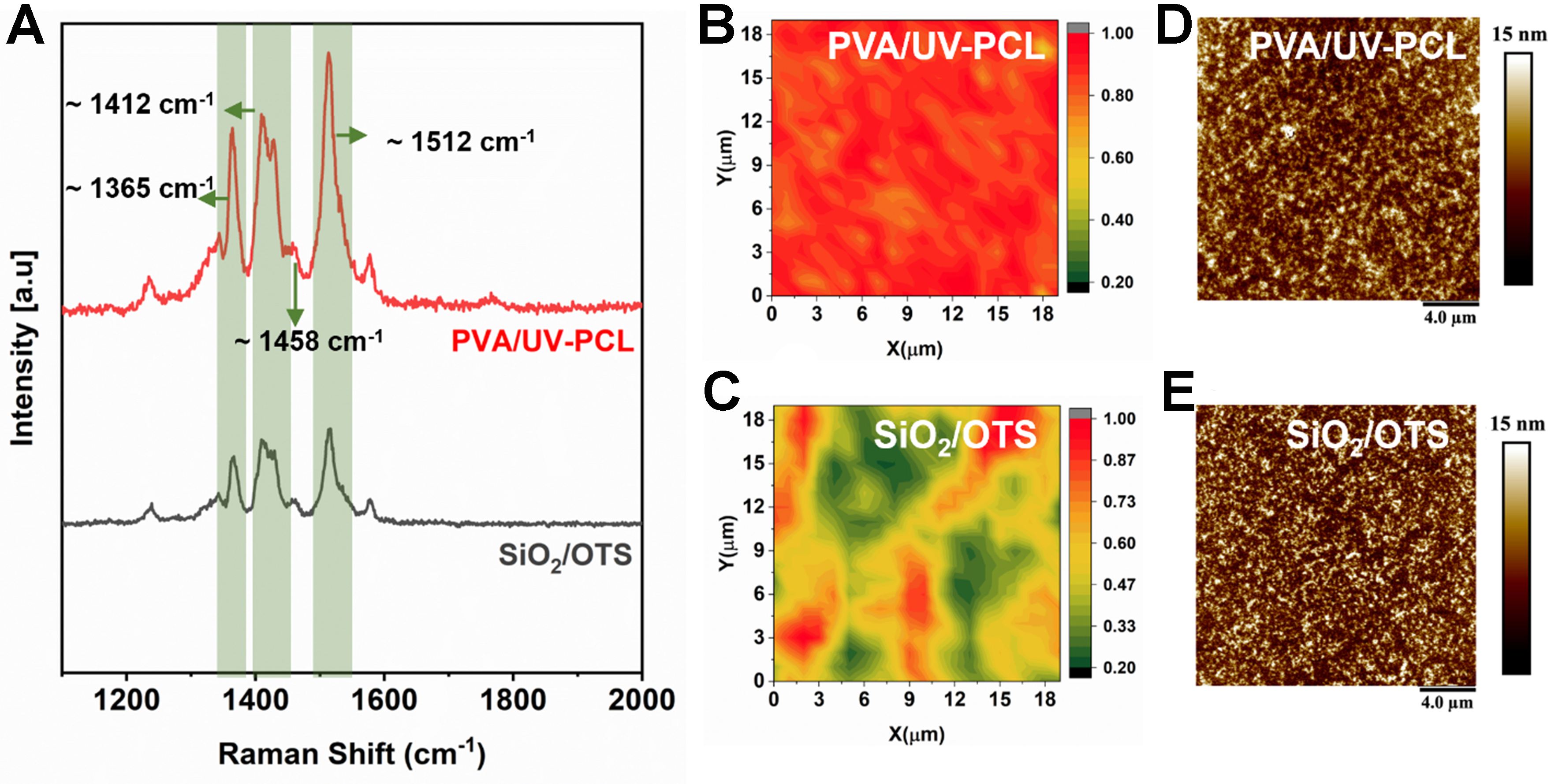
Figure 4. Raman spectra (A) and maps (19 × 19 µm2) (B and C) of degradable P(DPP-TIT) semiconductor on bilayer dielectric (PVA/UV-PCL) and OTS-treated SiO2. 20 × 20 μm AFM topography images of thin films of P(DPP-TIT) deposited on (D) the degradable polymer dielectric and (E) OTS-treated SiO2. P(DPP-TIT): Poly diketopyrrolopyrrole thiophene-imine-thiophene; PVA: poly(vinyl alcohol); UV: ultraviolet; PCL: poly(caprolactone); OTS: octyltrichlorosilane; AFM: atomic force microscopy.