


fig5
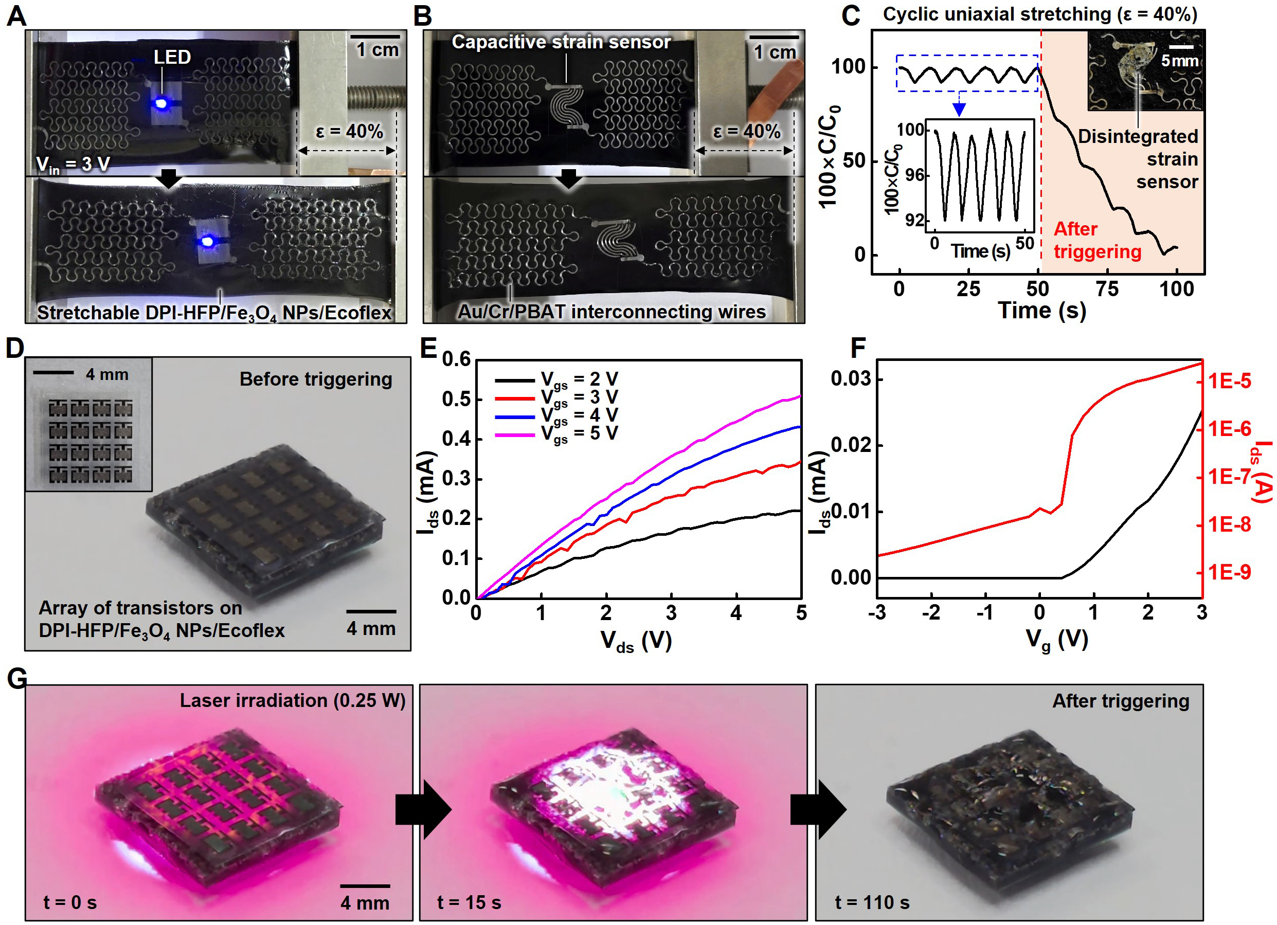
Figure 5. Laser-triggered transient electronics on stretchable DPI-HFP/Fe3O4 NPs/Ecoflex 00-30 substrate. Images of (A) a blue LED and (B) an interdigitated capacitive strain sensor connected to serpentine interconnecting wires composed of Au (~ 75 nm)/Cr (~ 15 nm)/PBAT (~ 30 µm), integrated on a stretchable DPI-HFP (10 wt.%)/Fe3O4 NPs (1.00 wt.%)/Ecoflex 00-30 substrate (~ 220 µm), before (top) and after (bottom) uniaxial stretching (uniaxial strain = 40 %). In the top view, the interconnecting wires appear light gray due to the Cr layer beneath the transparent PBAT layer, which covers the underlying Au layer directly interfaced with the composite substrate; (C) Capacitance change of the strain sensor before and after laser triggering in the middle of 10 cycles of uniaxial stretching at 40% strain (strain rate = 8% s-1). A 0.25 W laser was irradiated after the fifth cycle; (D) Images showing a 4 × 4 array of n-channel MOSFETs composed of Si NMs (~ 400 nm), SiO2 gate dielectric (~ 100 nm), Mo electrodes (~ 400 nm), and PBAT top layer (~ 30 µm) integrated on a DPI-HFP/Fe3O4 NPs/Ecoflex substrate. The inset shows a top view of the MOSFET array before integration onto the composite substrate; (E) I-V curve and (F) transfer curve of an n-channel MOSFET on the composite substrate; (G) Images showing the MOSFET array during (left and middle) and after (right) the 800 nm laser irradiation (spot size = 8 mm (diameter), pulse width = ~ 100 fs, power = 0.25 W) for 110 s. LED: Light-emitting diode; PBAT: polybutylene adipate terephthalate; NP: nanoparticle; DPI-HFP: diphenyliodonium hexafluorophosphate; MOSFET: metal-oxide-semiconductor field-effect transistor; NM: nanomembrane.