fig2
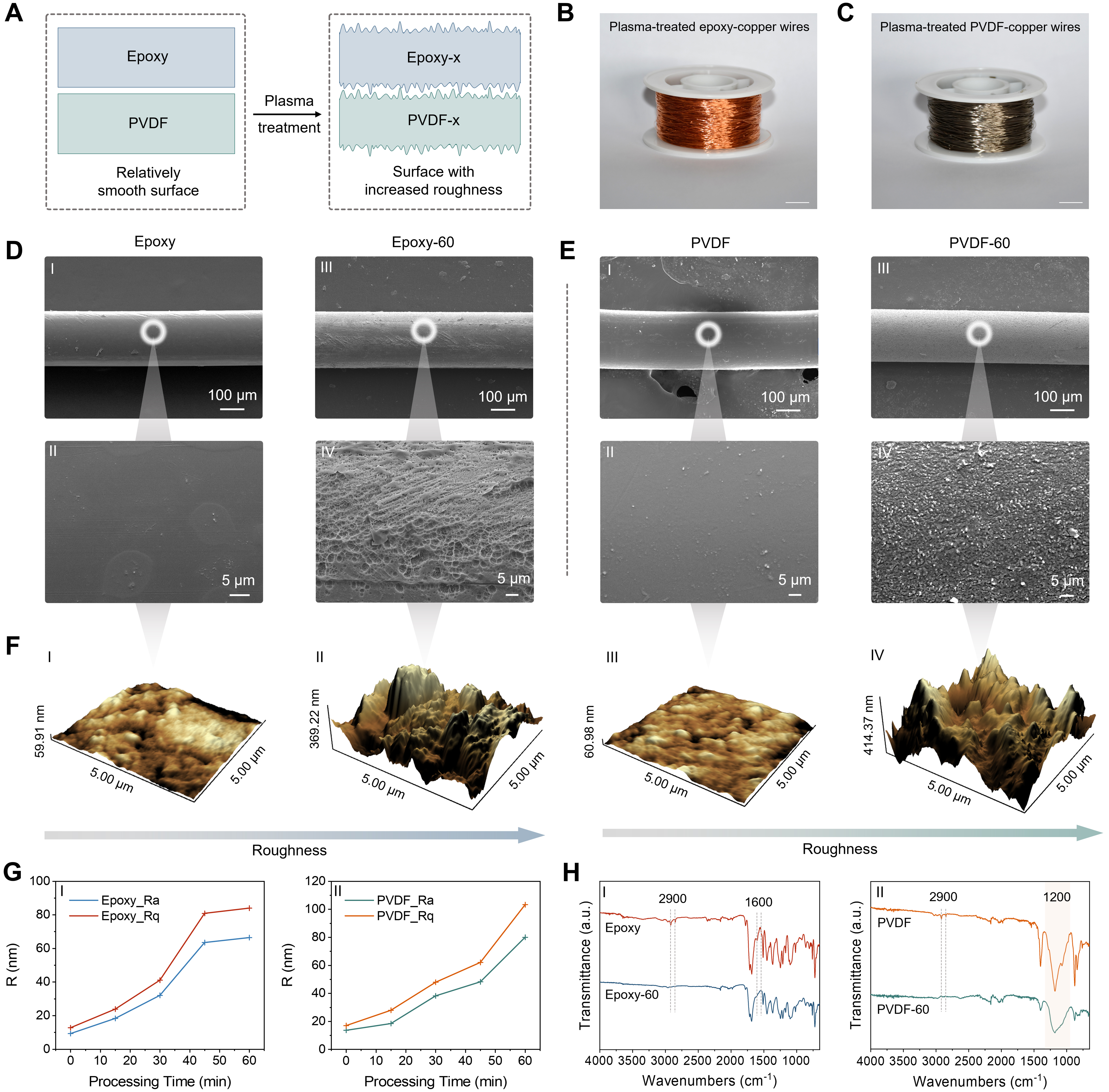
Figure 2. Characterization of the surface treatment of triboelectric fibers. (A) Schematic illustration of the fiber surfaces before and after plasma treatment. Digital images of surface-treated (B) epoxy-coated and (C) PVDF-coated copper wires with a diameter of 200 μm (Scale bar: 10 mm); (D) and (E) SEM images, and (F) 3D AFM images of epoxy and PVDF fibers before and after 60-minute plasma treatment, respectively; (G) Roughness variation of 5 μm × 5 μm surface regions for epoxy and PVDF fibers with plasma treatment time at varying durations; (H) FTIR spectra of epoxy and PVDF fibers before and after plasma treatment. PVDF: Polyvinylidene fluoride; SEM: scanning electron microscope; 3D: three-dimensional; AFM: atomic force microscopy; FTIR: Fourier Transform Infrared.


