


Defect-induced interfacial modulation for enhanced resistive switching performance in antiferroelectric/ferroelectric heterostructures

 ,
, Abstract
Resistive switching devices, particularly memristors, have attracted considerable interest due to their promising applications in neuromorphic computing and data storage. However, achieving high performance and reliability remains a significant challenge, especially in the optimization of their ferroelectric and switching properties. In this study, we report a substantial enhancement of both resistive switching and ferroelectric properties in NaNbO3 (NNO)/PbTiO3 (PTO) multilayers, facilitated by interfacial modifications of the electronic structure induced by defects and strain. The well-defined interfaces and strain gradients within the PTO layers lead to substantial alterations in local electronic properties, including Ti 3d orbital hybridization and oxygen octahedral tilting. These structural modifications enhance charge trapping dynamics, resulting in an ON/OFF ratio of 104, compared with 102 in single-layer NNO films. The synergistic effects of enhanced polarization and electronic state modulation are shown to optimize both the ferroelectric and resistive switching behaviors, highlighting the pivotal role of interface engineering in achieving high-performance memristive devices.

Keywords
INTRODUCTION
With the arrival of the 5G era and the rapid development of technologies such as artificial intelligence (AI) and big data, the requirements for information storage and data processing have become increasingly stringent, placing unprecedented demands on the performance of semiconductor memory[1-5]. A memristor is a nonlinear resistor with memory capabilities, enabling non-volatile multistate storage and finding widespread application in neuromorphic computing[6]. However, traditional memristors often suffer from poor storage stability, presenting significant challenges for use in information processing and artificial synapses. As a result, there has been growing interest in the development of advanced, flexible memristors. Among the various emerging memory devices, ferroelectric memristors, operating based on the reversal of ferroelectric polarization, have shown great promise, offering stable non-volatile information storage[7-10]. By integrating ferroelectric memristors with flexible substrates, flexible ferroelectric memristors can be developed and provide a range of advantages including low power consumption, high storage density, enhanced bend resistance, etc. These devices hold great merits for constructing artificial synaptic systems in neuromorphic computing, unlocking significant potential for new flexible information devices in the field of AI. For instance, Xue et al. demonstrated that the emerging van der Waals ferroelectric material
The performance of ferroelectric memristors is mainly characterized by the ON/OFF ratio, operating speed, data storage capacity, and power consumption[13-16]. These fundamental properties are influenced not only by the magnitude of ferroelectric polarization but also by the spontaneous ferroelectric domain structure and its switching dynamics[17,18]. In recent years, various methods have been proposed to control the domain structure of ferroelectric thin films, including bandgap regulation[19], strain engineering[20], defect engineering[21-23] and interface engineering[24-26]. However, relying on a single approach often fails to yield optimal results. In comparison, Jeon et al. demonstrated that the synergistic effects of strain engineering and bending electric fields could effectively modulate domain configurations in BiFeO3 (BFO), facilitating the creation of ferroelectric diodes with enhanced resistive switching properties[27]. This demonstrates that combining multiple control methods can induce coupling between various order parameters, generating a complex set of factors that influence the configuration of ferroelectric domain structures. Factors such as the charge screening ability of electrodes[28], the electrostatic coupling between defect dipoles and polarization[29], and the interfacial band mismatch[30], have all been shown to play critical roles in tailoring the self-polarization state. Despite these advances, achieving controlled multiscale regulation of domain configurations via interface-induced methods remains a significant challenge, and the impact of such regulation on the performance of resistive switching devices is not yet fully understood.
NaNbO3 (NNO) has attracted significant interest due to their promising ferro- and piezoelectric properties and is, thus, considered a possible candidate to replace hazardous lead-based materials in piezo-/ferroelectric technological devices[31,32]. Its ability to undergo defect formation, particularly the generation of columnar defects such as antisite and Nb5+-related defects, provides a valuable tool for tuning the electronic and ferroelectric properties. These defects can introduce local strain and modify the electronic structure at the interface, thereby improving device performance. On the other hand, PbTiO3 (PTO) is a well-established ferroelectric material with strong polarization characteristics, high Curie temperature, and excellent ferroelectric switching properties, which are crucial for the functioning of ferroelectric devices[33-35]. When integrated with NNO, ferroelectric properties of PTO can be enhanced by the electronic conductivity of NNO, making the NNO/PTO multilayer an ideal candidate for achieving superior resistive switching and polarization coupling.
In this study, we investigate the (NNO/PTO)3 (NNO/PTO) multilayer heterostructure as a model system, combining the excellent metallic conductivity and oxygen ion mobility of NNO with the robust ferroelectricity and polarization tunability of PTO. These complementary properties make the NNO/PTO system an ideal platform for exploring the interfacial effects on resistive switching and ferroelectric behavior. We examine how defect-induced interfacial strain and lattice distortions influence the electronic structure and polarization coupling in NNO/PTO multilayers. Using advanced transmission electron microscopy (TEM) techniques, such as high-resolution high-angle annular dark-field scanning TEM (HAADF-STEM), geometric phase analysis (GPA), and electron energy loss spectroscopy (EELS), we reveal the critical role of oxygen octahedral distortions and orbital hybridization at the interface. These findings provide valuable insights into the mechanisms behind the enhanced ON/OFF resistive switching ratio (104) and improved polarization, paving the way for the design of high-performance resistive switching devices through precise interface engineering.
METHODS
Film growth and basic characterization
NNO and NNO/PTO multilayer films were grown on Nb-STO single-crystal substrates using pulsed laser deposition (PLD). The target materials used were commercially available NNO and PTO. Growth was carried out at a substrate temperature of 750 °C under an oxygen partial pressure of 70 mTorr. The laser energy density was maintained at 1.5 J/cm2, and the pulse repetition rate was 5 Hz. After the deposition, the temperature was cooled to 25 °C with an oxygen atmosphere of 200 Torr. The cooling rate is 5 °C/min. The crystallographic structure and phase purity of the films were examined by high-resolution X-ray diffraction (HRXRD) using a Bruker D8 Discover diffractometer. θ-2θ scans were conducted to confirm film quality, orientation, and phase formation.
Atomic-scale structural characterization
Aberration-corrected TEM was employed to investigate the local atomic structure. TEM analysis was performed using a Titan Themis microscope operated at 300 kV equipped with a probe corrector (CEOS, Gmbh). For the HAADF-STEM imaging, we adopted a probe size of < 1 Å. The convergent semi-angle and the collection semi-angle are 21.4 mrad and 37-200 mrad, respectively. Meanwhile, the spatial resolution was 60 pm. Energy-dispersive X-ray spectroscopy (EDS) and EELS were performed to analyze elemental composition and provide detailed chemical insights, particularly focusing on Ti 3d orbital hybridization and oxygen vacancy distribution. EELS of O-K and Ti-L2,3 was acquired with an energy resolution of 0.8 eV (determined by the full width of a zero-loss peak at half maximum) and a dispersion of 0.05 eV/ch. The entrance aperture was selected to be 5 mm. Two-dimensional Gaussian fitting of the HAADF-STEM images was performed using Matlab software to accurately determine the positions of the atomic columns.
Piezoresponse force microscopy and resistive switching measurements
Piezoresponse force microscopy (PFM) was used to investigate domain configurations and reversal behavior under an applied electric field. Measurements were conducted on an Asylum Research Cypher S atomic force microscope (AFM), and the domain dynamics were observed under bipolar voltage pulses
RESULTS AND DISCUSSION
We successfully fabricated single-layer NNO thin films and three-period NNO/PTO multilayer films on Nb-doped SrTiO3 (Nb-STO) (001) substrates using PLD. The thicknesses of the individual NNO and PTO layers in the multilayer structure were 20 and 10 nm, respectively. Figure 1A shows the HRXRD pattern of the single-layer NNO epitaxial film. The sharp and well-defined diffraction peaks indicate high crystallinity and excellent epitaxial alignment with the substrate. No secondary phases were detected, confirming the successful growth of a pure NNO film. Figure 1B presents the XRD patterns of the three-period NNO/PTO multilayer films.
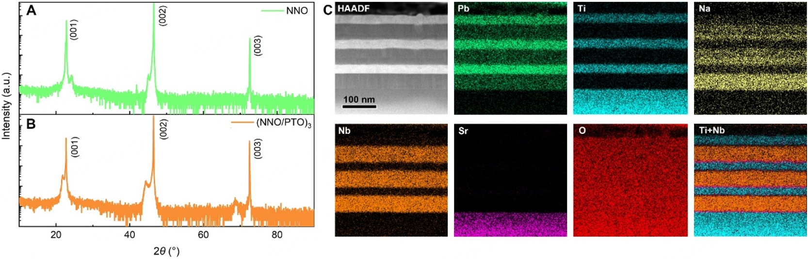
Figure 1. Crystal structure characterization of epitaxial NNO and (NNO/PTO)3 thin films. Out-of-plane XRD θ-2θ scans of NNO thin films (A) and (NNO/PTO)3. (B) grown on (001) Nb-STO substrates. (C) Low-magnification HAADF-STEM image of the (NNO/PTO)3 film grown on Nb-STO substrates and EDS mapping of the (NNO/PTO)3/Nb-STO heterointerface.
Figure 1C shows the EDS mapping of the three-period NNO/PTO multilayer. The uniform spatial distribution of Na, Nb, Pb, and Ti elements confirms the compositional homogeneity within each layer. Additionally, no significant elemental interdiffusion was observed at the interfaces, indicating sharp and well-defined boundaries between the NNO and PTO layers. These results highlight the successful fabrication of high-quality NNO/PTO multilayers with precise periodicity and well-defined interfaces, which are essential for the intended functionalities of the heterostructure.
The ferroelectric and resistive switching properties of the single-layer NNO and NNO/PTO multilayer films were systematically investigated, as shown in Figure 2. Figure 2A and B presents the PFM phase-switching mappings for the single-layer NNO film and the NNO/PTO multilayer film, respectively. In both cases, a clear 180° phase reversal is observed within the written domains, demonstrating robust ferroelectric switching behavior. To further confirm the phase reversal, Figure 2C shows the phase profile across the switched regions, revealing a distinct 180° phase difference. Notably, the phase contrast is more pronounced in the multilayer film compared with the single-layer film, suggesting enhanced ferroelectric behavior due to interfacial interactions within the multilayer structure. The stable polarization state accounts for the minimal cycle and device variations, which are crucial for improving the performance of resistive switching devices. Additionally, local PFM hysteresis behavior, including the 180° phase reversal and the characteristic “butterfly-shaped” amplitude curves, further confirms the ferroelectric switching
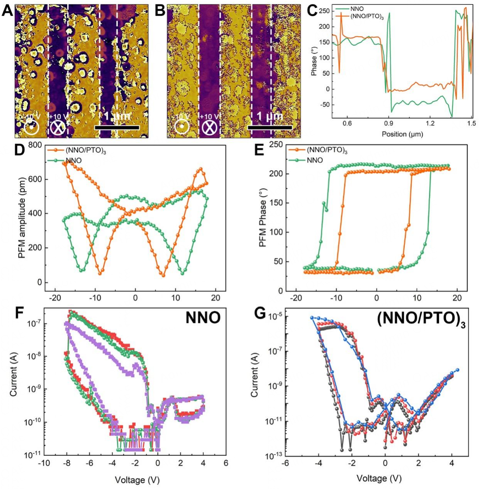
Figure 2. Scanning probe microscopy characterization and nonvolatile resistive switching of Nb-STO/(NNO/PTO)3/Au memristors. (A and B) PFM phase images with square domain patterns written by +10 V and -10 V for NNO and (NNO/PTO)3 film, respectively. (C) Position dependent phase changes along the while lines in (A and B), respectively. (D and E) Amplitude curves (D) and phase switching spectroscopy loops (E) collected with the cantilever for NNO and (NNO/PTO)3 films. (F and G) I-V characteristics for (F) NNO and (G) (NNO/PTO)3 devices.
To evaluate the stability and reliability of the resistive switching behavior, we conducted fatigue and retention tests on the NNO/PTO multilayer devices. Figure 3A shows the fatigue performance, where the device undergoes repeated switching cycles. The results demonstrate excellent endurance, with no significant degradation in the ON/OFF ratio after up to 105 cycles, indicating that the device maintains stable switching performance over extended operation periods. This suggests that the resistive switching mechanism is highly reliable, with minimal impact from cycling fatigue. Additionally, the retention characteristics of the device were assessed and are presented in Figure 3B. The retention test was conducted by measuring the resistance of the device in both the HRS and LRS over a period of 103 s. The results show that both states remain stable, with no noticeable drift in resistance, confirming the excellent retention capability of the device. This long-term stability further highlights the potential of the NNO/PTO multilayer as a promising candidate for non-volatile memory applications.

Figure 3. Fatigue and retention characteristics for (NNO/PTO)3. (A) Fatigue properties of the HRS and LRS for (NNO/PTO)3. (B) Retention properties of the HRS and LRS with a pulse width of 1 s for (NNO/PTO)3.
To gain insight into the origin of the enhanced performance in the NNO/PTO multilayers, we conducted atomic-scale characterization of the interface region. Figure 4A presents a low-magnification HAADF-STEM image of the three-period NNO/PTO multilayer, clearly revealing the periodicity of the NNO and PTO layers and confirming the successful growth of the multilayer structure. Figure 4B provides a magnified view of the interface region (marked by the orange box), where the interfacial coherence between the NNO and PTO layers is evident. The sharpness of the interface indicates minimal interdiffusion, which is crucial for preserving the desired material properties. Then, we found a vertically aligned nanopillar in the cross-sectional view of NNO [Figure 4C]. The nanopillar is embedded in the matrix of a regular perovskite structure. Inside the nanopillar regions, the Nb atoms occupy the original Na positions along both in-plane directions, and the Na atoms also occupy the original Nb positions along both in-plane directions. This kind of antisite NbNa defect is typical in the NNO perovskite oxides. The atomic-level EDS analysis shown in Figure 4D reveals the distribution of elements across the interface, with concentration profiles indicating a well-defined boundary between the NNO and PTO layers, and no significant elemental intermixing at the interface. This sharp interface is likely responsible for the improved charge transport and resistive switching behavior observed in the multilayer. Finally, Figure 4E displays the polarization distribution in the PTO layer near the interface. A significant enhancement of polarization is observed near the NNO/PTO interface, attributed to interfacial strain and defect-induced effects. Moreover, interfacial antisite defects help stabilize the single domain in PTO, potentially resulting in a gradient distribution of oxygen vacancies. The significant enhancement of polarization near the NNO/PTO interface can be attributed to the interplay between the interfacial strain and the polarization of the PTO layer. The presence of defects and strain at the NNO/PTO interface influences the local lattice structure of PTO, resulting in an increased polarization near the interface. This enhancement is due to the modification of the oxygen octahedral tilting and the strain-induced distortion in the PTO layer, which stabilizes the ferroelectric dipoles and enhances the local polarization. The comparative explanation between the interface region and the bulk region of the PTO layer reveals that while the bulk exhibits a relatively uniform polarization distribution, the interface region shows a much stronger polarization response. This is likely due to the strain-induced polarization coupling between the NNO and PTO layers, which significantly alters the local polar orientation and strengthens the overall polarization in the interface region. This may explain the memristive behavior, with an outstanding ON/OFF ratio of 104. The strong polarization at the interface is believed to play a critical role in enhancing resistive switching performance by facilitating charge trapping processes, which are key to the resistive switching mechanism.
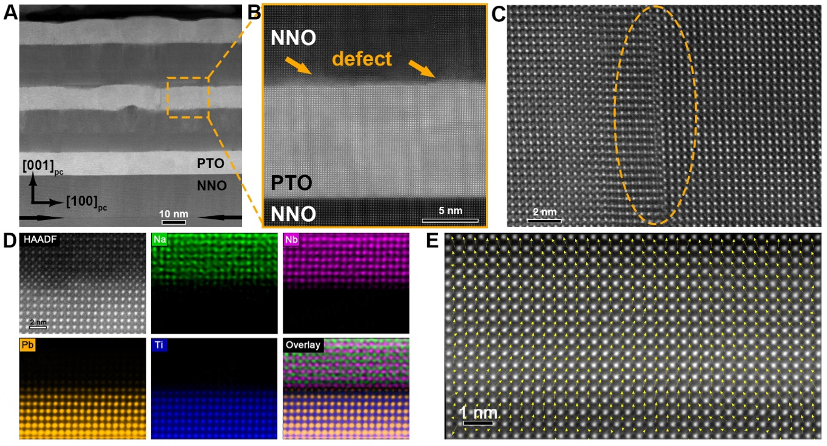
Figure 4. Structure and element analysis of NNO/PTO thin films grown on Nb-STO substrates. (A) Low-magnification HAADF-STEM image of (NNO/PTO)3 thin films and (B) enlarged image of the NNO/PTO interface marked by orange box in (A). (C) Cross-sectional atomically resolved HAADF image of NNO. Antisite NbNa defects can be clearly observed. (D) Atomic HAADF-STEM image and EDS mapping of the NNO/PTO heterointerface. (E) The enlarged atomic positions together with the atomic displacement mapping of Ti ions (yellow arrows) of typical regions near and away from the NNO/BTO interface.
The resistive switching phenomenon can be explained through mechanisms such as charge migration, defect-induced local electric fields, and ion movement. Under an applied electric field, electrons or ions in the material migrate, leading to local changes in the electric field and thus altering the material resistance. Specifically, under a positive electric field, oxygen vacancies or metal ions migrate toward the electrode, leading to an increase in local conductivity; under a negative electric field, these ions or defects migrate back or redistribute, restoring the initial HRS. By adjusting parameters such as field strength and pulse width, the resistance state of the material can be precisely controlled, enabling information storage and retrieval.
The resistive switching in ferroelectric materials can be understood in terms of the interaction between the ferroelectric polarization and the local electric field at the interface. When a voltage is applied across a ferroelectric material, the polarization of the ferroelectric layer aligns with the electric field, causing a redistribution of charge carriers at the interface. This results in a significant variation in the electric field at the interface, which in turn affects the resistance of the material. The resistance can either increase or decrease depending on the direction of the applied voltage and the polarization state of the ferroelectric layer. In the "set" process (switching from HRS to LRS), the applied voltage causes the polarization to switch direction, which induces charge redistribution that reduces the resistance. Conversely, during the "reset" process (switching from LRS to HRS), the polarization is reversed, and the resistance increases.
The presence of defects, such as oxygen vacancies or metal ion migration, also significantly contributes to the resistive switching behavior in ferroelectric devices. These defects can modify the local electric field, leading to changes in the resistance of the device. For example, oxygen vacancies may migrate under an applied field, creating localized conductive paths that facilitate the LRS. In ferroelectric materials, the defects interact with the polarization, which can modulate the resistance switching characteristics by altering the interface properties. In addition to defects, the interface between the ferroelectric layer and the electrodes is crucial for resistive switching. The interface can significantly influence the voltage threshold and the switching dynamics due to the formation of depletion or accumulation regions at the interface. These regions can affect the ion migration and the distribution of charge carriers, further impacting the resistive switching behavior of devices.
To further investigate the atomic-scale mechanisms underlying the enhanced performance of the NNO/PTO multilayer, we performed GPA and EELS near the interface. Figure 5A presents a HAADF-STEM image of the NNO/PTO multilayer, where the atomic arrangement and periodicity of the layers are clearly visible. Figure 5B and C shows the in-plane and out-of-plane strain maps derived from GPA. The strain maps reveal a significant strain gradient in the out-of-plane direction near the interface, with a marked increase in strains at the PTO layer adjacent to the NNO/PTO interface. This observation suggests that antisite defects at the interface play a key role in modulating the strain distribution within the PTO layer, which can influence the local electronic structure and ferroelectric properties. The large out-of-plane strain near the interface is expected to promote polarization enhancement and contribute to improved resistive switching performance. Figure 5D shows the Ti-L and O-K EELS spectra from the interface region. The Ti

Figure 5. Atomic-scale STEM and EELS analysis of the (NNO/PTO)3 thin films. (A) Cross-sectional HAADF-STEM image of the (NNO/PTO)3 film. (B) IP strain εxx and (C) OOP strain εyy mappings from the corresponding HAADF-STEM image shown in (A) using GPA. Bar = 10 nm. (D) EELS Ti-L and O-K edges of the scanning range from the inside to the interface in the PTO.
The resistive switching behavior in NNO/PTO multilayers is driven by the synergistic effects of interface strain and polarization coupling. Oxygen vacancies, as a crucial factor influencing memristive devices, are redistributed through interface engineering and defect modulation, which in turn affects the barrier height at the material interface and consequently regulates the macroscopic electrical properties of the material. Additionally, oxygen vacancies, primarily in the NNO layer, play a key role in modulating the local resistance under an applied electric field. As vacancies migrate and accumulate at the interface, they alter the electronic structure, facilitating the transition between the HRS and LRS. This process is further influenced by the strain at the NNO/PTO interface, which results from the lattice mismatch between the two materials. The strain not only affects the polarization of the PTO layer but also alters the local charge distribution, promoting enhanced resistive switching. The polarization coupling between NNO and PTO at the interface further stabilizes the high and low resistance states, contributing to the observed high ON/OFF ratio. The modified electronic structure at the interface, as revealed by techniques such as EELS and GPA, shows that oxygen vacancies and strain significantly alter the local electronic states, creating localized states near the Fermi level that facilitate charge trapping dynamics. This leads to improved switching stability and speed, making the NNO/PTO multilayer a promising candidate for non-volatile memory applications. These results highlight the critical role of defect engineering and interface modulation in achieving high-performance resistive switching, offering a pathway for future device optimization through further exploration of interface effects, defect density, and material composition.
CONCLUSION
In conclusion, our study demonstrates that the enhanced resistive switching and ferroelectric properties in NNO/PTO multilayers are primarily driven by interfacial electronic structure modifications induced by antisite defects and strain. The well-defined interface and strain gradient within the PTO layers significantly alter the local electronic structure, particularly the Ti 3d orbital hybridization and oxygen octahedral tilting, as revealed by EELS and GPA. These changes enhance charge trapping dynamics, leading to a marked improvement in resistive switching performance, with the multilayer exhibiting an ON/OFF ratio of 104, compared with 102 in the single-layer NNO film. Additionally, the enhanced polarization near the interface, along with the modulation of electronic states, plays a crucial role in optimizing both the ferroelectric and resistive switching behaviors. This work underscores the importance of interface engineering in controlling electronic structure to achieve high-performance resistive switching devices and provides valuable insights for future device optimization.
DECLARATIONS
Authors’ contributions
Design, manuscript revision and supervision: Zhu, Y. L.; Ma, X. L.
Experiments and data collection: Liu, J. Q.; Zhu, H. L.; Liu, F.; Shi, T. T.
Data analysis: Liu, J. Q.; Yang, L. X.; Tang, Y. L.; Xu, G.; Ma, J. Y.; Shi, T. T.; Wang, Y. J.
Manuscript writing: Liu, J. Q.; Zhu, H. L.
All authors have read and agreed to the published version of the manuscript.
Availability of data and materials
The data that support the findings of this study are available from the corresponding author upon reasonable request.
Financial support and sponsorship
This work is supported by the National Natural Science Foundation of China (no. 52122101, no. 51971223), Guangdong Provincial Quantum Science Strategic Initiative (no. GDZX2202001, GDZX2302001) and Shenyang National Laboratory for Materials Science (L2022R04, L2021F06); The Youth Innovation Promotion Association CAS (no. 2021187), The Scientific Instrument Developing Project of CAS (YJKYYQ20200066) and the Youth Innovation Promotion Association of CAS (Y202048); The National Natural Science Foundation of China (Grant No. 52161003).
Conflicts of interest
Tang, Y. L. is the Guest Editor of the Special Issue “Role of Microstructures in the High-performance of Advanced Dielectric Materials and Devices” but was not involved in any steps of editorial processing, notably including reviewer selection, manuscript handling, or decision-making, while the other authors have declared that they have no conflicts of interest.
Ethical approval and consent to participate
Not applicable.
Consent for publication
Not applicable.
Copyright
© The Author(s) 2025.
REFERENCES
1. Yoon, D. S.; Roh, J. S.; Lee, S. M.; Baik, H. K. Alteration for a diffusion barrier design concept in future high-density dynamic and ferroelectric random access memory devices. Prog. Mater. Sci. 2003, 48, 275-371.
2. Chang, T. C.; Chang, K. C.; Tsai, T. M.; Chu, T. J.; Sze, S. M. Resistance random access memory. Mater. Today. 2016, 19, 254-64.
3. Kim, I. J.; Lee, J. S. Ferroelectric transistors for memory and neuromorphic device applications. Adv. Mater. 2023, 35, e2206864.
4. Kim, S. S.; Yong, S. K.; Kim, W.; et al. Review of semiconductor flash memory devices for material and process issues. Adv. Mater. 2023, 35, e2200659.
5. Migliato, M. G.; Zhao, Y.; Avsar, A.; et al. Logic-in-memory based on an atomically thin semiconductor. Nature 2020, 587, 72-7.
6. Zhao, M.; Gao, B.; Tang, J.; Qian, H.; Wu, H. Reliability of analog resistive switching memory for neuromorphic computing. App. Phys. Rev. 2020, 7, 011301.
7. Li, X.; Liu, J.; Huang, J.; et al. Epitaxial strain enhanced ferroelectric polarization toward a giant tunneling electroresistance. ACS. Nano. 2024, 18, 7989-8001.
8. Li, Y. Z.; Lin, J. L.; Bai, Y.; Li, Y.; Zhang, Z. D.; Wang, Z. J. Ultrahigh-energy storage properties of (PbCa)ZrO3 antiferroelectric thin films via constructing a pyrochlore nanocrystalline structure. ACS. Nano. 2020, 14, 6857-65.
9. Tang, Y. L.; Zhu, Y. L.; Ma, X. L.; et al. Observation of a periodic array of flux-closure quadrants in strained ferroelectric PbTiO3 films. Science 2015, 348, 547-51.
10. Wang, Y. J.; Feng, Y. P.; Zhu, Y. L.; et al. Polar meron lattice in strained oxide ferroelectrics. Nat. Mater. 2020, 19, 881-6.
11. Xue, F.; He, X.; Wang, Z.; et al. Giant ferroelectric resistance switching controlled by a modulatory terminal for low-power neuromorphic in-memory computing. Adv. Mater. 2021, 33, e2008709.
12. Luo, Z.; Wang, Z.; Guan, Z.; et al. High-precision and linear weight updates by subnanosecond pulses in ferroelectric tunnel junction for neuro-inspired computing. Nat. Commun. 2022, 13, 699.
13. Yan, X.; Yan, H.; Liu, G.; et al. Silicon-based epitaxial ferroelectric memristor for high temperature operation in self-assembled vertically aligned BaTiO3-CeO2 films. Nano. Res. 2022, 15, 9654-62.
14. Molinari, A.; Witte, R.; Neelisetty, K. K.; et al. Configurable resistive response in BaTiO3 ferroelectric memristors via electron beam radiation. Adv. Mater. 2020, 32, e1907541.
15. McConville, J. P. V.; Lu, H.; Wang, B.; et al. Ferroelectric domain wall memristor. Adv. Funct. Mater. 2020, 30, 2000109.
16. Ma, C.; Luo, Z.; Huang, W.; et al. Sub-nanosecond memristor based on ferroelectric tunnel junction. Nat. Commun. 2020, 11, 1439.
17. Gabel, M.; Gu, Y. Understanding microscopic operating mechanisms of a van der Waals planar ferroelectric memristor. Adv. Funct. Mater. 2021, 31, 2009999.
18. Müller, M. L.; Becker, M. T.; Strkalj, N.; Macmanus-driscoll, J. L. Schottky-to-ohmic switching in ferroelectric memristors based on semiconducting Hf0.93Y0.07O2 thin films. Appl. Phys. Lett. 2022, 121, 093501.
19. Yang, F.; Bao, Y.; Huang, W.; Li, X.; Chen, Y.; Wang, G. Enhanced energy storage properties of hafnium-modified
20. Tang, Y.; Zhu, Y.; Wu, B.; et al. Periodic polarization waves in a strained, highly polar ultrathin SrTiO3. Nano. Lett. 2021, 21, 6274-81.
21. Mcgilly, L. J.; Sandu, C. S.; Feigl, L.; Damjanovic, D.; Setter, N. Nanoscale defect engineering and the resulting effects on domain wall dynamics in ferroelectric thin films. Adv. Funct. Mater. 2017, 27, 1605196.
22. Gradauskaite, E.; Hunnestad, K. A.; Meier, Q. N.; Meier, D.; Trassin, M. Ferroelectric domain engineering using structural defect ordering. Chem. Mater. 2022, 34, 6468-75.
23. Nataf, G. F.; Guennou, M.; Gregg, J. M.; et al. Domain-wall engineering and topological defects in ferroelectric and ferroelastic materials. Nat. Rev. Phys. 2020, 2, 634-48.
24. Li, C.; Huang, L.; Li, T.; et al. Ultrathin BaTiO3-based ferroelectric tunnel junctions through interface engineering. Nano. Lett. 2015, 15, 2568-73.
25. Guo, R.; Zhou, Y.; Wu, L.; et al. Control of synaptic plasticity learning of ferroelectric tunnel memristor by nanoscale interface engineering. ACS. Appl. Mater. Interfaces. 2018, 10, 12862-9.
26. Chen, D.; Chen, Z.; He, Q.; et al. Interface engineering of domain structures in BiFeO3 thin films. Nano. Lett. 2017, 17, 486-93.
27. Jeon, B. C.; Lee, D.; Lee, M. H.; et al. Flexoelectric effect in the reversal of self-polarization and associated changes in the electronic functional properties of BiFeO3 thin films. Adv. Mater. 2013, 25, 5643-9.
28. Chu, Y. H.; He, Q.; Yang, C. H.; et al. Nanoscale control of domain architectures in BiFeO3 thin films. Nano. Lett. 2009, 9, 1726-30.
29. Lee, D.; Jeon, B. C.; Baek, S. H.; et al. Active control of ferroelectric switching using defect-dipole engineering. Adv. Mater. 2012, 24, 6490-5.
30. Huang, B.; Zhao, X.; Li, X.; et al. Schottky barrier control of self-polarization for a colossal ferroelectric resistive switching. ACS. Nano. 2023, 17, 12347-57.
31. Singh, S.; Khare, N. Electrically tuned photoelectrochemical properties of ferroelectric nanostructure NaNbO3 films. Appl. Phys. Lett. 2017, 110, 152902.
32. Jung, J. H.; Lee, M.; Hong, J. I.; et al. Lead-free NaNbO3 nanowires for a high output piezoelectric nanogenerator. ACS. Nano. 2011, 5, 10041-6.
33. Li, S.; Zhu, Y.; Tang, Y.; et al. Thickness-dependent a/a domain evolution in ferroelectric PbTiO3 films. Acta. Mater. 2017, 131, 123-30.
34. Tang, Y.; Zhu, Y.; Ma, X.; et al. A coherently strained monoclinic [111]PbTiO3 film exhibiting zero poisson’s ratio state. Adv. Funct. Mater. 2019, 29, 1901687.
35. Chen, Y. T.; Tang, Y. L.; Zhu, Y. L.; et al. Periodic vortex-antivortex pairs in tensile strained PbTiO3 films. Appl. Phys. Lett. 2020, 117, 192901.
36. Zheng, N.; Zang, Y.; Li, J.; et al. Perovskite-oxide-based ferroelectric synapses integrated on silicon. Adv. Funct. Mater. 2024, 34, 2316473.
Cite This Article
 , ... Xiu-Liang Ma
How to Cite
Download Citation
Export Citation File:
Type of Import
Tips on Downloading Citation
Citation Manager File Format
Type of Import
Direct Import: When the Direct Import option is selected (the default state), a dialogue box will give you the option to Save or Open the downloaded citation data. Choosing Open will either launch your citation manager or give you a choice of applications with which to use the metadata. The Save option saves the file locally for later use.
Indirect Import: When the Indirect Import option is selected, the metadata is displayed and may be copied and pasted as needed.
About This Article
Special Topic
Copyright


Comments
Comments must be written in English. Spam, offensive content, impersonation, and private information will not be permitted. If any comment is reported and identified as inappropriate content by OAE staff, the comment will be removed without notice. If you have any queries or need any help, please contact us at [email protected].