fig1

Defect-induced interfacial modulation for enhanced resistive switching performance in antiferroelectric/ferroelectric heterostructures

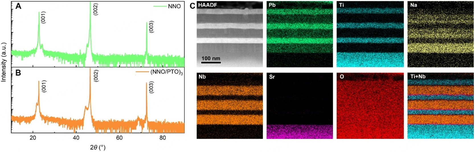
Figure 1. Crystal structure characterization of epitaxial NNO and (NNO/PTO)3 thin films. Out-of-plane XRD θ-2θ scans of NNO thin films (A) and (NNO/PTO)3. (B) grown on (001) Nb-STO substrates. (C) Low-magnification HAADF-STEM image of the (NNO/PTO)3 film grown on Nb-STO substrates and EDS mapping of the (NNO/PTO)3/Nb-STO heterointerface.

Microstructures
ISSN 2770-2995 (Online)

Portico

All published articles are preserved here permanently:

https://www.portico.org/publishers/oae/

Portico

All published articles are preserved here permanently:

https://www.portico.org/publishers/oae/