


The influence of A/B-sites doping on antiferroelectricity of PZO energy storage films

 ,
,
Abstract
Antiferroelectrics are a kind of unique dielectric materials, mainly due to their polarization behavior, and composition-induced antiferroelectricity stability also draws considerable attention. In this work, single orthorhombic phase (Pb0.95Bi0.05)ZrO3 (PBZ), Pb(Zr0.95Bi0.05)O3 (PZB), and PbZrO3 (PZO) films with good density and flatten surface was prepared on Pt/Ti/SiO2/Si substrate via sol-gel method. Compared with pure PZO films, the PBZ and PZB films possess increased switching electric field difference Δ E due to enhanced forward switching field and the late response of backward switching field. In terms of stabilizing AFE phase, changing the tolerance factor t has the similar effect as Bi-doping the A/B sites in PZO, with the modification of the A-site being more effective than that of the B-site. PBZ films achieve a high recoverable energy density (Wrec) of 26.4 J/cm3 with energy efficiency (η) of 56.2% under an electric field of 1278 kV/cm, which exceeds other pure AFE materials. This work provides a fundamental understanding of the crystal structure-related antiferroelectricity of PZO materials and broadens the chemical doping route to enhance the electric properties of AFE materials.
Keywords
INTRODUCTION
Dielectric materials, an essential part of capacitors, would generate polarization under an electric field, enabling them to be widely used in electrocaloric, actuator, and energy storage devices. According to different polarization behaviors, dielectrics can be divided into linear dielectrics (LDs), ferroelectrics (FEs), and antiferroelectrics (AFEs)[1-4]. The energy storage performances of dielectric materials could be determined by the polarization-electric field (P-E) curves as follow:
where Wrec, η, Wloss, Pmax, and Pr are the recoverable energy density, the energy efficiency, the dissipated energy, the maximum polarization, and the remnant polarization under an applied electric field E, respectively. Therefore, FE and AFE materials are suitable for energy storage applications due to a large
AFE materials possess a characteristic known as a double hysteresis loop, which corresponds to four current peaks under an applied electric field. The current peaks represent the AFE-to-FE phase transition at forward switching field EF and FE-to-AFE phase transition at backward switching field EA, respectively[7-10]. PbZrO3 (PZO), as a prototype AFE material, exhibits an apparent double hysteresis loop characteristic, while the antiferroelectricity's origin is still controversial[11,12]. Hao et al. used the tolerance factor (t) to evaluate the antiferroelectricity of PZO films, and later an increasing researches focus on chemical doping to adjust antiferroelectricity of Pb-based and Pb-free AFE materials using t value[13]. The equation of tolerance factor

where rA, rB and rO denote the ion radius of A-site, B-site, and oxygen, respectively. It is accepted that the AFE phase is stabilized at t < 1, and the FE phase is stabilized at t > 1. For example, a reduced t value can be found in La-doped PZO and Ca-doped AgNbO3 materials corresponding to an enhanced EF and EA to stabilize the AFE phase[14,15]. In 2017, Zhao et al. prepared Ag(Nb1-xTax)O3 ceramics in a similar t value and proposed that enhanced antiferroelectricity should be attributed to reduced polarizability of the B-site[10]. In addition, (Ca, Zr), (Sr, Zr) and (Ca, Hf) modified NaNbO3 AFE ceramics both possess a double hysteresis loop by decreasing the value of t while keeping the value of electronegativity fixed[16-18]. It can be seen that the electric field-induced AFE phase could be affected by a tolerance factor, polarizability, and electronegativity in A/B-sites for Pb-based and Pb-free materials. In the case of only considering the tolerance factor t, whether the role of A/B-sites on influencing antiferroelectricity of PZO films exists difference.
Following the above discussion, we choose Bi3+ (~1.38 Å for CN = 12 and 1.03 Å for CN = 6) to replace Pb2+

Figure 1. The schematic of 5 mol% Bi3+ replaces Pb2+ at A-site and Zr4+ at the B-site of PZO. PZO: PbZrO3.
MATERIALS AND METHODS
(Pb0.95Bi0.05)ZrO3 (PBZ), Pb(Zr0.95Bi0.05)O3 (PZB), and pure PbZrO3 (PZO) films were prepared on 150-nm Pt/20-nm Ti/100-nm SiO2/Si substrate via sol-gel method. Pb (CH3COO)2·3H2O (AR, 99.5 %),
The crystal phase of PZO-based films was examined by grazing incident X-ray diffraction (GIXRD, Empyrean, PANalytical, Netherlands) with Cu Kα1 radiation. The cross-section morphology of the PZO-based thin films was measured using a field emission scanning electron microscope (SEM, Zeiss Ultra Plus, Germany). The surface information of thin films was collected by atomic force microscopy (AFM, Nanoscope IV, Veeco, USA). The thicknesses of PZO-based films are about 180 nm. The dielectric and ferroelectric properties of the PZO-based thin films were measured using an impendence analyzer (Agilent 4294) and a ferroelectric workstation (Precision Premier II, Radiant Technologies Inc., USA).
RESULTS AND DISCUSSION
Figure 2A shows the GIXRD patterns of PZO-based films at 2θ = 20°-60°. In the case of a PZO-based film with good crystallinity, the perovskite crystalline structure is orthorhombic phase, and no secondary phase is detectable in the range of accuracy of GIXRD technology. In order to investigate the effect of Bi doping in PZO, the enlarged patterns of PZO-based films at 2θ = 30°-31° are shown in Figure 2B. The diffraction peak (122) around 30.5° of PBZ and PZB compared to pure PZO has a slight shift towards the low angle and high angle, respectively, which demonstrates Bi successfully replaces Pb and Zr at A/B-sites. In terms of the change in diffraction peak, similar phenomena have been observed in La-doped PZO films at low content[15].

Figure 2. (A) The GIXRD patterns of PZO-based films at 2θ range from 20° to 60°. (B) The enlarged patterns at 2θ =30°-31°.
Figure 3A shows the SEM images of PZO-based films. It can be seen that all films possess good density and no pores and crack in the surface morphology. The grain size of PZB films exceeds PBZ and pure PZO films, which should be related to a reduced Pb/Zr ratio compared to PZO and PBZ. Figure 3B displays the AFM images of PZO-based films. The surface roughness Rq is 2.91 nm, 3.32 nm, and 4.04 nm for pure PZO, PBZ, and PZB films. PZO-based thin films are characterized by a smooth and flattened surface, indicating high-quality materials.

Figure 3. The (A) SEM images and corresponding (B) AFM images (5*5 μm) for PZO, PBZ, and PZB films. SEM: Scanning electron microscope; AFM: atomic force microscopy; PZO: PbZrO3; PBZ: (Pb0.95Bi0.05)ZrO3; PZB: Pb(Zr0.95Bi0.05)O3.
Due to the valence difference of Bi3+, Pb2+ and Zr4+, the chemical defect would be generated. The defect equation of Bi replaces Pb and Zr is given as follows:
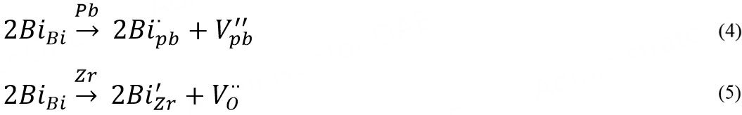
It can be seen that the point defect of  and
and  could be generated when Bi acts as a donor and acceptor dopant, respectively. Figure 4 shows the room temperature frequency dependency of dielectric properties for PZO-based films. As frequency increases, the dielectric properties of PZO-based films maintain stability over the frequency range of 1 kHz-1 MHz. Figure 4A shows that the dielectric constant enhances from ~250 for PZO films to ~325 for PBZ and PZB films, which may be related to an increased point defect contribution. In addition, Figure 4B illustrates that the dielectric losses of PZO-based films are around 0.1.

Figure 4. Frequency-dependent (A) dielectric constant and (B) dielectric loss for PZO-based films at room temperature. PZO: PbZrO3.
Figure 5A shows the room temperature P-E loops of PZO-based films at an applied electric field of

Figure 5. (A) The P-E loops of PZO-based films at 800 kV/cm, and corresponding (C) the polarization difference value of Δ P (Pmax - Pr). (B) The I-E loops of PZO-based films at 800 kV/cm, and corresponding (D) the switching field value of Δ E (EF - EA). PZO: PbZrO3.
Figure 6A shows the P-E loops of pure PZO films at different electric fields. As the electric field enhances, linear hysteresis loops gradually transform into double hysteresis loops causing Pmax to increase dramatically. With further improving the electric field, the P-E loops are unchanged and stay in a polarization saturation state. A detailed description of the division of regions into different states can be found in the following content. For PBZ and PZB films, the polarization saturation has a slight delay. Meanwhile, breakdown strength enhances compared to pure PZO films, as exhibited in Figure 6B and C. The leakage current is a crucial parameter for evaluating dielectric film's electric properties and conduction mechanisms[20-23]. Figure 6D illustrates the leakage current for PZO-based films as a function of the electric field. It can be seen that the curve of leakage current of pure PZO films can be divided into two parts: For low electric field, the leakage conductivity belongs to the bulk-limited Ohmic mechanism. The Fowler-Nordheim tunneling (FN) mechanism dominates at high electric field. A similar phenomenon also exists in PBZ and PZB films. Note that the transition field from bulk-limited to FN mechanism gradually reduces for pure PZO, PBZ, and PZB films, which may be related to different defect types in aliovalent doping PZO at A/B sites. Compared to the lead vacancy, the oxygen vacancy may easily contribute more leakage currier; hence, the transformation field of PZB from Ohmic into FN mechanism reduces compared to PBZ.

Figure 6. (A-C) The P-E loops of PBZ, PZB, and pure PZO films at different electric fields, respectively. (D) The leakage current functions of electric field for PZO-based films. (E) The recoverable energy density Wrec and (F) the energy efficiency η of PZO-based films at an applied electric field. PBZ: (Pb0.95Bi0.05)ZrO3; PZB: Pb(Zr0.95Bi0.05)O3; PZO: PbZrO3.
Figure 6E shows the recoverable energy density Wrec as a function of the electric field for PZO-based films. Similar to other literature[24], a corresponding curve can be divided into three regions as the electric field increases. For region I, PZO-based films possess a low Wrec value, which should belong to the AFE phase stage with a linear polarization curve. For region II, Wrec of PZO-based films both sharply enhance, which should correspond to AFE-FE co-existed phase stage. Note that the dashed and dot lines represent different terminal transition fields into region III, which means Bi dope PZO would delay the polarization enhancement. The Wrec only slightly enhances into region III, which should be attributed to the polarization saturation phenomenon at the high electric field[25,26]. The energy efficiency η as functions of electric field for PZO-based films is displayed in Figure 6F. Similarly, the curves of η also could be divided into three regions. As the electric field enhances, the η value gradually decreases and attains a relatively 50%-60% range. PBZ films achieve a maximum Wrec of 26.4 J/cm3 with a η of 56.2 %, which exceeds other reported pure AFE materials[27-29].
It is known that energy storage stability, including temperature and frequency[5,14,30], is an important parameter for evaluating the material applications, as shown in Figure 7. As temperature enhances, double hysteresis loop characteristics of PBZ films gradually transform into relaxor AFE, as shown in Figure 7A. Meanwhile, the Wrec gradually decreases and η value remains essentially unchanged (see Figure 7C), which should be related to the Curie temperature of PZO at about 230 °C, corresponding to the AFE-to-PE phase transition[8,31]. Figure 7B displayed frequency-dependent P-E loops of PBZ films at room temperature. As frequency enhances, polarization decreases and hysteresis loss also reduces. Therefore, the Wrec and η of PBZ films display good frequency stability, as shown in Figure 7D.

Figure 7. (A) Temperature-dependent P-E loops and corresponding (C) Wrec, η of PBZ films at 1 kHz. (B) Frequency-dependent P-E loops and corresponding (D) Wrec, η of PBZ films at room temperature. PBZ: (Pb0.95Bi0.05)ZrO3.
CONCLUSIONS
PZO, PBZ, and PZB films are prepared on Pt/Ti/SiO2/Si substrate via the sol-gel method. Crystallized PZO-based films with orthorhombic perovskite phases exhibit low roughness and good density. The dielectric constants of the Bi-doped PZO and pure PZO films are approximately 300, and these films possess good frequency stability at room temperature. Compared to pure PZO films, Δ E value increases and Δ P decrease for PBZ and PZB films hindering the effective energy storage. A/B-site doping in influencing the antiferroelectricity of PZO has a similar effect in only considering t value, and A-site doping would be better than B-site one in energy storage properties. PBZ films achieve a high Wrec of 26.4 J/cm3 with a η of 56.2 % under an applied electric field of 1278 kV/cm, accompanying a suitable temperature and frequency energy storage stabilities.
DECLARATIONS
Authors’ contributionsConceived the idea: Li D
Performed the experiments and data analysis: Li D, Guo Q, Cao M, Yao Z, Liu H, Hao H
Provided the technical support: Cao M, Yao Z, Liu H, Hao H
Wrote and reviewed the manuscript: Li D, Hao H
Availability of data and materialsNot applicable.
Financial support and sponsorshipThis work was supported by Major Program of the Natural Science Foundation of China (Grant No. 51790490), Foshan Xianhu Laboratory of the Advanced Energy Science and Technology Guangdong Laboratory (Grant No. XHT2020-011), Sanya Science and Education Innovation Park of Wuhan University of Technology (2020KF0017) and Guangdong Basic and Applied Basic Research Foundation (2022A1515010073).
Conflicts of interestAll authors declared that there are no conflicts of interest.
Ethical approval and consent to participateNot applicable.
Consent for publicationNot applicable.
Copyright© The Author(s) 2023.
REFERENCES
1. Yao Z, Song Z, Hao H, et al. Homogeneous/inhomogeneous-structured dielectrics and their energy-storage performances. Adv Mater 2017;29:1601727.
2. Yang L, Kong X, Li F, et al. Perovskite lead-free dielectrics for energy storage applications. Prog Mater Sci 2019;102:72-108.
3. Palneedi H, Peddigari M, Hwang G, Jeong D, Ryu J. High-performance dielectric ceramic films for energy storage capacitors: progress and outlook. Adv Funct Mater 2018;28:1803665.
4. Li D, Zeng X, Li Z, et al. Progress and perspectives in dielectric energy storage ceramics. J Adv Ceram 2021;10:675-703.
5. Pan H, Li F, Liu Y, et al. Ultrahigh-energy density lead-free dielectric films via polymorphic nanodomain design. Science 2019;365:578-82.
6. Qi H, Xie A, Tian A, Zuo R. Superior energy-storage capacitors with simultaneously giant energy density and efficiency using nanodomain engineered BiFeO3-BaTiO3-NaNbO3 lead-free bulk ferroelectrics. Adv Energy Mater 2020;10:1903338.
8. Hao X, Zhai J, Kong LB, Xu Z. A comprehensive review on the progress of lead zirconate-based antiferroelectric materials. Prog Mater Sci 2014;63:1-57.
9. Randall CA, Fan Z, Reaney I, Chen L, Trolier-mckinstry S. Antiferroelectrics: history, fundamentals, crystal chemistry, crystal structures, size effects, and applications. J Am Ceram Soc 2021;104:3775-810.
10. Zhao L, Liu Q, Gao J, Zhang S, Li JF. Lead-free antiferroelectric silver niobate tantalate with high energy storage performance. Adv Mater 2017;29:1701824.
11. Tagantsev AK, Vaideeswaran K, Vakhrushev SB, et al. The origin of antiferroelectricity in PbZrO3. Nat Commun 2013;4:2229.
12. Aramberri H, Cazorla C, Stengel M, Íñiguez J. On the possibility that PbZrO3 not be antiferroelectric. NPJ Comput Mater 2021;7:196.
13. Hao X, Zhai J, Yao X. Improved energy storage performance and fatigue endurance of Sr-doped PbZrO3 antiferroelectric thin films. J Am Ceram Soc 2009;92:1133-5.
14. Luo N, Han K, Zhuo F, et al. Design for high energy storage density and temperature-insensitive lead-free antiferroelectric ceramics. J Mater Chem C 2019;7:4999-5008.
15. Cai H, Yan S, Zhou M, et al. Significantly improved energy storage properties and cycling stability in La-doped PbZrO3 antiferroelectric thin films by chemical pressure tailoring. J Eur Ceram Soc 2019;39:4761-9.
16. Shimizu H, Guo H, Reyes-Lillo SE, Mizuno Y, Rabe KM, Randall CA. Lead-free antiferroelectric: xCaZrO3-(1-x)NaNbO3 system (0<x<0.10). Dalton Trans 2015;44:10763-72.
17. Guo H, Shimizu H, Mizuno Y, Randall CA. Strategy for stabilization of the antiferroelectric phase (Pbma) over the metastable ferroelectric phase (P21ma) to establish double loop hysteresis in lead-free (1-x)NaNbO3-xSrZrO3 solid solution. J Appl Phys 2015;117:214103.
18. Gao L, Guo H, Zhang S, Randall CA. A perovskite lead-free antiferroelectric xCaHfO3-(1-x) NaNbO3 with induced double hysteresis loops at room temperature. J Appl Phys 2016;120:204102.
19. Shannon RD. Revised effective ionic radii and systematic studies of interatomic distances in halides and chalcogenides. Acta Cryst A 1976;32:751-67.
20. Chiu F. A review on conduction mechanisms in dielectric films. Adv Mater Sci Eng 2014;2014:1-18.
21. Huang Y, Shu L, Zhang S, et al. Simultaneously achieved high-energy storage density and efficiency in (K,Na)NbO3-based lead-free ferroelectric films. J Am Ceram Soc 2021;104:4119-30.
22. Fan Q, Ma C, Ma C, Lu R, Cheng S, Liu M. Manipulating leakage behavior via thickness in epitaxial BaZr0.35Ti0.65O3 thin film capacitors. Appl Phys Lett 2020;116:192902.
23. Jiang X, Lv J, Chen Z, et al. Superior energy storage BaTiO3-based amorphous dielectric film with polymorphic hexagonal and cubic nanostructures. Chem Eng J 2022;431:133447.
24. Chen X, Cao F, Zhang H, et al. Dynamic hysteresis and scaling behavior of energy density in Pb0.99Nb0.02[(Zr0.60Sn0.40)0.95Ti0.05]O3 antiferroelectric bulk ceramics. J Am Ceram Soc 2012;95:1163-6.
25. Li D, Shen Z, Li Z, et al. Optimization of polarization behavior in (1-x)BSBNT-xNN ceramics for pulsed power capacitors. J Mater Chem C 2020;8:7650-7.
26. Ren Y, Cheng H, Ouyang J, et al. Bimodal polymorphic nanodomains in ferroelectric films for giant energy storage. Energy Storage Mater 2022;48:306-13.
27. Chen MJ, Ning XK, Wang SF, Fu GS. Significant enhancement of energy storage density and polarization in self-assembled PbZrO3: NiO nano-columnar composite films. Nanoscale 2019;11:1914-20.
28. Xu R, Wang M, Zhu Q, Xu Z, Feng Y, Wei X. Investigation on antiferroelectricity of Pb0.97La0.02(Hf1-xTix)O3 ceramics with low Ti content (0 ≤ x ≤ 0.1). J Am Ceram Soc 2022;105:7438-45.
29. Huang X, Zhang T, Wang W, Ge P, Tang X. Tailoring energy-storage performance in antiferroelectric PbHfO3 thin films. Mater Design 2021;204:109666.
30. Jiang X, Hao H, Zhang S, et al. Enhanced energy storage and fast discharge properties of BaTiO3 based ceramics modified by
Cite This Article
 , ... Hua Hao
How to Cite
Li, D.; Guo, Q.; Cao, M.; Yao, Z.; Liu, H.; Hao, H. The influence of A/B-sites doping on antiferroelectricity of PZO energy storage films. Microstructures 2023, 3, 2023007. http://dx.doi.org/10.20517/microstructures.2022.27
Download Citation
Export Citation File:
Type of Import
Tips on Downloading Citation
Citation Manager File Format
Type of Import
Direct Import: When the Direct Import option is selected (the default state), a dialogue box will give you the option to Save or Open the downloaded citation data. Choosing Open will either launch your citation manager or give you a choice of applications with which to use the metadata. The Save option saves the file locally for later use.
Indirect Import: When the Indirect Import option is selected, the metadata is displayed and may be copied and pasted as needed.
About This Article
Special Issue
Copyright


Comments
Comments must be written in English. Spam, offensive content, impersonation, and private information will not be permitted. If any comment is reported and identified as inappropriate content by OAE staff, the comment will be removed without notice. If you have any queries or need any help, please contact us at support@oaepublish.com.