


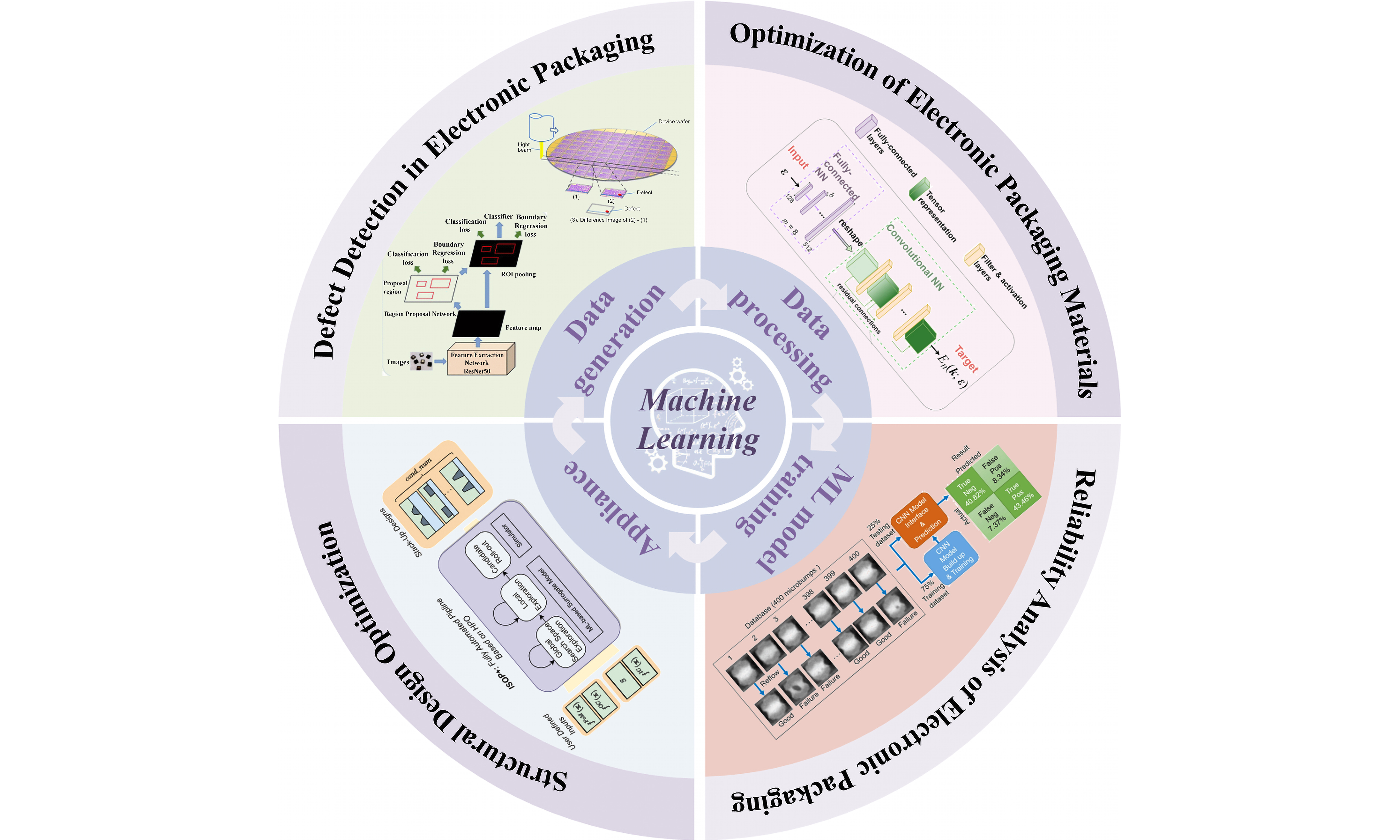
Machine learning-driven design and optimization of electronic packaging: applications and future developments
 0
0 Abstract
Machine learning (ML) provides robust solutions for electronic packaging, where growing complexity and miniaturization challenge traditional methods in design, defect detection, and performance optimization. This review systematically covers ML applications across key areas in electronic packaging, such as defect detection, material optimization, and reliability analysis, discussing key algorithms, data workflows, inherent challenges, and prospects. It aims to provide a clear roadmap and reference for effectively applying ML to innovate in this rapidly evolving field. However, addressing persistent challenges in data quality, model adaptability, and integration with established engineering practices remains vital for continued progress in this domain.
Keywords
INTRODUCTION
As the demands for performance, reliability, functionality, and size continue to increase in electronic products, the complexity of electronic packaging technology is also growing[1]. Electronic packaging not only provides physical protection but also needs to effectively manage heat and stress to ensure the product’s long-term reliability[2-4]. Traditional packaging design and analysis methods have shown apparent limitations when facing these complex requirements. These methods often rely on physical testing and manual design, which are time-consuming, costly, and cannot meet the modern electronic packaging industry’s need for efficiency and precision. Therefore, how to efficiently design, evaluate, and optimize packaging performance and reliability has become a critical issue that needs to be addressed in electronic packaging.
As an advanced artificial intelligence technology, machine learning (ML) has made significant breakthroughs in multiple fields[5,6]. ML can be divided into major categories: supervised, unsupervised, and deep learning. Standard ML models include fully connected neural networks, convolutional neural networks (CNNs), convolutional encoder-decoder networks, and generative adversarial networks (GANs)[7,8]. Data quality is fundamental to the application of ML[9,10]. The generation of vast amounts of experimental, sensor, and simulation data underscores the importance of data processing techniques. Traditional data analysis methods struggle to manage high-dimensional and complex datasets. At the same time, ML, through feature extraction (FE) and dimensionality reduction techniques, can extract valuable information from large-scale data, supporting modelling and optimization efforts. In electronic packaging, ML provides a new approach to address the challenges faced by traditional methods. It has been widely applied to automated defect detection and classification. By training on large volumes of labelled data, models can efficiently identify various defects in packaging, reducing the need for manual intervention. Meanwhile, unsupervised and deep learning can be used to analyze material performance data, uncover potential patterns, and optimize material selection and ratios, improving thermal management and mechanical strength in packaging. Moreover, the application of deep learning in reliability analysis has become increasingly important, as it can predict the long-term performance of packaging based on multi-dimensional data, enabling more precise lifecycle management and fault prediction and providing the basis for system optimization.
Although many studies have demonstrated the application of ML in specific aspects of electronic packaging, this review aims to provide a more comprehensive and critical integrated perspective. Our main contribution lies in systematically linking the fundamental levels, such as data generation and processing, with the practical deployment of various ML models in key challenge areas of electronic packaging, ranging from defect detection, material optimization, reliability analysis, and structural design. Furthermore, through a critical review of the mainstream challenges in each field and forward-looking planning of the future research trajectory, this paper strives to provide readers with not only a collection of current methods but also a valuable reference framework, aiming to help researchers select appropriate models more effectively and combine ML with traditional engineering practices. Thereby promoting the true innovation and development of electronic packaging technology.
DATA GENERATION AND PROCESSING
Generation of data
The data is continuously generated throughout the entire lifecycle of advanced packaging, including the design phase (interconnect materials and geometric data), manufacturing phase (processing/microstructure data), characterization phase (property data), deployment phase (performance data), and recycling phase (processing/cost data). Different stages of the lifecycle generate large volumes of data through parallel and automated experiments, which are then processed for analysis[11]. Since the Materials Genome Initiative (MGI) in 2011, an increasing amount of data has been generated in a high-throughput manner. High-throughput methods are widely used in computational and experimental materials science, leading to high-throughput computation, manufacturing, and characterization advancements. High-throughput experiments (HTE) are systematic experimental methods that can complete a large number of independent experiments in a short period of time to efficiently screen and optimize targets. The origins of HTE trace back to the early 20th century, including the discovery of the Haber-Bosch catalyst[12] and the Hanak multi-sample concept[13]. A landmark paper by Xiang et al. on HTE[14] garnered significant attention in the materials field, and HTE has since made notable advancements in areas such as dielectric materials[15], catalysis, and polymers. HTE typically combines materials science techniques to create libraries for synthesizing and characterizing materials, enabling the rapid determination of their structural, physical, and chemical properties. Because HTE can quickly establish relationships between composition, structure, and functional properties, it is an ideal experimental complement to computational simulations and modelling.
The advancements in HTE methods have been successfully demonstrated in various materials with significant technical value, proving that HTE can discover and deploy new materials at unprecedented speeds and low costs. First-principles calculations, particularly those based on more cost-effective approximation methods such as Kohn-Sham density functional theory (DFT), have facilitated the development of high-throughput techniques. High-throughput DFT (HT-DFT) calculations have become a powerful tool in new material discovery[16,17]. Furthermore, HTE can be reliably automated to predict the performance of large numbers of materials in high-throughput scenarios. High-throughput computation is widely used in material screening, discovery, and design. For example, Shen et al. used HT-DFT techniques for the computational and intelligent design of two-dimensional (2D) functional materials[18]. More studies exploring materials using high-throughput experimental methods are shown in Table 1[19-35].
Materials explored by high-throughput experimental techniques
To meet the quantitative demands of various materials for specific performance characteristics, a range of high-throughput characterization tools is required for fast and automated evaluation. Energy-dispersive spectroscopy (EDS) systems with silicon drift detectors (SDD) can fully meet the needs of high-throughput compositional measurements when combined with other functions, such as a thermionic field emitter. X-ray fluorescence (XRF) is also used for high-throughput compositional measurements[36,37]. Standard high-throughput characterization methods for material crystal structures include X-ray diffraction (XRD) and electron backscatter diffraction (EBSD). EBSD pattern collection times are 1 ms and offer sufficient spatial resolution to index the phases within a microstructure, enabling high-throughput characterization. Mechanical properties of materials can also now be characterized through high-throughput methods, such as micro-tensile testing to measure yield stress[38]. Zhao et al. used the diffusion multiple methods combined with nanoindentation to test the hardness properties of multi-component alloys, achieving results three orders of magnitude faster than traditional methods[39].
High-throughput experimental techniques can rapidly generate large amounts of experimental data, which is crucial for ML datasets. In addition, data quality is also vital. In-situ experiments provide high-quality, high-fidelity data for an in-depth understanding of the dynamic changes and damage evolution of electronic packaging during service. This data helps train reliable and trustworthy ML models. In-situ transmission electron microscopy (TEM) can characterize the evolution of microstructures in real time and is an effective tool for studying at the atomic scale[40]. The most advanced aberration-corrected TEM can achieve a spatial resolution of 0.5 Å[41,42]. At the same time, in-situ scanning electron microscopy (In-situ SEM) is often used to observe crack initiation and propagation on material surfaces[43]. In contrast, In-situ EBSD can effectively reveal microstructural evolution processes, such as changes in grain orientation and recrystallization under thermal and mechanical stress[44]. In-situ X-ray computed tomography (In-situ X-ray CT) demonstrates its unique tracking capabilities for the non-destructive observation of internal defects in packaging[45]. Furthermore, in-situ techniques can be combined with different physical fields, such as in-situ high-temperature experiments and in-situ tensile experiments[46]. Xu et al. recorded data related to intermetallic compound (IMC) growth and phase transition processes under Cu–Al bonding conditions through in-situ experiments, observing the dynamic evolution of the bonding interface[47]. Malkorra et al. characterized polymer core solder ball (PCSB) coatings using in-situ micro-pillar compression experiments to obtain the local mechanical properties of Cu and Ni-P layers[48]. Interconnection is an essential part of packaging, and researchers apply in-situ techniques to the interconnection process. Zeng et al. conducted an in-situ analysis of the solidification structure of lead-free interconnects; high-quality in-situ data guides manufacturing high-reliability lead-free micro-joints[49].
HTEs enable the generation and screening of large datasets, while in-situ experimental techniques achieve the exploration of high-quality data. Modern electronic packaging research is generating massive and diverse data at an unprecedented speed. This data, covering multi-dimensional information from composition and microstructure to macroscopic performance, forms the fundamental cornerstone for applying ML techniques to solve challenges in the packaging field.
Data preprocessing
The importance of datasets in ML is self-evident. High-quality datasets are the cornerstone of advancing research in electronic packaging science. However, raw data is often incomplete, inconsistent, lacking certain behaviors or trends, and may even contain errors. The logic used by ML models is learned from the data rather than encoded, so the data quality is crucial for achieving good model performance[50]. Therefore, further data processing is necessary to improve data quality and ensure the accuracy of ML model training. The primary data preprocessing methods include: data cleaning, feature selection (FS), FE, and normalization.
Data cleaning
Data cleaning detects or fixes corrupted, duplicate, incomplete, inaccurate, or noisy records in a dataset to improve its quality. Data cleaning provides high-quality datasets for ML, and at the same time, ML can also assist in the data cleaning process. These two processes are interrelated. Data cleaning is often a critical prerequisite for developing ML models. Many researchers have made significant advancements in creating innovative data-cleaning solutions. The most advanced data cleaning methods include Sample Clean[51], Active Clean[52], Holistic Data Cleaning[53], Alpha Clean[54], and CP Clean[55].
FS
A significant issue often arises when applying ML methods to large datasets: the curse of dimensionality (COD). This problem occurs when high-dimensional data becomes difficult to organize, classify, or analyze effectively in lower-dimensional spaces[56]. High-dimensional data significantly increases both the model’s computational complexity and storage requirements, spatial complexity. In such cases, dimensionality reduction becomes particularly important[57]. Not all features in the raw data are necessary; some may be irrelevant or redundant. FS becomes one of the most effective methods for dimensionality reduction, aiming to maximize relevance while minimizing redundancy. FS is selecting a subset of features from the original feature set based on specific criteria without transforming the features[58]. The subset selects relevant features from the dataset, thereby reducing the data processing scale, eliminating redundant and irrelevant features, improving learning accuracy, preventing model overfitting, and simplifying the learning outcome[59,60].
There are various classification standards for FS methods. The most common classification divides them into filter, wrapper, embedded, and hybrid methods[61]. Filter methods select features based on performance metrics without relying on learning algorithms to choose the feature subset. They are suitable for datasets with many features and can rank individual features or evaluate entire feature subsets[62]. Different types of tasks require distinct filter selections, which can be categorized into classification, regression, or clustering based on the task type[63]. Wrapper methods evaluate feature subsets based on the performance of a learning algorithm, treating the learning algorithm as a black-box evaluator. These methods typically have higher computational complexity but also offer higher accuracy[49]. Wrapper methods can theoretically be implemented using search strategies and learning algorithms, such as Naïve Bayes[64], linear support vector machines (SVM)[65], and extreme learning machines (ELMs)[66]. Embedded methods perform FS during training and integrate it as part of the algorithm’s core or extended functionality[67]. Hybrid methods combine filter and wrapper approaches: the filter method selects a candidate feature set from the original feature set, while the wrapper method refines this set through further evaluation. This approach takes full advantage of the strengths of both methods[68].
FE
Besides FS, which reduces the dimensionality of high-dimensional data, FE is also an effective data preprocessing method aimed at reducing redundant features and thus lowering the data’s dimensionality[69]. FE is typically used to construct a linear combination of continuous features αTx, which has strong discriminative power between classes[70]. Unlike FS, FE transforms the original features to generate more representative ones. The most commonly used FE method is principal component analysis (PCA), which performs a linear transformation of the data to minimize redundancy (measured by covariance) and maximize information (measured by variance)[71]. PCA involves an orthogonal transformation that converts samples of correlated variables into linearly uncorrelated features. The new features, called principal components, are fewer than or equal to the number of original variables[72].
Data normalization
Data normalization involves transforming features into a standard range to prevent more prominent numerical features from dominating smaller ones. The primary goal is to minimize the bias caused by features with larger numerical contributions when distinguishing between pattern classes. When the relative importance of features is unknown, all features are considered equally important in predicting the output class of unseen instances. This approach ensures that the features in the data have equal influence during the learning process. Data normalization significantly affects the quality of models in many ML studies aimed at building accurate predictive models. Algorithms such as k-nearest neighbors (k-NN)[73], artificial neural networks (ANNs)[74,75], and SVM[76] all involve the impact of data standardization and normalization on model performance. Researchers have proposed various normalization methods to process raw experimental data, including mean and standard deviation-based normalization[77-83], min-max normalization[84-86], decimal scaling normalization (DSN), median and median absolute deviation normalization (MMADN)[87], hyperbolic tangent (Tanh) normalization (TN)[88], and Sigmoid normalization[89].
ML ALGORITHMS
In ML, algorithms guide models through the data maze to find the optimal path to understand the essence of materials. The choice and optimization of algorithms directly affect the efficiency of model training and the accuracy of predictive results. The correct algorithm ensures the model learns effectively during training, avoids overfitting or underfitting, and guarantees good generalization. The revolution in deep learning has demonstrated the strong application potential of ML in materials science. There are various deep learning models, with the main ones being dense neural networks (DenseNets), CNNs, convolutional encoder-decoder, and GANs. Next, we will explain the key aspects of several different models when processing data, to help readers select the appropriate model for their data.
DenseNet
Highway Networks and deep residual networks (ResNet) have enabled neural networks to reach greater depths, with architectures easily exceeding 100 layers. However, as network depth increases, issues such as vanishing gradients and inefficient learning become more apparent. If shorter connections could be established between a CNN’s input and output layers, the network could train more deeply, precisely, and efficiently. Therefore, Huang et al. introduced a DenseNet, with the architecture shown in Figure 1[90]. It connects each layer to every other layer, except itself, through a forward-feedback mechanism. Unlike traditional convolutional networks with L layers, which have L connections, DenseNets feature L(L + 1)/2 direct connections. This design reduces the number of parameters, mitigates the vanishing gradient problem, and enhances feature propagation.
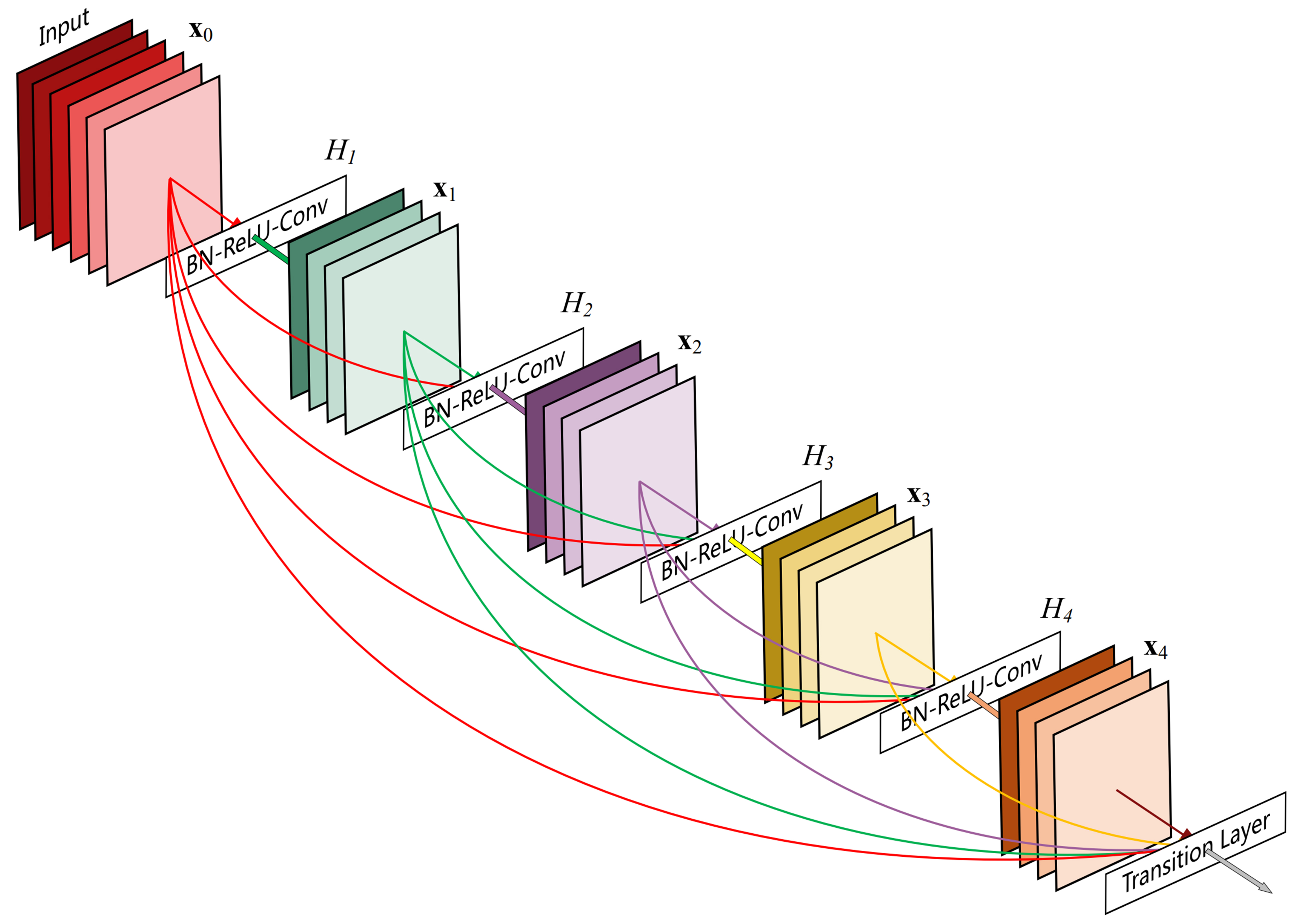
Figure 1. The DenseNet architecture: a 5-layer dense block with a growth rate of k = 4. Each layer takes all preceding feature maps as input[80]. DenseNet: Dense neural network.
Inspired by DenseNet, researchers have also proposed the DefectSegNet model for the automated identification of crystallographic defects and the TSRNet model to enhance the structural information in reconstruction outputs. Zhou et al. developed the scale-transferable detection network (STDN) for detecting multi-scale objects in images[91]. The network is integrated with DenseNet, creating a single-stage object detector equipped with an embedded super-resolution layer to explicitly explore the inter-scale consistency across multiple detection scales.
CNNs
DenseNets are the core of ANNs, but their input and output sizes are fixed. As mentioned earlier, DenseNets are typically used as part of a larger model and are rarely used alone. CNNs are one of the most representative neural networks in ML, with their development dating back to the 1980s[92]. The first milestone research in CNNs was LeNet-5, introduced by LeCun et al., initially used for document recognition[93]. The network architecture, as shown in Figure 2, consists of convolutional and pooling layers, followed by fully connected layers for classification tasks. The performance of this network outperformed any other network of its time.
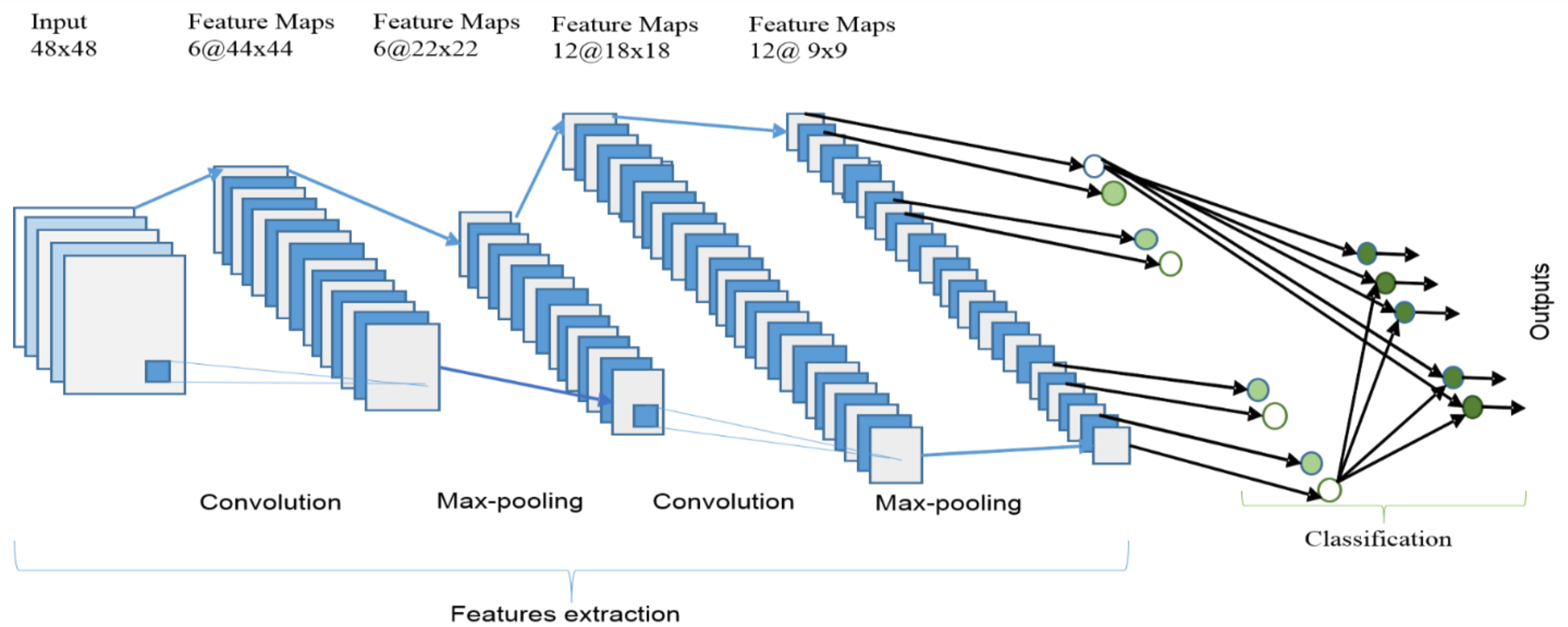
Figure 2. The overall architecture of the CNN includes an input layer, multiple alternating convolution and max-pooling layers, one fully connected layer, and one classification layer[94]. CNN: Convolutional neural network.
AlexNet, introduced in 2012, is a deep CNN consisting of 5 convolutional layers and 3 fully connected layers. The network includes 650,000 neurons and 60 million parameters, achieving top performance on the large-scale ImageNet ILSVRC-2012 dataset. Building on AlexNet, Simonyan and Zisserman introduced the deep convolutional networks VGG (Oxford Visual Geometry Group) -16 and VGG-19[95]. VGG-Net leverages its depth to learn more from the dataset, and its use of tiny convolutional filters significantly increased the network depth to 16 to 19 layers. As the network depth increases, the issue of vanishing gradients arises. To address this, He et al. designed the ResNet, which has a depth of up to 152 layers[96]. ResNet establishes shortcut connections by skipping one or more layers, allowing the network to access the output data directly, effectively mitigating the vanishing gradient problem.
CNNs include one-dimensional CNNs, 2D CNNs, and multi-dimensional neural networks. The evaluation of electronic packaging reliability often relies on microscope data, and 2D CNNs perform exceptionally well in processing microscopic images. Therefore, this section focuses on 2D CNNs. The core computation of a 2D CNN is the cross-correlation operation between the 2D input data and the 2D convolutional kernel. Farizhandi et al.[97] successfully processed image data of the amplitude decomposition process of Fe-Cr-Co alloys obtained through phase-field simulations using the pre-trained network EfficientNet, proposed by Tan and Le[98]. Kondo et al. also used CNNs to extract semantic features strongly associated with macroscopic properties automatically[99]. Kunwar et al. used CNNs to identify the presence of interface bubbles and IMCs during the hot-dip coating process of Cu strips[100]. Due to the small training dataset, data augmentation was performed before using CNN for recognition. This data preparation process is typically implemented using GANs in ML, which we will discuss in detail later.
Convolutional encoder-decoder
The convolutional encoder-decoder architecture is closely related to CNNs. Both use convolutional layers as the fundamental building blocks. A typical CNN structure consists of convolutional layers, followed by pooling layers, and ends with fully connected layers for classification output. The convolutional encoder-decoder is an extension built upon the CNN framework.
The convolutional encoder is based on the fully convolutional network (FCN) model[101]. In FCN, transposed convolutions or bilinear upsampling replace the traditional fully connected layers. In the convolutional encoder-decoder, the encoder is responsible for FE, while the attention module plays a key role in feature recalibration and enhancement. Attention mechanisms have shown outstanding performance in tasks such as image classification, object detection, semantic segmentation, and video understanding[102,103]. The “header” in the decoder connects the feature maps extracted by the encoder, generating rich feature maps and extracting contextual information. With its multi-level visual perception, the decoder can interpret hierarchical visual concepts and recover details[104,105]. Loss functions measure the difference between predictions and targets, guiding the training process. The model adjusts its parameters by minimizing the loss function to improve prediction accuracy. Different tasks require different loss functions, such as mean squared error (MSE), mean absolute error (MAE), and cross-entropy loss[106-114]. Typical formulations for these include:
MSE:
Where N is the number of samples, yi is the true value, and
MAE:
Cross-entropy loss (e.g., for binary classification):
where yi is the true label, typically 0 or 1, and
Typical encoder-decoder models include SegNet[115,116], U-Net[117-119], and the DeepLab series. SegNet consists of an encoder network, a decoder network, and a pixel-level classification layer (The architecture of SegNet is shown in Figure 3). The encoder network’s topology is consistent with the 13 convolutional layers of VGG16. The decoder network maps the low-resolution encoder feature maps to full-resolution feature maps for pixel-level classification. U-Net is one of the most important frameworks for semantic segmentation, widely used in image segmentation[120-123], image enhancement[124-126], and other fields. U-Net features a symmetric encoder-decoder structure, where the encoder progressively downsamples the input image to capture feature information while the decoder progressively upsamples to recover spatial resolution. Skip connections between corresponding features in the encoder and decoder preserve high resolution, which is a key feature of U-Net. Zhou et al. proposed the U-Net++ architecture, which differs from the previous architecture by redesigning the skip paths[118]. The encoder and decoder sub-networks are connected through a series of nested dense skip paths, reducing the semantic gap between their feature maps. This design achieved a 3.9 and 3.4-point improvement in mean IoU over U-Net and Wide U-Net, respectively. Chen et al. combined the responses of DCNN layers with conditional random fields (CRFs) to overcome the poor localization characteristics of deep networks, resulting in the DeepLab system[127]. This system outperforms previous methods, achieving more accurate localization of object boundaries. Chen
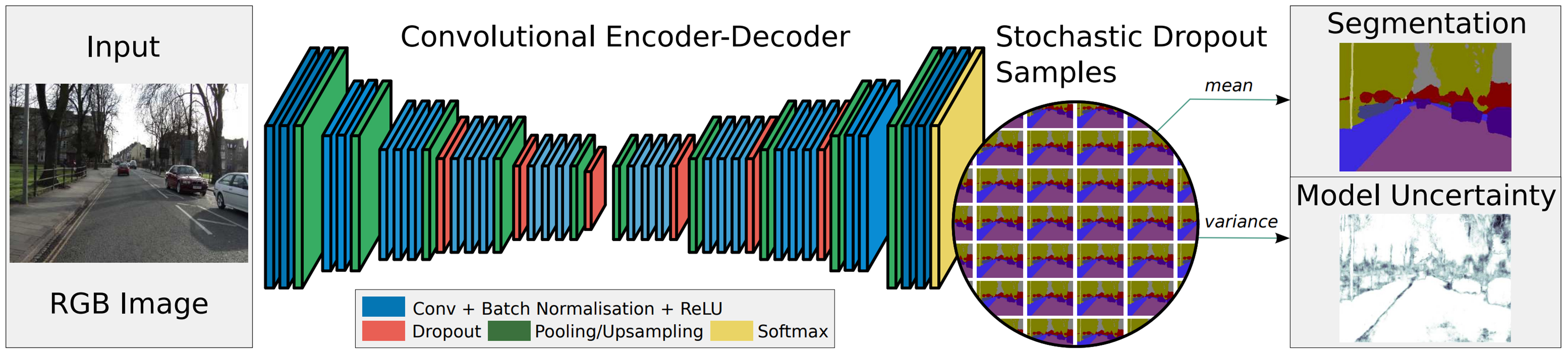
Figure 3. The architecture of SegNet[116].
The excellent performance of convolutional encoder-decoder models has led to their widespread application in materials science. Shrivastava et al. applied convolutional encoder-decoder models to predict peak stress clusters, particularly focusing on clusters’ size and other features within a heterogeneous linear elasticity framework[132]. Konstantinova et al. extracted features from images using convolutional layers, projected them into a lower-dimensional space, and then transposed convolutional layers to reconstruct clean images from this simplified representation[133]. Tsopanidis et al. employed the U-Net architecture to analyze the morphological features of fracture surfaces in MgAl2O4 samples, with experimental results demonstrating the model’s strong generalization ability and robustness[134].
GANs
A GAN consists of a generator and a discriminator. The generator aims to learn real data distribution and generate samples that closely resemble real data. In contrast, the discriminator aims to correctly determine whether the input data comes from real data or the generator. The generator and discriminator act as adversaries: the generator improves its ability to produce data closer to real data, while the discriminator enhances its ability to differentiate. This adversarial approach is based on the concept of Nash equilibrium from game theory[135]. The input to the generator G is a random variable z, which generates samples that follow a real data distribution. The discriminator D receives input data and labels it as 1 if it is from real data x, and 0 if it is from the output of the generator G(z).
Researchers have made improvements and theoretical extensions to the original GAN model to adapt to different analytical tasks. Goodfellow et al. first proposed GAN[135]. Similar to other neural networks, GAN also faces the issue of vanishing gradients. Arjovsky et al. replaced the traditional Jensen-Shannon divergence with the Wasserstein distance to obtain smoother gradients and achieve stable training[136]. Mao et al. proposed the least squares GAN (LSGAN), which replaces the cross-entropy loss function in traditional GANs with a least squares loss for the discriminator[137]. Berthelot et al. introduced a new balance-enhancing method to better balance the generator and discriminator training process[138]. They combined it with the Wasserstein distance loss to train autoencoder-based GANs. Furthermore, Conditional GANs (cGANs)[139,140] have been widely used as a general solution for various image-to-image translation tasks. Both cGAN and GAN are trained using paired images with one-way translation. Researchers introduced cycleGAN[141], DualGAN[142], and one-to-many cGAN to overcome these limitations[143].
GANs possess a unique game-theoretic concept, giving them significant advantages in data generation, data augmentation, and material design. Huang et al. designed a flexible Quantum GAN that generates high-dimensional feature images and utilizes quantum superposition to train multiple samples in parallel[144]. Kench et al. designed the SliceGAN architecture, which uses easily accessible 2D images to synthesize high-fidelity 3D data, achieving uniform information density[145]. Many researchers have leveraged GANs to assist in material design. Mao et al. used GANs to design complex materials with extreme properties in an unsupervised manner, without prior knowledge[146]. In GAN-based design, the discriminator network learns from the dataset to map the relationship between configurations and attributes, rapidly generating new configurations with extreme attributes. Dan et al. proposed a GAN-based generative ML model (MatGAN), which efficiently generates new hypothetical inorganic materials by training on materials from the ICSD database[147]. Narikawa et al. applied GAN-based deep convolutional GAN, cycle-consistent GAN, and super-resolution GAN techniques to generate, transform, and enhance the quality of microstructure images, reconstructing virtual microstructures that are nearly indistinguishable from real images[148].
ML IN ELECTRONICS PACKAGING
ML-based defect detection in electronic packaging
In the post-Moore era, electronic packaging dimensions are progressively shrinking[149], and consequently, solder joint sizes are diminishing, now reaching micrometre and even nanometer scales. This trend leads to size-dependent changes in microstructural features, such as grain size, thickness, and IMC. The formation of these IMCs is a primary contributor to solder joint failure, and an empirical formula typically governs their growth[150,151]:
X(t) represents the thickness of the IMC layer at time t, X0 is the thickness of the IMC at the initial moment, t is the time of the aging experiment, D is a constant depending on the activation energy and aging time, and n is a time constant.
Recognizing the influence of size on IMC growth, Zhu et al. refined the aforementioned empirical formula by introducing two size factors: B1 and B2[152]. These factors, which relate to the reaction rate and diffusion activation energy, respectively, account for the effect of solder joint dimensions on the growth of IMC thickness.
The IMC proportion is also affected by solder joint size. Magnien et al. studied the thickness and proportion of IMC in solder joints of different sizes[153]. The results indicate that the IMC thickness is directly proportional to the solder joint size, while the IMC proportion is inversely proportional to the solder joint size. As the solder joint size decreases, the diffusion of Cu from the boundary remains unchanged. This results in a higher concentration of dissolved copper in smaller solder joints, leading to a higher formation rate of the Cu3Sn phase. Huang et al. found that the growth rate of the IMC Cu6Sn5 is faster on fine-grained Cu than on coarse-grained Cu[154]. This is because fine grains provide more grain boundary channels, which promote rapid atomic diffusion. Therefore, solder joint size affects IMC morphology, which in turn affects IMC growth, ultimately leading to defects in the solder joint. The solder microstructure also changes with the decrease in size, especially for lead-free solders, where β-Sn is the main component. When the solder joint size decreases from the millimetre scale to the micrometre scale, the number of β-Sn grains that can be accommodated inside the joint gradually decreases. In extreme cases, the solder joint exhibits a single-crystal or near-single-crystal structure. β-Sn shows significant anisotropy in its diffusion, thermal expansion, mechanical, and electrical properties. This strong anisotropy significantly impacts the reliability of micro-solder joints during use[155-157]. The reduced solder joint size inevitably makes the impact of size-related local effects (such as current crowding, stress concentration, etc.) on the overall solder joint reliability more severe. Detecting solder joint defects becomes particularly important to ensure the overall reliability of solder joints. Manual visual inspection for defect detection is inefficient and lacks stability. Traditional image processing methods achieve high detection accuracy through image subtraction, but they are time-consuming. With the rise of deep learning-based defect detection techniques, many classical ML algorithms have been applied to defect detection in electronic packaging[158].
CNNs have been widely applied in image processing, object detection, and segmentation. The image preprocessing process is simplified by automatically extracting image features, leading to improved detection speed[159-162]. The essence of defect detection is identifying and locating defects or anomalies, which can be abstracted as an object detection task in deep learning. Therefore, object detection algorithms can be employed to perform defect detection tasks. Currently, object detection algorithms based on CNNs are most widely used in this field. They can be mainly divided into two categories: two-stage detectors represented by Region-based CNNs (such as Faster R-CNN), which are generally known for their high accuracy, and single-stage detectors represented by the “You Only Look Once (YOLO)” series, which are famous for their high-speed detection capabilities. Ren et al. integrated the region proposal network (RPN) with the Fast R-CNN object detection network, resulting in the new object detection system, Faster R-CNN[163]. The system is a unified object detection network consisting of two modules: the deep FCN (RPN) module for generating region proposals, and the Fast R-CNN detector that uses the proposed regions. Specifically, the RPN module indicates the areas on which the Fast R-CNN module should focus (The system architecture is shown in Figure 4A). Faster R-CNN enables a unified deep learning-based object detection system to operate at 5-17 frames per second (fps). The Faster R-CNN model has been widely applied to defect detection tasks[164-167]. Li et al. employed Faster R-CNN to detect five different types of printed circuit board (PCB) defects, achieving a mean average precision (mAP) of 60%, with approximately 90% accuracy in detecting Bridge and Empty type defects[168]. Ma et al. proposed an improved Faster R-CNN deep learning network[169]. The original Faster R-CNN performs multiple downsampling operations, making it challenging to achieve high-precision detection of minor defects on chip surfaces. Ma et al. replaced the original VGG16 backbone network with ResNet50, alleviating the gradient vanishing issue during model training and improving the accuracy of small defect FE. The improved system performs better in detecting and identifying chip surface defects, increasing the mAP of the original Faster R-CNN algorithm from 91.49% to 94.92% (The architecture of the improved system and the actual detection results are shown in Figure 4B-D). Hu et al. proposed a defect detection deep learning method more suitable for production environments[170], which is based on Faster R-CNN and incorporates the guided anchor (GA) introduced by Wang et al.[171]. In addition to using ResNet50 for FE, GARPN is employed to predict more accurate anchor points, and the residual units of ShuffleNetV2 replace the basic residual units to reduce the overall computational load of the network. To address the challenges of detecting small objects and objects with extreme aspect ratios on the surface of flexible printed circuit boards (FPC), Shen et al. proposed a new algorithm based on Faster R-CNN, called GA-Faster-RCNN[172]. The algorithm replaces the RPN network in the original Faster R-CNN with the GA module, leverages the feature pyramid network (FPN)[173] to enhance the FE capability for multi-scale defects, and substitutes ResNet-101 for VGG16 in the original Faster R-CNN. Overall, Faster R-CNN and its improved versions, as representatives of two-stage detectors, demonstrate high detection accuracy in electronic packaging defect detection tasks, especially when dealing with complex backgrounds and tiny defects, thanks to their RPN and fine-grained FE. However, this accuracy advantage often comes with relatively high computational complexity and slower detection speeds, which can be challenging in some production environments requiring real-time online inspection.
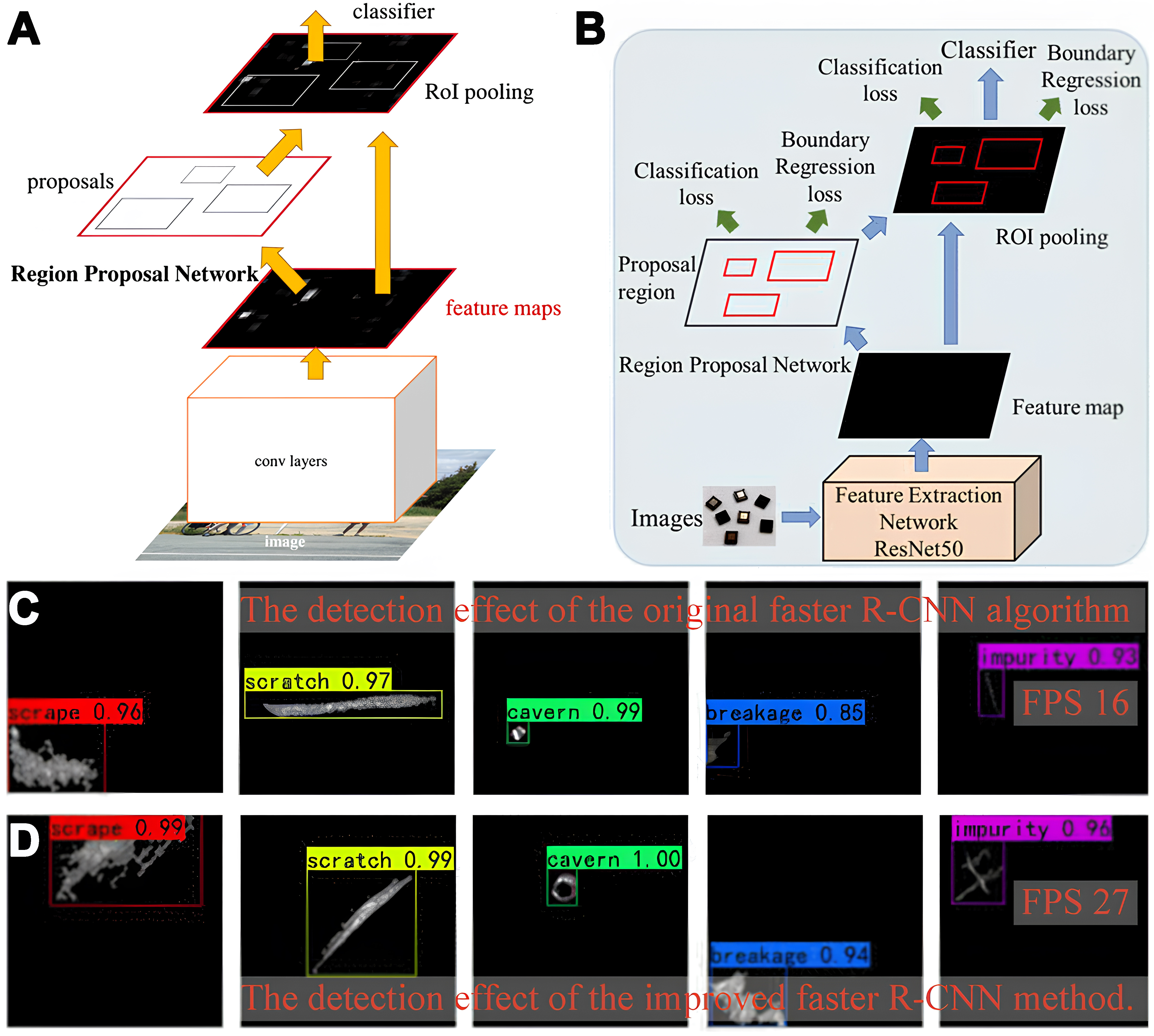
YOLO, a novel object detection method, was introduced in 2015. It offers good accuracy and fast computational speed by utilizing a single-stage network architecture to process images[174]. Unlike the two-stage detectors (such as Faster R-CNN) discussed earlier, YOLO integrates object localization and classification into a single network, significantly improving detection speed and making it a preferred choice for real-time applications. The first version of YOLO laid the foundation for real-time applications in machine vision systems[175]. Subsequently, researchers continuously improved YOLO, updating it from YOLOv1 to YOLOv10[176-182]. The YOLO series models, with their exceptional automatic detection capabilities, have been effectively applied in autonomous driving, particularly in scenarios that require efficient and accurate real-time detection systems[183-187]. YOLO demonstrates excellent real-time capability and accuracy performance. While early versions might have slightly lower accuracy than two-stage methods, subsequent versions have significantly improved accuracy through various optimizations while maintaining high speed. Mao et al.[188], based on the YOLOv7 model, utilized ConSinGAN[189] for data augmentation during the preprocessing stage and designed a dual in-line pin (DIP) defect detection system, achieving a detection accuracy of 95.5%. Cao et al. constructed a chip packaging surface defect dataset consisting of 2,919 images, the first dataset designed to detect defects across multiple chips simultaneously[190]. At the same time, the YOLOv7 model was optimized by incorporating the Carbon Border Adjustment Mechanism (CBAM) attention mechanism and the Receptive Field Block (RFB) module. New anchor boxes were designed for chip surface defect detection, and a novel post-processing method called CP-Cluster was introduced to replace the commonly used nonmaximum suppression (NMS). These improvements eliminated redundant structures in YOLO, enhancing detection accuracy and speed and reducing the number of parameters and computational workload. Lin et al. developed a system based on the YOLO algorithm for detecting capacitors assembled on PCBs[191]. In electronic packaging, the interconnection area is also a high-defect region. Many researchers have applied YOLO series models to solder joint defect detection, achieving high detection accuracy. Zou et al. created the Weld Defect Dataset (WDD) and trained a YOLOv3 object detection network on this dataset, achieving a detection accuracy of 75.5%[192]. Liao et al. adopted an improved deep learning algorithm, ConvNeXt-YOLOX, based on the YOLOX neural network[193]. This algorithm is primarily used for high-precision and high-speed detection of solder joint defects on surface mount technology (SMT) production line PCB assemblies (PCBA). Testing on the constructed dataset showed that the improved ConvNeXt-YOLOX model outperformed the original YOLOX model and the lightweight YOLOX-s model, achieving an average detection accuracy (mAP) of 97.21% (The architectures of the original YOLOX and ConvNeXt-YOLOX, along with their results in the test experiments, are shown in Figure 5).
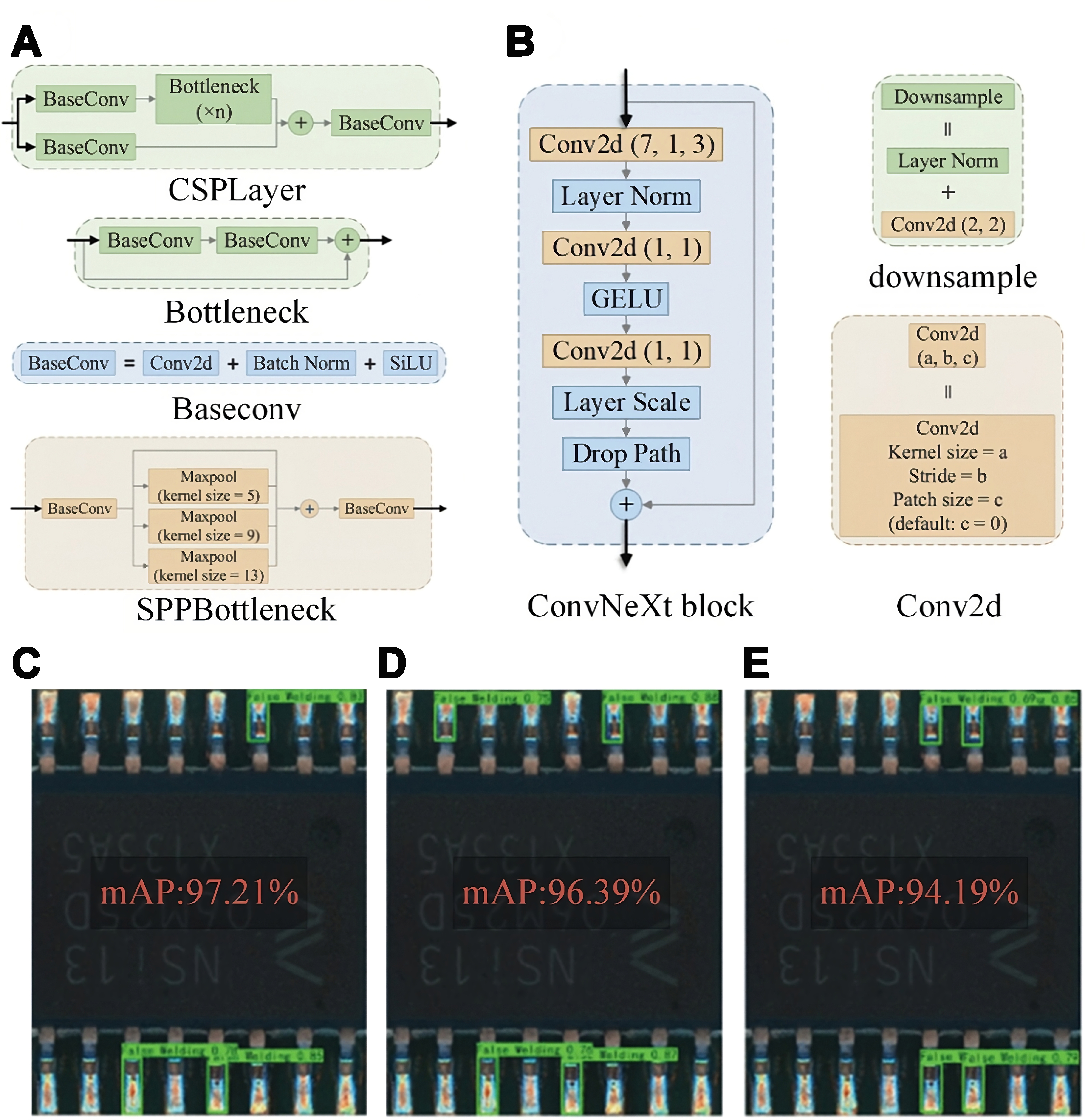
Figure 5. (A) Detailed structure of the original YOLOX model; (B) Detailed structure of ConvNeXt-YOLOX; (C) ConvNeXt-YOLOX results in PCBA solder joint defect detection; (D) YOLOX results in PCBA solder joint defect detection; (E) YOLOX-s results in PCBA solder joint defect detection[193]. PCBA: Printed circuit board assemblies.
The Faster R-CNN and YOLO frameworks are powerful tools for solving the defect detection problem. However, whether to pursue the typical high precision of a two-stage system or prioritize the pure speed of a single-stage system required for real-time detection is a matter that needs to be weighed. The scarcity of high-quality and labelled datasets remains a significant bottleneck. Meanwhile, the decreasing size of defects also brings difficulties in detection. Another major challenge is ensuring the model can operate stably in different environments. Considering these issues, future work is likely to promote more efficient data utilization methods, such as unsupervised learning and advanced data augmentation techniques, while also focusing on building network architectures that are both lightweight and intelligent enough to adapt to real factory environments.
ML-based optimization of electronic packaging materials
As electronic components continue to miniaturize, this trend leads to higher power density, which significantly increases the internal heat generation of the components. At the same time, the increased current density may reduce the functionality of electronic devices and adversely affect their long-term reliability. Therefore, selecting appropriate materials is crucial for enhancing the lifespan and reliability of electronic packaging[194]. ML methods offer scalability, automation, and cost-effectiveness when screening candidate materials with potential applications.
The combination of HT-DFT calculations and ML models facilitates precise atomic-level property estimation and the virtual screening of promising materials[195-197]. Tsymbalov et al. proposed a physics-based CNN model [Figure 6A and B] to promote autonomous deep learning of the electronic band structure of crystalline solids[198]. The model consists of a fully connected component and a CNN component. The strain components are processed through the fully connected layers and reshaped into a five-dimensional tensor. After several convolutional layers with residual connections to improve convergence, the network outputs the band structure, which matches the target band structure obtained from DFT calculations. Na et al. proposed a hybrid method that combines the graphical representation of materials and the crystal-level properties of the generalized gradient approximation (GGA) bandgap with a newly designed tuple graph neural network (TGNN) (the overall architecture of TGNN is shown in Figure 6C)[199]. This method leverages a given material’s crystal structure and GGA bandgap information to achieve accurate bandgap prediction. This research is essential for designing, developing, and applying semiconductor materials in electronic packaging. The traditional band gap calculation using the GW approximation and band gap estimation using the TGNN model are shown in Figure 6D. To validate the applicability of this approach, the researchers provided a dataset of G0W0 bandgaps for 45,835 materials predicted by TGNN. The input features for the GNN are the crystal structures of compounds and GGA bandgap data collected from the Materials Project dataset[200]. As shown in Figure 6E, the prediction error between the G0W0 bandgap and experimental bandgap is significantly smaller than the error between the calculated GGA bandgap and experimentally measured bandgap. Beyond these specific examples, ML is being broadly applied to tackle other critical aspects of semiconductor material optimization. Researchers are, for instance, using neural networks to bridge the gap between PBE calculations and experimental band gap measurements[201], employing ML to guide the design of novel nitrides based on first-principles data[202], and leveraging GANs for the inverse design and discovery of stable semiconductor materials[203]. Furthermore, ML frameworks are being developed to predict various physical potentials across diverse material classes with experimental-level accuracy[204]. These diverse applications underscore ML’s versatility in predicting known properties and actively guiding the search for and design of next-generation electronic materials.
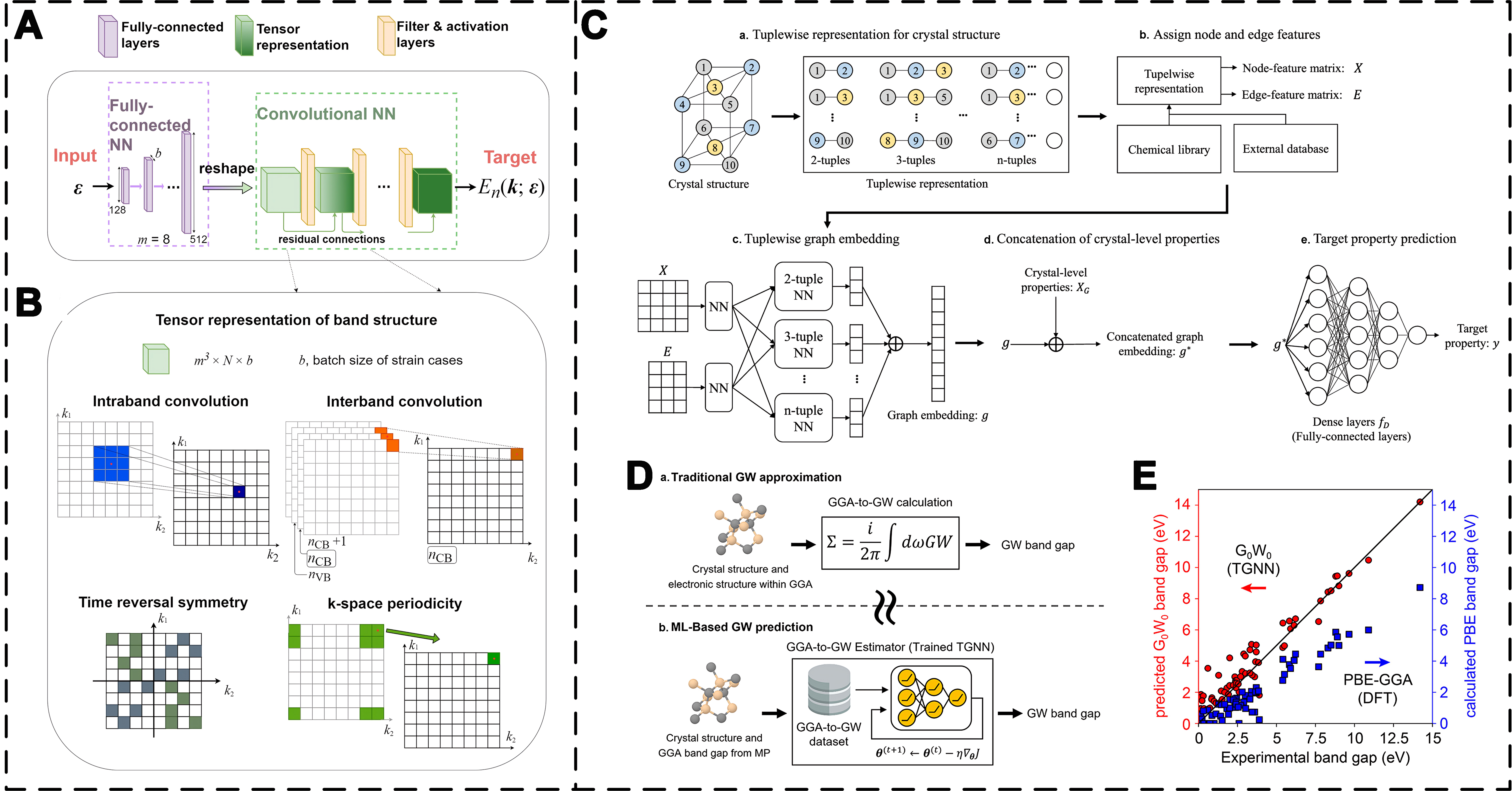
Figure 6. (A) CNN architecture for band structure prediction; (B) Tensor representation and physical insights incorporated into the CNN model; (C) Overall architecture of the TGNN and the crystal property prediction process based on TGNN; (D) a: Traditional band gap calculation using the GW approximation. b: Band gap estimation using the TGNN model; (E) Comparison between PBE-GGA (blue squares) and predicted G0W0 band gaps (red circles)[198,199]. CNN: Convolutional neural network; TGNN: tuple graph neural network; GW: GW approximation; PBE-GGA: Perdew-Burke-Ernzerhof generalized gradient approximation.
Epoxy resins are widely used in electronic encapsulation due to their excellent adhesive properties, thermal stability, electrical insulation, and mechanical strength. Pruksawan et al. addressed this issue by combining laboratory experimental design, an active learning process, and Bayesian optimization to predict and optimize adhesive materials[205]. The approach was implemented in two phases: in the first phase, an accurate ML model was developed for active learning; in the second phase, experimental conditions were improved to enhance Bayesian optimization. This two-stage data-driven approach successfully identified adhesive materials with exceptionally high adhesive strength from a minimal dataset. Jin et al. proposed an optimization method for multi-component epoxy resin systems based on molecular dynamics (MD) and ML[206]. The method uses MD simulations to generate a training dataset, then applies ML to determine the optimal component ratio, and finally validates the results experimentally. The optimized composition ratio of diglycidyl ether of bisphenol A / tetraglycidyl diaminodiphenyl methane / diaminodiphenyl sulfone / polyethersulfone was 10.5/51.23/29.63/8.64. Compared to the designed average values, the glass transition temperature (Tg) increased by 17.3%, the modulus of elasticity (E) increased by 15%, the ultimate tensile strength (UTS) increased by 32.7%, and the elongation at break (δ) increased by 85.5%. These two studies showcase different ML strategies for polymer optimization: Pruksawan et al. employ an active learning approach to minimize costly experiments, while Jin et al. leverage computationally intensive MD simulations to generate rich datasets for ML-driven multi-objective optimization, demonstrating the adaptability of ML to both data-scarce and data-rich scenarios[205,206].
ML is rapidly becoming an indispensable tool in electronic packaging. It accelerates the prediction of the core properties of semiconductors to help design complex mixtures such as epoxy resin. However, some significant obstacles remain before ML can thoroughly guide material design. One major challenge is bridging the scale gap - reliably converting atomic simulation or experimental data into predictions of fundamental macroscopic properties, achieving reverse design, and creating entirely new materials on demand. Ultimately, the close integration of ML and material design will likely determine the pace of future innovation in advanced packaging materials.
ML-based reliability analysis of electronic packaging
The reliability of electronic packaging directly determines the overall performance and lifespan of electronic products. As electronic devices continue to become smaller and more integrated, the reliability of electronic packaging faces increasingly stringent challenges. Reliability analysis helps identify potential failure modes, preventing device malfunctions or performance degradation caused by packaging failures. Reliability analysis of electronic packaging has always been based on powerful experimental techniques [such as EBSD, digital image correlation (DIC)] and physics-based models [such as crystal plasticity finite element (CPFE)]. Although these mature methods provide deep physical insights, they face challenges regarding computational cost and large and complex data analysis. This presents an opportunity for ML to serve as a complementary tool by accelerating simulations, interpreting experimental data, and creating novel predictive models, which are the focus of this section.
Non-uniform heat flux and temperature distribution often compromise the reliability of advanced packaging and heterogeneous integration. Physics-based models are widely used to predict package-level reliability. MD and first-principles calculations are indispensable simulation tools for analysis at the microscopic and atomic scales. First-principles calculations are algorithms that directly solve the Schrödinger equation based on the principles of quantum mechanics[207]. These calculations are founded on the interactions between atomic nuclei and electrons and their fundamental laws of motion, with certain approximations applied. Zhang et al. employed first-principles calculations to analyze Ni-Sn-based IMCs used in high-power device packaging[208]. This work guides the microstructural design and process development of all IMC solder joints in the Ni-Sn system. Based on first-principles calculations, Fu et al. analyzed the formation difficulty of Cu6Sn5 and Cu3Sn from a microscopic perspective[209]. They also investigated the interfacial failure mechanism from an energetic standpoint. Increasing chip integration density has led to a continuous reduction in package dimensions. This makes interfacial observation extremely difficult, for instance, with barrier layers in through-silicon vias (TSVs) that are only 100 nanometers thick or thinner. MD, a vital simulation method for addressing issues at the atomic and molecular level, is highly effective for analyzing the dynamic properties of nanoscale materials[210]. Therefore, it is also well-suited for analysing and predicting materials in such small-scale packages. Using MD simulations, Gao et al. analyzed different Cu/Ta interface models and performed tensile simulations[211]. Their findings showed that the critical strain energy release rates for rough and tilted interfaces were higher than those of a perfect interface. They also found that interfacial voids significantly reduced the energy release rate. Ji et al. utilized MD to investigate the influence of IMCs on the Cu/Si interface[212]. They evaluated the interfacial fracture performance based on stress, strain, and critical strain energy release rate, ultimately finding that an IMC layer of a specific thickness can improve the fracture properties. The anti-corrosion performance of two organic encapsulation materials, polydimethylsiloxane (PDMS) and hexamethyldisilane (HMDSO), on copper surfaces was investigated by Zhang et al. using MD[213]. This research provides valuable insights into the corrosion-related reliability of electronic packages.
Physics-based models have long been indispensable tools in electronic packaging reliability analysis. They provide a fundamental understanding of the physics of failure and enable detailed, multi-scale observations. However, their significant computational cost, both in time and resources, severely limits their application for macro-scale system analysis, large-scale parameter optimization, and real-time health monitoring. Researchers increasingly turn to data-driven ML methods to overcome these shortcomings and establish rapid mappings from experimental or simulation data to system performance.
ML methods can achieve high accuracy in forecasting reliability issues caused by junction temperature variations[214-217]. Researchers are increasingly focusing on using ML methods to predict and optimize the thermal reliability of electronic packaging systems. A junction temperature prediction method based on the back propagation (BP) neural network is proposed, with prediction accuracy superior to traditional polynomial fitting methods[218]. Other researchers have combined BP neural networks, interpolation methods, and Kalman filtering for junction temperature prediction. Although the accuracy has been improved, the high computational complexity may limit its practical applicability[219]. Wang et al. proposed an enhanced multi-feature electro-chemo-thermal coupling modelling method, combined with an improved decoupled modified bias extended Kalman filter method, for iterative state of charge (SOC) prediction, achieving more robust prediction results[220]. They also proposed an improved multi-head bidirectional long short-term memory (LSTM) temporal convolutional model for lithium-ion battery SOC estimation[221]. In addition, they established a back propagation neural network - square-root cubature kalman filter (BPNN-SRCKF) estimation model based on fusion dual-factor parameter identification to achieve accurate and reliable online SOC estimation[222]. Gharaibeh et al. optimized an ANN deep learning model by adjusting the number of hidden layers and the number of neurons in each layer to predict the temperature distribution of four chips in a multi-chip module (MCM) under both uniform and non-uniform heat flux[223]. In the case of uniform heat flux, the neural network has one hidden layer with 10 neurons, while in the case of non-uniform heat flux, the network has three hidden layers, each containing 4 neurons. In both scenarios, the model’s prediction R2 value was 0.99. This model successfully predicted the temperature distribution under different heat flux conditions, aiding in the real-time evaluation of the thermal reliability of MCMs. Djedidi et al. conducted a study on the reliability of systems on chip (SoC) in applications, using a nonlinear auto-regressive (NAR) neural network to model the temperature drift trend[224]. When the estimated error of the actual drift exceeds a predefined threshold, the model is updated, enabling real-time prediction of the SoC’s remaining useful life (RUL). ELM is a ML model known for its strong fitting and classification capabilities, and it offers faster learning speeds than traditional feedforward neural networks[225]. Liu et al. proposed an ICS-ELM model based on an improved Cuckoo Search optimization method for ELM[226]. This model takes saturation voltage drop, collector current, and aging cycle count as inputs and predicts junction temperature as the output, establishing a multi-input, single-output insulated-gate bipolar transistor (IGBT) junction temperature prediction model with high accuracy. Majd et al. collected temperature, shear stress, and differential stress time series data from multiple electronic packages using piezoresistive silicon-based strain sensors in a thermal shock chamber and then analyzed the data using various neural network models[227].
In electronic packaging, solder joints provide electrical interconnection and mechanical support for electronic devices. Therefore, evaluating the reliability and predicting the lifetime of solder joints has always been a significant challenge for researchers[228-230]. While traditional statistical models such as Weibull regression and the Cox proportional hazards model (Cox-PHM) have long been employed for reliability analysis due to their simplicity[231-235], they often struggle to capture the complex, multi-factor interactions inherent in modern packaging failures, thus paving the way for ML approaches.
The reliability of solder joints is influenced by multiple factors, including thermal variations, the mechanical properties of the solder joint itself, electromigration during service, and the formation of IMCs[236-239]. ML methods can comprehensively capture the interactions between these competing factors, enabling high-fidelity predictions of solder joint lifetime while accelerating the development of predictive models for reliability assessment. Samavatian et al. proposed a correlation-driven neural network (CDNN) model that captures correlations between candidate features and accurately predicts lifetime based on material properties, device configuration, and thermal cycling, with a root mean square error of just 5.71%[240]. The model also analyzed the effects of solder material and thickness on joint failure evolution and estimated the optimal solder layer thickness balancing creep and fatigue damage. The reliability of 3D integrated circuits (ICs) faces more significant challenges. Hsu et al. used AI deep learning based on CNNs for non-destructive analysis of typical 3D IC chips with solder micro-bumps using 3D X-ray tomography images (Figure 7 shows the test samples, the training/testing procedure, and performance of the CNN model)[241]. Training the model with a collected image database can quickly predict solder joint interconnection failures based on non-destructive 3D X-ray tomography images with an accuracy of up to 89.9%. The study identified key features determining the “good” or “faulty” conditions of reflowed micro-bumps, such as the percentage of area loss in the middle cross-section. Yuan et al. combined sequential ANNs with finite element modelling to generate datasets based on finite element analysis (FEA)[242]. They trained the datasets using recurrent neural networks (RNN) and LSTM architectures to evaluate the thermal cycling performance of solder joints in glass wafer-level chip-scale packaging (G-WLCSP). Reihanisaransari et al. considered the effects of BGA chip position, PCB thickness, solder alloy composition, and solder ball volume on solder joint reliability[243]. They obtained training data for a neural network model through 480 finite element simulations and 20 experimental tests. Using the trained neural network model, they successfully predicted the solder joint reliability with an accuracy of 97.55%. The above content summarizes different ML strategies for solder joint reliability: some use neural networks to learn directly from experimental or simulated data [such as CDNN or NN+finite element method (FEM)], while others use CNNS to analyze non-destructive imaging data (such as 3D X-rays). They can handle high-dimensional inputs and discover hidden correlations that traditional models might overlook. However, the breadth and high quality of the training data (whether from FEM or experiments) remain one of the challenges to be overcome, and it is also necessary to ensure that the ML model captures the underlying mechanisms of faults rather than just statistical correlations. Effective integration of multimodal data (such as thermal, mechanical, and imaging) remains an important goal.
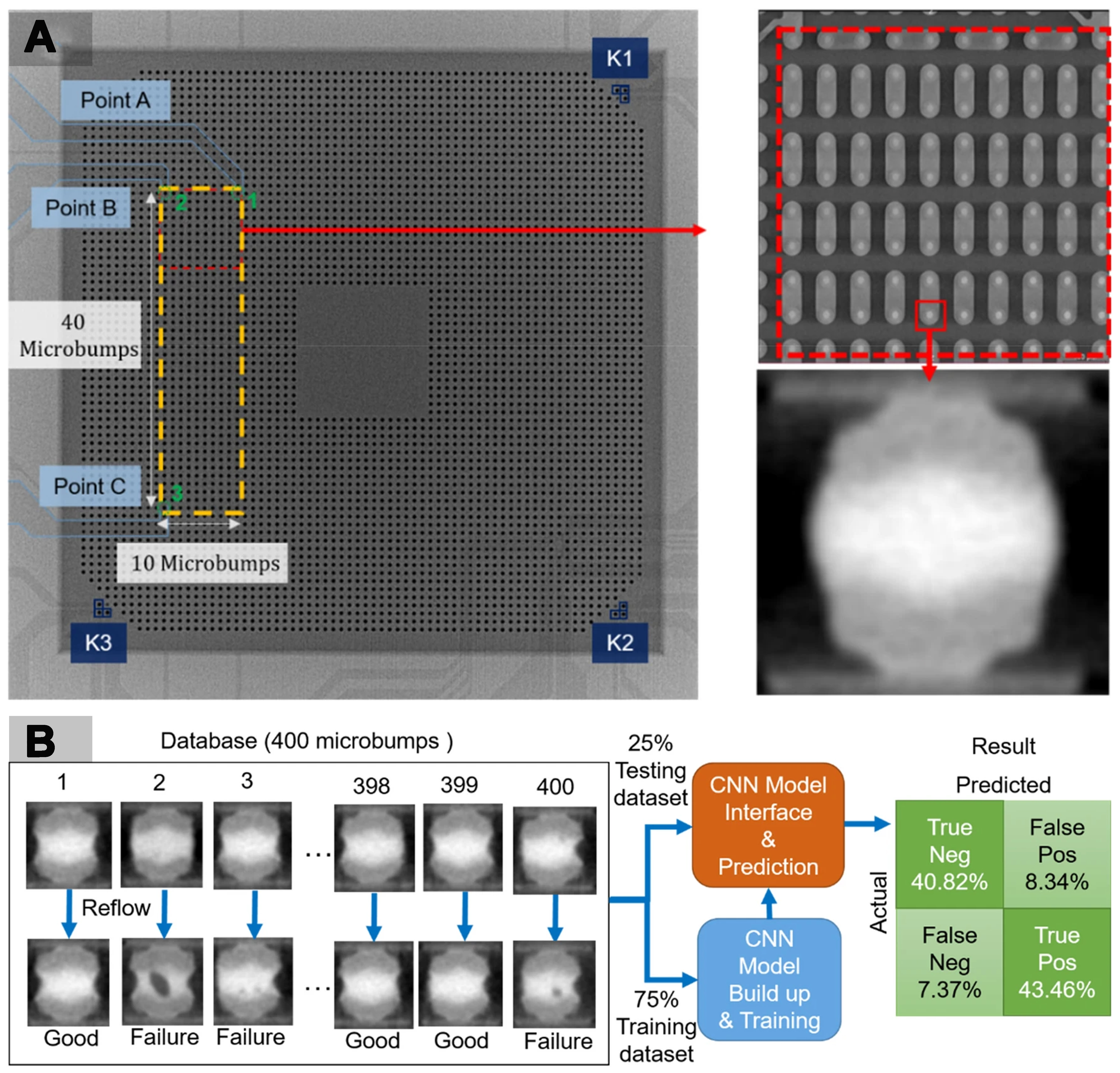
Figure 7. (A) Overall image of the test sample; (B) CNN model training/testing procedure and performance[241]. CNN: Convolutional neural network.
In conclusion, ML is transforming the reliability analysis of electronic packaging, moving beyond traditional statistics and towards predictive, data-driven approaches. However, the path forward requires overcoming key obstacles: generating high-fidelity life cycle data, integrating physical knowledge into ML, and developing interpretable models suitable for the working environment. The “Digital Twins” concept combines real-time data, physics-based simulation, and ML and may represent the future direction of comprehensive reliability management in this field.
ML-based structural design optimization for electronic packaging
A well-designed structure significantly influences electronic packaging systems’ reliability, thermal management, electrical performance, and mechanical strength[244-246]. Researchers have extensively studied micro-bump layout design, packaging design under plastic encapsulation, flip-chip interconnection design, and high-power multi-chip structure design in electronic packaging[247-249]. However, due to limitations in experimental costs and computational capacity, a systematic approach for packaging structure optimization has yet to be established, hindering chip designers from effectively determining the optimal design parameters for their products.
Flip-chip packaging technology is widely used in the electronics packaging industry, eliminating the need for wire connections and achieving the shortest connection paths. Compared to wire bonding (WB) and tape automated bonding (TAB), it offers higher packaging density, smaller package size, superior electrical and thermal properties, and lighter weight[250-253]. However, this technology still faces specific challenges. As mentioned earlier, selecting the appropriate materials is crucial for improving packaging reliability, and additionally, the design of the interconnection structure layout plays a significant role. Wu et al. developed a FEA model, varying chip thickness, width, and PCB board thickness to obtain the corresponding maximum first principal stress, which was used as training data for ML models[254]. The models were trained using ordinary least squares linear regression, lasso regression, ridge regression, Poisson regression, bagging regression, support vector regression (SVR), KNN, and random forest (RF) algorithms for prediction. The comparison revealed that the RF algorithm provided the best stress prediction capability for chip packaging integration design. However, FEA-based ML methods typically rely on temporary data generation procedures, which are less efficient and struggle to handle increasing chip design parameters. Chu et al. adopted an efficient statistical sampling method for generating training data using computer models[255]: the Latin hypercube sampling (LHS) scheme[256]. This method was used to create the initial dataset for training the ML model, and an ANN model was developed for ERR prediction, applied to reliability prediction, and design optimization of ultra-low-k chip packaging. To capture the nonlinear data patterns and input-output electrical relationships of analogue circuits, Lai et al. employed ML techniques to improve the packaging and testing processes of analogue ICs[257]. This approach enabled rapid prediction of resistance (R), inductance (L), and capacitance (C) values, thereby providing a basis for improvements in structural design.
High-performance PCB designs have evolved to 12 to 20 layers. Each layer contains various signals sensitive to the stacked physical design, which significantly increases the complexity of the stacking design[258]. Long et al. proposed a method that uses ML to rapidly generate models and analyze electronic packaging structures’ mechanical behavior[259]. Chae et al. proposed a reverse stacking optimization method for advanced packaging design (ISOP+), which utilizes an automatic search algorithm and a ML surrogate model to generate stacking designs optimized for performance requirements directly[260]. Experimental results indicate that the ISOP+ framework reduces the design cycle from several hours to just a few minutes and significantly outperforms other baseline optimization methods and manual designs.
ML facilitates the design of three-dimensional electronic packaging structures, effectively addressing the growing complexity of packages. The increasing intricacy of 3D electronic packaging poses significant inspection challenges. While physical cross-sectional analysis is destructive, 3D X-ray microscopy (XRM) offers a non-destructive alternative, generating comprehensive volumetric data via full-angle tomography for reconstructing detailed internal architectures[261]. Figure 8A shows the workflow. Given the substantial spatial information involved, ML techniques are crucial for efficiently processing these datasets and facilitating 3D reconstruction and defect identification. Deep learning high-resolution reconstruction (DLHRR) methods[262] can significantly accelerate 3D X-ray scans for complex packages and overcome significant field-of-view limitations[263].
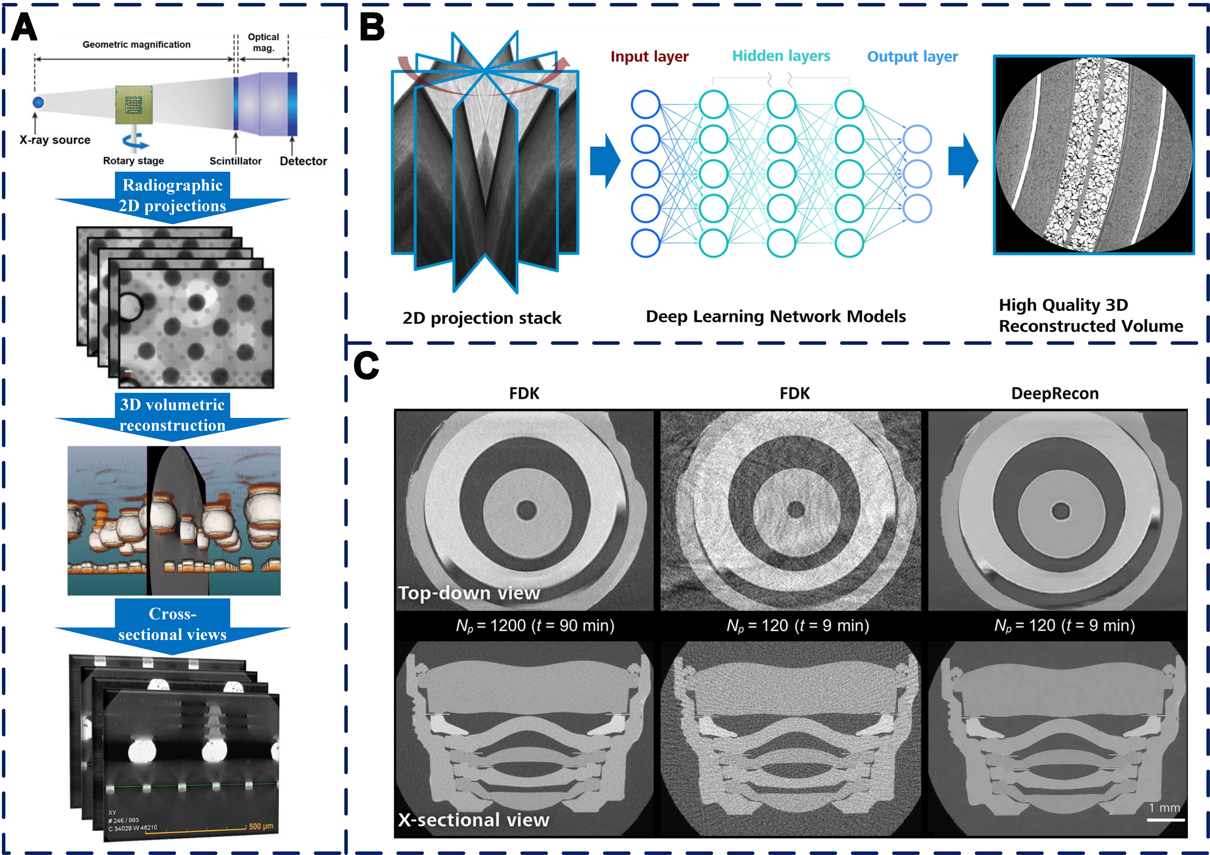
Figure 8. (A) Workflow for 3D XRM measurement; (B) Deep learning network model: reconstruct a high-quality 3D XRM volume dataset with low noise and minimal artefacts through a small amount of X-ray projection and/or exposure time; (C) XRM data for lens components of smartphone cameras: FDK and DeepRecon comparison[264]. XRM: X-ray microscopy; FDK: Feldkamp-Davis-Kress.
ML offers a novel approach to the design of packaging structures and integrates with 3D X-ray technology to analyze these structures, thereby enhancing analytical efficiency, accelerating development processes, and assisting in identifying and rectifying potential defects in packaging structures within practical applications. By establishing a CNN bridging 2D projection and 3D reconstruction (as depicted in Figure 8B), the network can be trained to disregard noise within the data and emphasize small-scale features. This approach mitigates noise and artefacts in the reconstruction outcomes while retaining edge characteristics and fine surface details[264]. Carl Zeiss X-ray Microscopy (XRM) Inc. has recently incorporated a deep learning-based CT reconstruction workflow, called DeepRecon, into its 3D XRM workflow. Compared with the conventional standard algorithm, this approach enhances image quality by up to four times [Figure 8C] and, in specific scenarios, increases throughput by as much as tenfold[265,266]. Certain materials, such as metal foam, can only be subjected to 3D scanning with a minimal field of view, thereby impeding the reconstruction process. Zhang et al. used optimized neuroimplicit X-ray imaging (ONIX)[267]. This DL algorithm can retrieve continuous 3D object representations from limited views, to enhance the volumetric information and capabilities of 3D X-ray stereoscopic imaging.
The application of ML in designing and optimising electronic packaging structures is gaining momentum. ML offers powerful new approaches, from optimizing PCB stacking to enhancing 3D structure analysis through X-rays. However, the main difficulties are seamlessly integrating ML into complex CAD and FEA workflows and embedding key physics-based constraints into data-driven models. Furthermore, generating sufficient high-quality data and ensuring the interpretability of ML-driven designs are also persistent issues. The future direction may involve more complex generative design methods (using GANs or reinforcement learning), multi-objective optimization frameworks that balance thermal, mechanical, and electrical performance, and closer integration between ML-driven design and advanced destructive analysis.
CONCLUSIONS AND OUTLOOK
This review has provided a systematic and structured overview of ML in electronic packaging, from data generation to key areas such as defect detection, material optimization, reliability analysis, and structural optimization. It has been underscored that while advanced algorithms can handle complex data, the quality of data. Remains interdependent with algorithmic sophistication for successful outcomes. Plays a crucial role in the performance of ML models, even as some algorithms are designed to handle high-dimensional, complex data, indeed, data quality and algorithmic sophistication are interdependent factors contributing to successful outcomes. By detailing current innovations and the underlying models, this work aims to offer researchers and engineers a valuable reference framework and a more precise roadmap for leveraging ML in this evolving field.
Despite the significant progress in applying ML, this review has also systematically analyzed persistent challenges: unstable data quality, incomplete datasets, limited model generalization, and operability in real-world applications. Consequently, building upon this analysis, future research should strategically focus on enhancing data ecosystems, fostering innovation in model efficiency and generalization, and promoting the synergistic integration of ML with complementary technologies such as Internet of Things (IoT) and big data. This holistic approach is anticipated to unlock further innovative potential for design and optimization in packaging.
In conclusion, as this review has systematically detailed and framed, ML has great potential in electronic packaging. Future research will continue to drive innovation and progress in this field, improving efficiency, accuracy, and reliability in electronic packaging and ensuring better performance for electronic products.
DECLARATIONS
Authors’ contributions
Writing-original draft, data curation: Chen, X.
Validation, resources, data curation: He, S.
Project administration: Paik, K. W.
Writing-original draft, funding acquisition: Wong, Y. H.
Writing - review and editing, supervision: Zhang, S.
Availability of data and materials
Not applicable.
Financial support and sponsorship
The authors acknowledge the financial support from the National Natural Science Foundation of China (U21A20128), Heilongjiang Provincial Natural Science Foundation of China (No. YQ2022E024), and the open research fund of Songshan Lake Materials Laboratory (No. 2023SLABFN33).
Conflicts of interest
All authors declared that there are no conflicts of interest.
Ethical approval and consent to participate
Not applicable.
Consent for publication
Not applicable.
Copyright
© The Author(s) 2025.
REFERENCES
1. Lau, J. H. Recent advances and trends in advanced packaging. IEEE. Trans. Compon. Packag. Manufact. Technol. 2022, 12, 228-52.
2. Tong, X. C. Electronic packaging materials and their functions in thermal managements. advanced materials for thermal management of electronic packaging. New York: Springer; 2011. pp. 131-67.
3. Tang, S.; Chen, J.; Hu, Y. B.; et al. Brief overview of the impact of thermal stress on the reliability of through silicon via: analysis, characterization, and enhancement. Mater. Sci. Semicond. Process. 2024, 183, 108745.
4. Zhang, S.; Qiu, Q.; Ding, T.; et al. Investigation of isothermal aged Sn-3Ag-0.5Cu/Sn58Bi-Co hybrid solder joints on ENIG and ENEPIG substrate with various mechanical performances. Mater. Today. Commun. 2024, 39, 108609.
5. Hu, W.; Jing, E.; Qiu, H.; Sun, Z. Discovering polyimides and their composites with targeted mechanical properties through explainable machine learning. J. Mater. Inf. 2025, 5, 1.
6. Li, X.; Zheng, M.; Pan, H.; Mao, C.; Ding, W. An integrated design of novel RAFM steels with targeted microstructures and tensile properties using machine learning and CALPHAD. J. Mater. Inf. 2024, 4, 27.
7. Jain, A.; Patel, H.; Nagalapatti, L.; et al. Overview and importance of data quality for machine learning tasks. In Proceedings of the 26th ACM SIGKDD International Conference on Knowledge Discovery & Data Mining. 2020. pp. 3561-2.
8. Chen, H.; Chen, J.; Ding, J. Data evaluation and enhancement for quality improvement of machine learning. IEEE. Trans. Rel. 2021, 70, 831-47.
9. Kotsiantis, S. B.; Zaharakis, I. D.; Pintelas, P. E. Machine learning: a review of classification and combining techniques. Artif. Intell. Rev. 2006, 26, 159-90.
10. Sarker, I. H. Machine learning: algorithms, real-world applications and research directions. SN. Comput. Sci. 2021, 2, 160.
11. Zhu, L.; Zhou, J.; Sun, Z. Materials data toward machine learning: advances and challenges. J. Phys. Chem. Lett. 2022, 13, 3965-77.
12. Sheppard, D. Robert Le Rossignol, 1884-1976: Engineer of the ‘Haber’ process. Notes. Rec. R. Soc. Lond. 2017, 71, 263-96.
13. Hanak, J. J. The “multiple-sample concept” in materials research: synthesis, compositional analysis and testing of entire multicomponent systems. J. Mater. Sci. 1970, 5, 964-71.
14. Xiang, X. D.; Sun, X.; Briceño, G.; et al. A combinatorial approach to materials discovery. Science 1995, 268, 1738-40.
15. Green, M. L.; Choi, C. L.; Hattrick-Simpers, J. R.; et al. Fulfilling the promise of the materials genome initiative with high-throughput experimental methodologies. Appl. Phys. Rev. 2017, 4, 011105.
16. Kohn, W.; Sham, L. J. Self-consistent equations including exchange and correlation effects. Phys. Rev. 1965, 140, A1133-8.
18. Shen, L.; Zhou, J.; Yang, T.; Yang, M.; Feng, Y. P. High-throughput computational discovery and intelligent design of two-dimensional functional materials for various applications. Acc. Mater. Res. 2022, 3, 572-83.
19. Jin, K.; Suchoski, R.; Fackler, S.; et al. Combinatorial search of superconductivity in Fe-B composition spreads. APL. Mater. 2013, 1, 042101.
20. Wu, J.; Bollinger, A. T.; Sun, Y.; Božović, I. Hall effect in quantum critical charge-cluster glass. Proc. Natl. Acad. Sci. U. S. A. 2016, 113, 4284-9.
21. Stanev, V.; Oses, C.; Kusne, A. G.; et al. Machine learning modeling of superconducting critical temperature. npj. Comput. Mater. 2018, 4, 85.
22. Feng, R.; Zhang, C.; Gao, M. C.; et al. High-throughput design of high-performance lightweight high-entropy alloys. Nat. Commun. 2021, 12, 4329.
23. Rittiruam, M.; Noppakhun, J.; Setasuban, S.; et al. High-throughput materials screening algorithm based on first-principles density functional theory and artificial neural network for high-entropy alloys. Sci. Rep. 2022, 12, 16653.
24. Curtarolo, S.; Morgan, D.; Ceder, G. Accuracy of ab initio methods in predicting the crystal structures of metals: a review of 80 binary alloys. Calphad 2005, 29, 163-211.
25. Mueller, T.; Hautier, G.; Jain, A.; Ceder, G. Evaluation of tavorite-structured cathode materials for lithium-ion batteries using high-throughput computing. Chem. Mater. 2011, 23, 3854-62.
26. Aykol, M.; Kim, S.; Hegde, V. I.; et al. High-throughput computational design of cathode coatings for Li-ion batteries. Nat. Commun. 2016, 7, 13779.
27. Benayad, A.; Diddens, D.; Heuer, A.; et al. High-throughput experimentation and computational freeway lanes for accelerated battery electrolyte and interface development research. Adv. Energy. Mater. 2022, 12, 2102678.
28. Liu, B.; Zhao, J.; Liu, Y.; et al. Application of high-throughput first-principles calculations in ceramic innovation. J. Mater. Sci. Technol. 2021, 88, 143-57.
29. Zhang, W.; Liu, Y.; Zhou, Y.; et al. Anti-perovskite carbides and nitrides A3BX: a new family of damage tolerant ceramics. J. Mater. Sci. Technol. 2020, 40, 64-71.
30. Kaufmann, K.; Maryanovsky, D.; Mellor, W. M.; et al. Discovery of high-entropy ceramics via machine learning. npj. Comput. Mater. 2020, 6, 317.
31. Gómez-Bombarelli, R.; Aguilera-Iparraguirre, J.; Hirzel, T. D.; et al. Design of efficient molecular organic light-emitting diodes by a high-throughput virtual screening and experimental approach. Nat. Mater. 2016, 15, 1120-7.
32. Omar, ÖH.; Del Cueto, M.; Nematiaram, T.; Troisi, A. High-throughput virtual screening for organic electronics: a comparative study of alternative strategies. J. Mater. Chem. C. Mater. 2021, 9, 13557-83.
33. Li, Y.; Yang, J.; Zhao, R.; et al. Design of organic-inorganic hybrid heterostructured semiconductors via high-throughput materials screening for optoelectronic applications. J. Am. Chem. Soc. 2022, 144, 16656-66.
34. Yeo, B. C.; Nam, H.; Nam, H.; et al. High-throughput computational-experimental screening protocol for the discovery of bimetallic catalysts. npj. Comput. Mater. 2021, 7, 605.
35. Takahashi, K.; Takahashi, L.; Le, S. D.; Kinoshita, T.; Nishimura, S.; Ohyama, J. Synthesis of Heterogeneous catalysts in catalyst informatics to bridge experiment and high-throughput calculation. J. Am. Chem. Soc. 2022, 144, 15735-44.
36. Newbury, D. E.; Ritchie, N. W. M. Elemental mapping of microstructures by scanning electron microscopy-energy dispersive X-ray spectrometry (SEM-EDS): extraordinary advances with the silicon drift detector (SDD). J. Anal. At. Spectrom. 2013, 28, 973.
37. Zhao, J. Combinatorial approaches as effective tools in the study of phase diagrams and composition–structure–property relationships. Prog. Mater. Sci. 2006, 51, 557-631.
38. Mine, Y.; Koga, K.; Kraft, O.; Takashima, K. Mechanical characterisation of hydrogen-induced quasi-cleavage in a metastable austenitic steel using micro-tensile testing. Scr. Mater. 2016, 113, 176-9.
39. Zhao, J.; Jackson, M. R.; Peluso, L. A.; Brewer, L. N. A diffusion multiple approach for the accelerated design of structural materials. MRS. Bull. 2002, 27, 324-9.
40. Butler, E. P. In situ experiments in the transmission electron microscope. Rep. Prog. Phys. 1979, 42, 833-95.
41. Luo, C.; Wang, C.; Wu, X.; Zhang, J.; Chu, J. In situ transmission electron microscopy characterization and manipulation of two-dimensional layered materials beyond graphene. Small 2017, 13, 1604259.
42. Jiang, Y.; Chen, Z.; Han, Y.; et al. Electron ptychography of 2D materials to deep sub-ångström resolution. Nature 2018, 559, 343-9.
43. Jiang, C.; Lu, H.; Zhang, H.; Shen, Y.; Lu, Y. Recent advances on in situ SEM mechanical and electrical characterization of low-dimensional nanomaterials. Scanning 2017, 2017, 1985149.
44. Wright, S. I.; Nowell, M. M. A review of in situ EBSD studies. In: Schwartz AJ, Kumar M, Adams BL, Field DP, editors. Electron backscatter diffraction in materials science. Boston: Springer US; 2009. pp. 329-37.
45. Luo, Y.; Wu, S. C.; Hu, Y. N.; Fu, Y. N. Cracking evolution behaviors of lightweight materials based on in situ synchrotron X-ray tomography: a review. Front. Mech. Eng. 2018, 13, 461-81.
46. Neuville, D. R.; Hennet, L.; Florian, P.; de Ligny, D. In situ high-temperature experiments. Rev. Mineral. Geochem. 2014, 78, 779-800.
47. Xu, H.; Qin, I.; Clauberg, H.; Chylak, B.; Acoff, V. L. New observation of nanoscale interfacial evolution in micro Cu–Al wire bonds by in-situ high resolution TEM study. Scr. Mater. 2016, 115, 1-5.
48. Malkorra, I.; Sao-Joao, S.; Costa, U.; et al. Multi-scale in-situ micro-mechanical characterization of Polymer Core Solder Ball (PCSB) coatings for BGA interconnections. Microelectron. Reliab. 2023, 148, 115135.
49. Zeng, G.; Mcdonald, S. D.; Gu, Q.; et al. The influence of Ni and Zn additions on microstructure and phase transformations in Sn–0.7Cu/Cu solder joints. Acta. Mater. 2015, 83, 357-71.
50. Côté, P.; Nikanjam, A.; Ahmed, N.; Humeniuk, D.; Khomh, F. Data cleaning and machine learning: a systematic literature review. Autom. Softw. Eng. 2024, 31, 453.
51. Krishnan, S.; Wang, J.; Franklin, M. J.; et al. SampleClean: fast and reliable analytics on dirty data. Bull IEEE Comput Soc Tech Comm Data Eng 2015;38:59-75. https://sirrice.github.io/files/papers/sampleclean-overview.pdf. (accessed 3 Jul 2025).
52. Krishnan, S.; Franklin, M. J.; Goldberg, K.; Wang, J.; Wu, E. ActiveClean: an interactive data cleaning framework for modern machine learning. In Proceedings of the 2016 International Conference on Management of Data. 2016. pp. 2117-20.
53. Rekatsinas, T.; Chu, X.; Ilyas, I. F.; Ré, C. HoloClean: holistic data repairs with probabilistic inference. arXiv 2017, arXiv:1702.00820. https://doi.org/10.48550/arXiv.1702.00820. (accessed 3 Jul 2025).
54. Krishnan, S.; Wu, E. AlphaClean: automatic generation of data cleaning pipelines. arXiv 2019, arXiv:1904.11827. https://doi.org/10.48550/arXiv.1904.11827. (accessed 3 Jul 2025).
55. Karlaš, B.; Li, P.; Wu, R.; et al. Nearest neighbor classifiers over incomplete information: from certain answers to certain predictions. arXiv 2020, arXiv:2005.05117. https://doi.org/10.48550/arXiv.2005.05117. (accessed 3 Jul 2025).
56. Li, J.; Cheng, K.; Wang, S.; et al. Feature selection: a data perspective. ACM. Comput. Surv. 2018, 50, 1-45.
57. Liu, H.; Motoda, H. Feature selection for knowledge discovery and data mining. 1st edition. New York: Springer; 1998.
58. Agarwal, S.; Dhyani, A.; Ranjan, P. Newton’s second law based PSO for feature selection: Newtonian PSO. J. Intell. Fuzzy. Syst. 2019, 37, 4923-35.
59. Blum, A. L.; Langley, P. Selection of relevant features and examples in machine learning. Artif. Intell. 1997, 97, 245-71.
60. Langley, P. Elements of machine learning. San Francisco: Morgan Kaufmann Publishers; 1996. https://archive.org/details/elementsofmachin0000lang. (accessed 3 Jul 2025).
61. Hoque, N.; Bhattacharyya, D.; Kalita, J. MIFS-ND: a mutual information-based feature selection method. Expert. Syst. Appl. 2014, 41, 6371-85.
62. Guyon, I.; Elisseeff, A.; Kaelbling, L. P. An introduction to variable and feature selection. J. Mach. Learn. Res. 2003, 3, 1157-82.
63. Jović, A.; Brkić, K.; Bogunović, N. A review of feature selection methods with applications. In 2015 38th International Convention on Information and Communication Technology, Electronics and Microelectronics (MIPRO), Opatija, Croatia. May 25-29, 2015. IEEE; 2015. pp. 1200-5.
64. Cortizo, J. C.; Giraldez, I. Multi criteria wrapper improvements to Naive Bayes learning. In: Corchado E, Yin H, Botti V, Fyfe C, editors. Intelligent data engineering and automated learning - IDEAL 2006. Berlin: Springer Berlin Heidelberg; 2006. pp. 419-27.
65. Liu, C.; Jiang, D.; Yang, W. Global geometric similarity scheme for feature selection in fault diagnosis. Expert. Syst. Appl. 2014, 41, 3585-95.
66. Benoît, F.; van Heeswijk, M.; Miche, Y.; Verleysen, M.; Lendasse, A. Feature selection for nonlinear models with extreme learning machines. Neurocomputing 2013, 102, 111-24.
67. Ma, S.; Huang, J. Penalized feature selection and classification in bioinformatics. Brief. Bioinform. 2008, 9, 392-403.
68. Hsu, H.; Hsieh, C.; Lu, M. Hybrid feature selection by combining filters and wrappers. Expert. Syst. Appl. 2011, 38, 8144-50.
69. Hyvärinen, A. Survey of independent component analysis. Neural. Comput. Surv. 1999, 2, 94-128. https://members.loria.fr/MOBerger/Enseignement/Master2/Documents/surveyICA.pdf. (accessed 3 Jul 2025).
70. Zheng, Y.; Vanderbeek, B.; Daniel, E.; et al. An automated drusen detection system for classifying age-related macular degeneration with color fundus photographs. In 2013 IEEE 10th International Symposium on Biomedical Imaging, San Francisco, USA. Apr 17-11, 2013. IEEE; 2013. pp. 1448-51.
71. Cateni, S.; Vannucci, M.; Vannocci, M.; Coll, V. Variable selection and feature extraction through artificial intelligence techniques. In: Freitas L, editor. Multivariate analysis in management, engineering and the sciences. InTech; 2013.
72. Khalid, S.; Khalil, T.; Nasreen, S. A survey of feature selection and feature extraction techniques in machine learning. In 2014 Science and Information Conference, London, UK. Aug 27-29, 2014. IEEE; 2014. pp. 372-8.
73. Aksoy, S.; Haralick, R. M. Feature normalization and likelihood-based similarity measures for image retrieval. Pattern. Recognit. Lett. 2001, 22, 563-82.
74. Aksu, G.; Güzeller, C. O.; Eser, M. T. The effect of the normalization method used in different sample sizes on the success of artificial neural network model. Int. J. Assess. Tools. Educ. 2019, 6, 170-92.
75. Sola, J.; Sevilla, J. Importance of input data normalization for the application of neural networks to complex industrial problems. IEEE. Trans. Nucl. Sci. 1997, 44, 1464-8.
76. Hsu, C. W.; Chang, C. C.; Lin, C. J. A practical guide to support vector classification. 2003. https://www.csie.ntu.edu.tw/~cjlin/papers/guide/guide.pdf. (accessed 3 Jul 2025).
77. van den Berg, R. A.; Hoefsloot, H. C.; Westerhuis, J. A.; Smilde, A. K.; van der Werf, M. J. Centering, scaling, and transformations: improving the biological information content of metabolomics data. BMC. Genomics. 2006, 7, 142.
78. Craig, A.; Cloarec, O.; Holmes, E.; Nicholson, J. K.; Lindon, J. C. Scaling and normalization effects in NMR spectroscopic metabonomic data sets. Anal. Chem. 2006, 78, 2262-7.
79. Fukunaga, K. Introduction to statistical pattern recognition. 2nd edition. https://cdn.preterhuman.net/texts/science_and_technology/artificial_intelligence/Pattern_recognition/Introduction%20to%20Statistical%20Pattern%20Recognition%202nd%20Ed%20-%20%20Keinosuke%20Fukunaga.pdf. (accessed 3 Jul 2025).
80. Reverter, A.; Barris, W.; McWilliam, S.; et al. Validation of alternative methods of data normalization in gene co-expression studies. Bioinformatics 2005, 21, 1112-20.
81. Noda, I. Scaling techniques to enhance two-dimensional correlation spectra. J. Mol. Struct. 2008, 883-4, 216-27.
82. Eriksson, L.; Jaworska, J.; Worth, A. P.; Cronin, M. T.; McDowell, R. M.; Gramatica, P. Methods for reliability and uncertainty assessment and for applicability evaluations of classification- and regression-based QSARs. Environ. Health. Perspect. 2003, 111, 1361-75.
83. Kvalheim, O. M.; Brakstad, F.; Liang, Y. Preprocessing of analytical profiles in the presence of homoscedastic or heteroscedastic noise. Anal. Chem. 1994, 66, 43-51.
84. Han, J.; Kamber, M. Data mining: concepts and techniques. https://mitmecsept.wordpress.com/wp-content/uploads/2017/04/data-mining-concepts-and-techniques-2nd-edition-impressao.pdf. (accessed 3 Jul 2025).
85. Dougherty, G. Pattern recognition and classification: an introduction. New York; Springer; 2013.
86. li, W.; Liu, Z. A method of SVM with normalization in intrusion detection. Procedia. Environ. Sci. 2011, 11, 256-62.
87. Jain, A.; Nandakumar, K.; Ross, A. Score normalization in multimodal biometric systems. Pattern. Recognit. 2005, 38, 2270-85.
88. Ruppert, D. Robust statistics: the approach based on influence functions. Technometrics 1987, 29, 240-1.
89. Priddy, K. L.; Keller, P. E. Artificial neural networks : an introduction. New Delhi: Prentice-Hall India; 2007.
90. Huang, G.; Liu, Z.; van der Maaten, L.; Weinberger, K. Q. Densely connected convolutional networks. arXiv 2016, arXiv:1608.06993. https://doi.org/10.48550/arXiv.1608.06993. (accessed 3 Jul 2025).
91. Zhou, P.; Ni, B.; Geng, C.; Hu, J.; Xu, Y. Scale-transferrable object detection. In 2018 IEEE/CVF Conference on Computer Vision and Pattern Recognition, Salt Lake City, USA. Jun 18-23, 2018. IEEE; 2018. pp. 528-38.
92. Fukushima, K.; Miyake, S. Neocognitron: a new algorithm for pattern recognition tolerant of deformations and shifts in position. Pattern. Recognit. 1982, 15, 455-69.
93. Lecun, Y.; Bottou, L.; Bengio, Y.; Haffner, P. Gradient-based learning applied to document recognition. Proc. IEEE. 1998, 86, 2278-324.
94. Alom, M. Z.; Taha, T. M.; Yakopcic, C.; et al. The history began from AlexNet: a comprehensive survey on deep learning approaches. arXiv 2018, arXiv:1803.01164. https://doi.org/10.48550/arXiv.1803.01164. (accessed 3 Jul 2025).
95. Simonyan, K.; Zisserman, A. Very deep convolutional networks for large-scale image recognition. arXiv 2014, arXiv:1409.1556. https://doi.org/10.48550/arXiv.1409.1556. (accessed 3 Jul 2025).
96. He, K.; Zhang, X.; Ren, S.; Sun, J. Deep residual learning for image recognition. arXiv 2015, arXiv:1512.03385. https://doi.org/10.48550/arXiv.1512.03385. (accessed 3 Jul 2025).
97. Farizhandi, A. A. K.; Betancourt, O.; Mamivand, M. Deep learning approach for chemistry and processing history prediction from materials microstructure. Sci. Rep. 2022, 12, 4552.
98. Tan, M.; Le, Q. V. EfficientNet: rethinking model scaling for convolutional neural networks. arXiv 2019, arXiv:1905.11946. https://doi.org/10.48550/arXiv.1905.11946. (accessed 3 Jul 2025).
99. Kondo, R.; Yamakawa, S.; Masuoka, Y.; Tajima, S.; Asahi, R. Microstructure recognition using convolutional neural networks for prediction of ionic conductivity in ceramics. Acta. Mater. 2017, 141, 29-38.
100. Kunwar, A.; Malla, P. B.; Sun, J.; Qu, L.; Ma, H. Convolutional neural network model for synchrotron radiation imaging datasets to automatically detect interfacial microstructure: an in situ process monitoring tool during solar PV ribbon fabrication. Sol. Energy. 2021, 224, 230-44.
101. Long, J.; Shelhamer, E.; Darrell, T. Fully convolutional networks for semantic segmentation. arXiv 2014, arXiv:1411.4038. https://doi.org/10.48550/arXiv.1411.4038. (accessed 3 Jul 2025).
102. Guo, M.; Xu, T.; Liu, J.; et al. Attention mechanisms in computer vision: a survey. Comp. Visual. Med. 2022, 8, 331-68.
103. Qu, J.; Hou, S.; Dong, W.; Li, Y.; Xie, W. A multilevel encoder–decoder attention network for change detection in hyperspectral images. IEEE. Trans. Geosci. Remote. Sensing. 2022, 60, 1-13.
104. Hou, Q.; Cheng, M. M.; Hu, X.; Borji, A.; Tu, Z.; Torr, P. H. S. Deeply supervised salient object detection with short connections. IEEE. Trans. Pattern. Anal. Mach. Intell. 2019, 41, 815-28.
105. Wang, Z.; Zhang, T.; Shao, Y.; Ding, B. LSTM-convolutional-BLSTM encoder-decoder network for minimum mean-square error approach to speech enhancement. Appl. Acoust. 2021, 172, 107647.
106. Garg, S.; Krishnamurthi, R. A CNN encoder decoder LSTM model for sustainable wind power predictive analytics. Sustain. Comput. Inform. Syst. 2023, 38, 100869.
107. Tong, J.; Xie, L.; Fang, S.; Yang, W.; Zhang, K. Hourly solar irradiance forecasting based on encoder–decoder model using series decomposition and dynamic error compensation. Energy. Convers. Manag. 2022, 270, 116049.
108. Andreieva, V.; Shvai, N. Generalization of cross-entropy loss function for image classification. Mohyl. Math. J. 2021, 3, 3-10.
109. Gao, Z.; Wang, Q.; Mei, T.; Cheng, X.; Zi, Y.; Yang, H. An enhanced encoder-decoder network architecture for reducing information loss in image semantic segmentation. arXiv 2024, arXiv:2406.01605. https://doi.org/10.48550/arXiv.2406.01605. (accessed 3 Jul 2025).
110. Guo, Q.; Wang, C.; Xiao, D.; Huang, Q. A novel multi-label pest image classifier using the modified Swin Transformer and soft binary cross entropy loss. Eng. Appl. Artif. Intell. 2023, 126, 107060.
111. Guo, C.; Chen, X.; Chen, Y.; Yu, C. Multi-stage attentive network for motion deblurring via binary cross-entropy loss. Entropy 2022, 24, 1414.
112. Xing, Y.; Zhong, L.; Zhong, X. An encoder-decoder network based FCN architecture for semantic segmentation. Wirel. Commun. Mob. Comput. 2020, 2020, 1-9.
113. Lin, T. Y.; Goyal, P.; Girshick, R.; He, K.; Dollar, P. Focal loss for dense object detection. IEEE. Trans. Pattern. Anal. Mach. Intell. 2020, 42, 318-27.
114. Badrinarayanan, V.; Kendall, A.; Cipolla, R. SegNet: a deep convolutional encoder-decoder architecture for image segmentation. arXiv 2015, arXiv:1511.00561. https://doi.org/10.48550/arXiv.1511.00561. (accessed 3 Jul 2025).
115. Badrinarayanan, V.; Handa, A.; Cipolla, R. SegNet: a deep convolutional encoder-decoder architecture for robust semantic pixel-wise labelling. arXiv 2015, arXiv:1505.07293. https://doi.org/10.48550/arXiv.1505.07293. (accessed 3 Jul 2025).
116. Kendall, A.; Badrinarayanan, V.; Cipolla, R. Bayesian SegNet: model uncertainty in deep convolutional encoder-decoder architectures for scene understanding. arXiv 2015, arXiv:1511.02680. https://doi.org/10.48550/arXiv.1511.02680. (accessed 3 Jul 2025).
117. Ronneberger, O.; Fischer, P.; Brox, T. U-Net: convolutional networks for biomedical image segmentation. In: Navab N, Hornegger J, Wells WM, Frangi AF, editors. Medical image computing and computer-assisted intervention - MICCAI 2015. Cham: Springer International Publishing; 2015. pp. 234-41.
118. Zhou, Z.; Rahman Siddiquee, M. M.; Tajbakhsh, N.; Liang, J. UNet++: a nested U-Net architecture for medical image segmentation. In: Stoyanov D, Taylor Z, Carneiro G, et al, editors. Deep learning in medical image analysis and multimodal learning for clinical decision support. Cham: Springer International Publishing; 2018. pp. 3-11.
119. Bangaru, S. S.; Wang, C.; Zhou, X.; Hassan, M. Scanning electron microscopy (SEM) image segmentation for microstructure analysis of concrete using U-net convolutional neural network. Autom. Constr. 2022, 144, 104602.
120. Pratt, L.; Govender, D.; Klein, R. Defect detection and quantification in electroluminescence images of solar PV modules using U-net semantic segmentation. Renew. Energy. 2021, 178, 1211-22.
121. Bertoldo, J. P. C.; Decencière, E.; Ryckelynck, D.; Proudhon, H. A modular U-Net for automated segmentation of X-ray tomography images in composite materials. Front. Mater. 2021, 8, 761229.
122. Shi, P.; Duan, M.; Yang, L.; Feng, W.; Ding, L.; Jiang, L. An improved U-Net image segmentation method and its application for metallic grain size statistics. Materials 2022, 15, 4417.
123. Bhavani, M. D.; Murugan, R.; Goel, T. Robust U-Net: development of robust image enhancement model using modified U-Net architecture. Concurr. Comput. Pract. Exp. 2022, 34, e7347.
124. Lian, Z.; Zhao, H.; Zhang, Q.; Wang, H.; Erdun, E. Enhancement of biomass material characterization images using an improved U-Net. Comput. Mater. Continua. 2022, 72, 1515-28.
125. Zhu, L.; Han, Y.; Li, L.; Xi, X.; Zhu, M.; Yan, B. Metal artifact reduction for X-ray computed tomography using U-Net in image domain. IEEE. Access. 2019, 7, 98743-54.
126. Yang, D.; Jiang, H.; Liu, Z.; Wang, Y.; Cheng, H. Radiographic image enhancement based on a triple constraint U-Net network. insight 2022, 64, 511-9.
127. Chen, L. C.; Papandreou, G.; Kokkinos, I.; Murphy, K.; Yuille, A. L. Semantic image segmentation with deep convolutional nets and fully connected CRFs. arXiv 2014, arXiv:1412.7062. https://doi.org/10.48550/arXiv.1412.7062. (accessed 3 Jul 2025).
128. Liu, C.; Chen, L. C.; Schroff, F.; et al. Auto-DeepLab: hierarchical neural architecture search for semantic image segmentation. arXiv 2019, arXiv:1901.02985. https://doi.org/10.48550/arXiv.1901.02985. (accessed 3 Jul 2025).
129. Chen, L. C.; Papandreou, G.; Kokkinos, I.; Murphy, K.; Yuille, A. L. DeepLab: semantic image segmentation with deep convolutional nets, atrous convolution, and fully connected CRFs. IEEE. Trans. Pattern. Anal. Mach. Intell. 2018, 40, 834-48.
130. Chen, L. C.; Zhu, Y.; Papandreou, G.; Schroff, F.; Adam, H. Encoder-decoder with atrous separable convolution for semantic image segmentation. arXiv 2018, arXiv:1802.02611. https://doi.org/10.48550/arXiv.1802.02611. (accessed 3 Jul 2025).
131. Chen, L. C.; Papandreou, G.; Schroff, F.; Adam, H. Rethinking atrous convolution for semantic image segmentation. arXiv 2017, arXiv:1706.05587. https://doi.org/10.48550/arXiv.1706.05587. (accessed 3 Jul 2025).
132. Shrivastava, A.; Liu, J.; Dayal, K.; Noh, H. Y. Predicting peak stresses in microstructured materials using convolutional encoder–decoder learning. Math. Mech. Solids. 2022, 27, 1336-57.
133. Konstantinova, T.; Wiegart, L.; Rakitin, M.; DeGennaro, A. M.; Barbour, A. M. Noise reduction in X-ray photon correlation spectroscopy with convolutional neural networks encoder-decoder models. Sci. Rep. 2021, 11, 14756.
134. Tsopanidis, S.; Moreno, R. H.; Osovski, S. Toward quantitative fractography using convolutional neural networks. Eng. Fract. Mech. 2020, 231, 106992.
135. Goodfellow, I. J.; Pouget-Abadie, J.; Mirza, M.; et al. Generative adversarial networks. arXiv 2014, arXiv:1406.2661. https://doi.org/10.48550/arXiv.1406.2661. (accessed 3 Jul 2025).
136. Arjovsky, M.; Chintala, S.; Bottou, L. Wasserstein GAN. arXiv 2017, arXiv:1701.07875. https://doi.org/10.48550/arXiv.1701.07875. (accessed 3 Jul 2025).
137. Mao, X.; Li, Q.; Xie, H.; Lau, R. Y. K.; Wang, Z.; Smolley, S. P. Least squares generative adversarial networks. arXiv 2016, arXiv:1611.04076. https://doi.org/10.48550/arXiv.1611.04076. (accessed 3 Jul 2025).
138. Berthelot, D.; Schumm, T.; Metz, L. BEGAN: boundary equilibrium generative adversarial networks. arXiv 2017, arXiv:1703.10717. https://doi.org/10.48550/arXiv.1703.10717. (accessed 3 Jul 2025).
139. Mirza, M.; Osindero, S. Conditional generative adversarial nets. arXiv 2014, arXiv:1411.1784. https://doi.org/10.48550/arXiv.1411.1784. (accessed 3 Jul 2025).
140. Isola, P.; Zhu, J. Y.; Zhou, T.; Efros, A. A. Image-to-image translation with conditional adversarial networks. arXiv 2016, arXiv:1611.07004. https://doi.org/10.48550/arXiv.1611.07004. (accessed 3 Jul 2025).
141. Zhu, J. Y.; Park, T.; Isola, P.; Efros, A. A. Unpaired image-to-image translation using cycle-consistent adversarial networks. arXiv 2017, arXiv:1703.10593. https://doi.org/10.48550/arXiv.1703.10593. (accessed 3 Jul 2025).
142. Yi, Z.; Zhang, H.; Tan, P.; Gong, M. DualGAN: unsupervised dual learning for image-to-image translation. arXiv 2017, arXiv:1704.02510. https://doi.org/10.48550/arXiv.1704.02510. (accessed 3 Jul 2025).
143. Chai, C.; Liao, J.; Zou, N.; Sun, L. A one-to-many conditional generative adversarial network framework for multiple image-to-image translations. Multimed. Tools. Appl. 2018, 77, 22339-66.
144. Huang, H.; Du, Y.; Gong, M.; et al. Experimental quantum generative adversarial networks for image generation. Phys. Rev. Appl. 2021, 16, 024051.
145. Kench, S.; Cooper, S. J. Generating three-dimensional structures from a two-dimensional slice with generative adversarial network-based dimensionality expansion. Nat. Mach. Intell. 2021, 3, 299-305.
146. Mao, Y.; He, Q.; Zhao, X. Designing complex architectured materials with generative adversarial networks. Sci. Adv. 2020, 6, eaaz4169.
147. Dan, Y.; Zhao, Y.; Li, X.; Li, S.; Hu, M.; Hu, J. Generative adversarial networks (GAN) based efficient sampling of chemical composition space for inverse design of inorganic materials. npj. Comput. Mater. 2020, 6, 352.
148. Narikawa, R.; Fukatsu, Y.; Wang, Z.; et al. Generative adversarial networks-based synthetic microstructures for data-driven materials design. Adv. Theory. Simul. 2022, 5, 2100470.
149. Aryan, P.; Sampath, S.; Sohn, H. An overview of non-destructive testing methods for integrated circuit packaging inspection. Sensors 2018, 18, 1981.
150. Pal, M. K.; Gergely, G.; Gácsi, Z. Growth kinetics and IMCs layer analysis of SAC305 solder with the reinforcement of SiC during the isothermal aging condition. J. Mater. Res. Technol. 2023, 24, 8320-31.
151. Chen, Y.; Xie, B.; Long, J.; et al. Interfacial laser-induced graphene enabling high-performance liquid-solid triboelectric nanogenerator. Adv. Mater. 2021, 33, e2104290.
152. Zhu, Y.; Sun, F. Geometric size effect on IMC growth and elements diffusion in Cu/Sn/Cu solder joints. SSMT 2017, 29, 85-91.
153. Magnien, J.; Khatibi, G.; Lederer, M.; Ipser, H. Investigation of interfacial behavior in miniaturized solder interconnects. Mater. Sci. Eng. A. 2016, 673, 541-50.
154. Huang, P.; Chung, M.; Jhan, J.; Hwang, B.; Chen, C. Strong grain size effect on the liquid/solid reactions between molten solder and electroplated Cu. Mater. Today. Commun. 2024, 41, 110236.
155. Cao, H.; Zhang, Y.; Zhang, Y.; Han, J.; Su, D.; Zhang, Z. Effect of the anisotropic characteristics of β-Sn on current-induced solder evolution. Mater. Design. 2022, 224, 111339.
156. Pham, A. M.; Haq, F.; Sadasiva, S.; Li, G.; Koslowski, M. Effect of Sn orientation on electromigration failure in CuSn solders. J. Electron. Mater. 2024, 53, 6424-31.
157. Li, C.; Yuan, H.; Ma, Z.; Cheng, X. Effect of βSn grain orientations on the electromigration-induced evolution of voids in SAC305 BGA solder joints. Mater. Charact. 2024, 215, 114227.
158. Ling, Q.; Isa, N. A. M. Printed circuit board defect detection methods based on image processing, machine learning and deep learning: a survey. IEEE. Access. 2023, 11, 15921-44.
159. Arena, P.; Basile, A.; Bucolo, M.; Fortuna, L. Image processing for medical diagnosis using CNN. Nucl. Instrum. Methods. Phys. Res. Sect. A. 2003, 497, 174-8.
160. Matsumoto, T.; Yokohama, T.; Suzuki, H.; et al. Several image processing examples by CNN. In IEEE International Workshop on Cellular Neural Networks and their Applications, Budapest, Hungary. Dec 16-19, 1990. IEEE; 1990. pp. 100-11.
161. Zeng, L.; Sun, B.; Zhu, D. Underwater target detection based on Faster R-CNN and adversarial occlusion network. Eng. Appl. Artif. Intell. 2021, 100, 104190.
162. Jia, W.; Tian, Y.; Luo, R.; Zhang, Z.; Lian, J.; Zheng, Y. Detection and segmentation of overlapped fruits based on optimized mask R-CNN application in apple harvesting robot. Comput. Electron. Agric. 2020, 172, 105380.
163. Ren, S.; He, K.; Girshick, R.; Sun, J. Faster R-CNN: towards real-time object detection with region proposal networks. IEEE. Trans. Pattern. Anal. Mach. Intell. 2017, 39, 1137-49.
164. Cheng, J. C.; Wang, M. Automated detection of sewer pipe defects in closed-circuit television images using deep learning techniques. Autom. Constr. 2018, 95, 155-71.
165. Xu, X.; Lei, Y.; Yang, F. Railway subgrade defect automatic recognition method based on improved Faster R-CNN. Sci. Program. 2018, 2018, 1-12.
166. Chen, M.; Yu, L.; Zhi, C.; et al. Improved faster R-CNN for fabric defect detection based on Gabor filter with Genetic Algorithm optimization. Comput. Ind. 2022, 134, 103551.
167. Wang, Y.; Liu, M.; Zheng, P.; Yang, H.; Zou, J. A smart surface inspection system using faster R-CNN in cloud-edge computing environment. Adv. Eng. Inform. 2020, 43, 101037.
168. Li, Y. T.; Guo, J. I. A VGG-16 based Faster RCNN model for PCB error inspection in industrial AOI applications. In 2018 IEEE International Conference on Consumer Electronics-Taiwan (ICCE-TW), Taichung, Taiwan. May 19-21, 2018. IEEE; 2018. p. 1-2.
169. Ma, C.; Chao, Y.; Zhu, J.; Wang, Y.; Liu, W.; Han, Z. Chip surface defect recognition based on improved Faster R-CNN. In 2022 28th International Conference on Mechatronics and Machine Vision in Practice (M2VIP), Nanjing, China. Nov 16-18, 2022. IEEE; 2022. p. 1-6.
170. Hu, B.; Wang, J. Detection of PCB surface defects with improved Faster-RCNN and feature pyramid network. IEEE. Access. 2020, 8, 108335-45.
171. Wang, J.; Chen, K.; Yang, S.; Loy, C. C.; Lin, D. Region proposal by guided anchoring. arXiv 2019, arXiv:1901.03278. https://doi.org/10.48550/arXiv.1901.03278. (accessed 3 Jul 2025).
172. Shen, X.; Xing, Y.; Lu, J.; Yu, F. Detection of surface defect on flexible printed circuit via guided box improvement in GA-Faster-RCNN network. PLoS. One. 2023, 18, e0295400.
173. Lin, T. Y.; Dollár, P.; Girshick, R.; He, K.; Hariharan, B.; Belongie, S. Feature pyramid networks for object detection. arXiv 2016, arXiv:1612.03144. https://doi.org/10.48550/arXiv.1612.03144. (accessed 3 Jul 2025).
174. Redmon, J.; Divvala, S.; Girshick, R.; Farhadi, A. You Only Look Once: unified, real-time object detection. arXiv 2015, arXiv:1506.02640. https://doi.org/10.48550/arXiv.1506.02640. (accessed 3 Jul 2025).
175. Sapkota, R.; Calero, M. F.; Qureshi, R.; et al. YOLO advances to its genesis: a decadal and comprehensive review of the You Only Look Once (YOLO) series. arXiv 2024, arXiv:2406.19407. https://doi.org/10.48550/arXiv.2406.19407. (accessed 3 Jul 2025).
176. Wang, A.; Chen, H.; Liu, L.; et al. YOLOv10: real-time end-to-end object detection. arXiv 2024, arXiv:2405.14458. https://doi.org/10.48550/arXiv.2405.14458. (accessed 3 Jul 2025).
177. Wang, C.; Yeh, I.; Mark Liao, H. YOLOv9: learning what you want to learn using programmable gradient information. In: Leonardis A, Ricci E, Roth S, Russakovsky O, Sattler T, Varol G, editors. Computer Vision - ECCV 2024. Cham: Springer Nature Switzerland; 2025. pp. 1-21.
178. Redmon, J.; Farhadi, A. YOLO9000: better, faster, stronger. arXiv 2016, arXiv:1612.08242. https://doi.org/10.48550/arXiv.1612.08242. (accessed 3 Jul 2025).
179. Redmon, J.; Farhadi,
180. Bochkovskiy, A.; Wang, C. Y.; Liao, H. Y. M. YOLOv4: optimal speed and accuracy of object detection. arXiv 2004, arXiv:2004.10934. https://doi.org/10.48550/arXiv.2004.10934. (accessed 3 Jul 2025).
181. Li, C.; Li, L.; Jiang, H.; et al. YOLOv6: a single-stage object detection framework for industrial applications. arXiv 2022, arXiv:2209.02976. https://doi.org/10.48550/arXiv.2209.02976. (accessed 3 Jul 2025).
182. Wang, C. Y.; Bochkovskiy, A.; Liao, H. Y. M. YOLOv7: trainable bag-of-freebies sets new state-of-the-art for real-time object detectors. arXiv 2022, arXiv:2207.02696. https://doi.org/10.48550/arXiv.2207.02696. (accessed 3 Jul 2025).
183. Mostafa, T.; Chowdhury, S. J.; Rhaman, M. K.; Alam, M. G. R. Occluded object detection for autonomous vehicles employing YOLOv5, YOLOX and Faster R-CNN. In 2022 IEEE 13th Annual Information Technology, Electronics and Mobile Communication Conference (IEMCON), Vancouver, Canada. Oct 12-15, 2022. IEEE; 2022. pp. 0405-10.
184. Ye, C.; Wang, Y.; Wang, Y.; Tie, M. Steering angle prediction YOLOv5-based end-to-end adaptive neural network control for autonomous vehicles. Proc. Inst. Mech. Eng. D. J. Automob. Eng. 2022, 236, 1991-2011.
185. Jia, X.; Tong, Y.; Qiao, H.; Li, M.; Tong, J.; Liang, B. Fast and accurate object detector for autonomous driving based on improved YOLOv5. Sci. Rep. 2023, 13, 9711.
186. Chen, Z.; Wang, X.; Zhang, W.; Yao, G.; Li, D.; Zeng, L. Autonomous parking space detection for electric vehicles based on improved YOLOV5-OBB algorithm. WEVJ 2023, 14, 276.
187. Patel, P.; Vekariya, V.; Shah, J.; Vala, B. Detection of traffic sign based on YOLOv8. AIP. Conf. Proc. 2024, 3107, 050015.
188. Mao, W.; Wang, C.; Chou, P.; Liu, Y. Automated defect detection for mass-produced electronic components based on YOLO object detection models. IEEE. Sensors. J. 2024, 24, 26877-88.
189. Hinz, T, Fisher M, Wang O, Wermter S. Improved techniques for training single-image GANs. arXiv 2020, arXiv:2003.11512. https://doi.org/10.48550/arXiv.2003.11512. (accessed 3 Jul 2025).
190. Cao, Y.; Ni, Y.; Zhou, Y.; Li, H.; Huang, Z.; Yao, E. An auto chip package surface defect detection based on deep learning. IEEE. Trans. Instrum. Meas. 2024, 73, 1-15.
191. Lin, Y. L.; Chiang, Y. M.; Hsu, H. C. Capacitor detection in PCB using YOLO algorithm. In 2018 International Conference on System Science and Engineering (ICSSE), New Taipei, Taiwan. Jun 28-30, 2018. IEEE; 2018. p. 1-4.
192. Zuo, Y.; Wang, J.; Song, J. Application of YOLO object detection network in weld surface defect detection. In 2021 IEEE 11th Annual International Conference on CYBER Technology in Automation, Control, and Intelligent Systems (CYBER), Jiaxing, China. Jul 27-31, 2021. IEEE; 2021. pp. 704-10.
193. Liao, S.; Huang, C.; Liang, Y.; Zhang, H.; Liu, S. Solder joint defect inspection method based on ConvNeXt-YOLOX. IEEE. Trans. Compon. Packag. Manufact. Technol. 2022, 12, 1890-8.
194. Bhatasana, M.; Marconnet, A. Machine-learning assisted optimization strategies for phase change materials embedded within electronic packages. Appl. Therm. Eng. 2021, 199, 117384.
195. Jain, D.; Chaube, S.; Khullar, P.; Goverapet Srinivasan, S.; Rai, B. Bulk and surface DFT investigations of inorganic halide perovskites screened using machine learning and materials property databases. Phys. Chem. Chem. Phys. 2019, 21, 19423-36.
196. Yang, J.; Mannodi-Kanakkithodi, A. High-throughput computations and machine learning for halide perovskite discovery. MRS. Bull. 2022, 47, 940-8.
197. Mannodi-Kanakkithodi, A. A guide to discovering next-generation semiconductor materials using atomistic simulations and machine learning. Comput. Mater. Sci. 2024, 243, 113108.
198. Tsymbalov, E.; Shi, Z.; Dao, M.; Suresh, S.; Li, J.; Shapeev, A. Machine learning for deep elastic strain engineering of semiconductor electronic band structure and effective mass. npj. Comput. Mater. 2021, 7, 538.
199. Na, G. S.; Jang, S.; Lee, Y. L.; Chang, H. Tuplewise material representation based machine learning for accurate band gap prediction. J. Phys. Chem. A. 2020, 124, 10616-23.
200. Jain, A.; Ong, S. P.; Hautier, G.; et al. Commentary: The Materials Project: A materials genome approach to accelerating materials innovation. APL. Mater. 2013, 1, 011002.
201. Wan, Z.; Wang, Q.; Liu, D.; Liang, J. Effectively improving the accuracy of PBE functional in calculating the solid band gap via machine learning. Comput. Mater. Sci. 2021, 198, 110699.
202. Huang, Y.; Yu, C.; Chen, W.; et al. Band gap and band alignment prediction of nitride-based semiconductors using machine learning. J. Mater. Chem. C. 2019, 7, 3238-45.
203. Siriwardane, E. M. D.; Zhao, Y.; Perera, I.; Hu, J. Generative design of stable semiconductor materials using deep learning and density functional theory. npj. Comput. Mater. 2022, 8, 850.
204. Haghshenas, Y.; Wong, W. P.; Sethu, V.; Amal, R.; Kumar, P. V.; Teoh, W. Y. Full prediction of band potentials in semiconductor materials. Mater. Today. Phys. 2024, 46, 101519.
205. Pruksawan, S.; Lambard, G.; Samitsu, S.; Sodeyama, K.; Naito, M. Prediction and optimization of epoxy adhesive strength from a small dataset through active learning. Sci. Technol. Adv. Mater. 2019, 20, 1010-21.
206. Jin, K.; Luo, H.; Wang, Z.; Wang, H.; Tao, J. Composition optimization of a high-performance epoxy resin based on molecular dynamics and machine learning. Mater. Design. 2020, 194, 108932.
207. Liu, Z. First-principles calculations and CALPHAD modeling of thermodynamics. J. Phase. Equilib. Diffus. 2009, 30, 517-34.
208. Zhang, H.; Dai, J.; Cao, Y.; Zhang, Y.; Bao, M.; Yin, Y. A first-principles study of the mechanical and physical properties of Ni3Snx intermetallic compounds for high-temperature power device packaging. Intermetallics 2024, 164, 108112.
209. Fu, R.; Huang, W.; Pan, K.; Pi, J.; Zhang, J. First-principles study on IMC formation and interface failure of electronic packaging solder joints. J. Phys. Conf. Ser. 2023, 2483, 012021.
210. Boldon, L.; Laliberte, F.; Liu, L. Review of the fundamental theories behind small angle X-ray scattering, molecular dynamics simulations, and relevant integrated application. Nano. Rev. 2015, 6, 25661.
211. Gao, Z.; Sheng, C.; Wang, S.; Xue, L.; Zhang, Y.; Liu, S. Effects of interface structure on the mechanical properties and deformation mechanisms of Copper–Tantalum interface via molecular dynamic simulation. IEEE. Trans. Compon. Packag. Manufact. Technol. 2024, 14, 61-70.
212. Ji, C.; Cai, X.; Zhou, Z.; Dong, F.; Liu, S.; Gao, B. Effects of intermetallic compound layer thickness on the mechanical properties of silicon-copper interface. Mater. Design. 2021, 212, 110251.
213. Zhang, J.; Chen, W.; Tang, H.; Zhu, X.; Zhang, G.; Fan, J. Molecular dynamics assisted corrosion-resistant evaluation of encapsulation materials on copper used in power electronics packaging. In 2024 25th International Conference on Electronic Packaging Technology (ICEPT), Tianjin, China. Aug 07-09, 2024. IEEE; 2024. p. 1-5.
214. Ahsan, M.; Hon, S. T.; Batunlu, C.; Albarbar, A. Reliability assessment of IGBT through modelling and experimental testing. IEEE. Access. 2020, 8, 39561-73.
215. Wang, C.; He, Y.; Wang, C.; Wu, X.; Li, L. A fusion algorithm for online reliability evaluation of microgrid inverter IGBT. Electronics 2020, 9, 1294.
216. Rao, Z.; Huang, M.; Zha, X. IGBT remaining useful life prediction based on particle filter with fusing precursor. IEEE. Access. 2020, 8, 154281-9.
217. Quan, R.; Li, H.; Hu, Y.; Gao, P. A novel IGBT health evaluation method based on multi-label classification. IEEE. Access. 2019, 7, 47294-302.
218. Wu, J.; Zhou, L.; Du, X.; Sun, P. Junction temperature prediction of IGBT power module based on BP neural network. J. Electr. Eng. Technol. 2014, 9, 970-7.
219. Dou, Y.; Hassanien, A. E. An improved prediction model of IGBT junction temperature based on backpropagation neural network and kalman filter. Complexity 2021, 2021, 5542889.
220. Wang, S.; Gao, H.; Takyi-Aninakwa, P.; Guerrero, J. M.; Fernandez, C.; Huang, Q. Improved multiple feature-electrochemical thermal coupling modeling of lithium-ion batteries at low-temperature with real-time coefficient correction. Prot. Control. Mod. Power. Syst. 2024, 9, 157-73.
221. Li, Y.; Wang, S.; Liu, D.; Cui, Y.; Fernandez, C.; Blaabjerg, F. Improved multi-head Bi-directional long and short-term memory temporal convolutional network for lithium-ion batteries state of charge estimation in energy storage systems. In 2024 IEEE 25th China Conference on System Simulation Technology and Its Application (CCSSTA), Tianjin, China. Jul 21-23, 2024. IEEE; 2024. pp. 581-6.
222. Xu, X.; Wang, S.; Wang, C.; Fernandez, C.; Blaabjerg, F. A novel back propagation neural network-square root Cubature Kalman filtering strategy based on fusion dual factor parameter identification for state-of-charge estimation of lithium-ion batteries. In 2024 IEEE 4th New Energy and Energy Storage System Control Summit Forum (NEESSC), Hotthot, China. Aug 29-31, 2024. IEEE; 2024. pp. 120-6.
223. Gharaibeh, A. R.; Rangarajan, S.; Soud, Q.; Al-Zubi, O.; Manaserh, Y.; Sammakia, B. Thermal challenges in heterogeneous packaging: experimental and machine learning approaches to liquid cooling. Appl. Therm. Eng. 2025, 260, 125081.
224. Djedidi, O.; Djeziri, M. A.; Benmoussa, S. Remaining useful life prediction in embedded systems using an online auto-updated machine learning based modeling. Microelectro. Reliab. 2021, 119, 114071.
225. Huang, G.; Zhu, Q.; Siew, C. Extreme learning machine: theory and applications. Neurocomputing 2006, 70, 489-501.
226. Liu, B.; Chen, G.; Lin, H.; Zhang, W.; Liu, J. Prediction of IGBT junction temperature using improved cuckoo search-based extreme learning machine. Microelectron. Reliab. 2021, 124, 114267.
227. Majd, M.; Meszmer, P.; Prisacaru, A.; Gromala, P. J.; Wunderle, B. Stress prognostics for encapsulated standard packages by neural networks using data from in-situ condition monitoring during thermal shock tests. In 2020 21st International Conference on Thermal, Mechanical and Multi-Physics Simulation and Experiments in Microelectronics and Microsystems (EuroSimE), Cracow, Poland. Jul 05-08, 2020. IEEE; 2020. pp. 1-10.
228. Chang, Y. W.; Cheng, Y.; Helfen, L.; et al. Electromigration mechanism of failure in flip-chip solder joints based on discrete void formation. Sci. Rep. 2017, 7, 17950.
229. R, E.; Kavithaa, G.; Samavatian, V.; Alhaifi, K.; Kokabi, A.; Moayedi, H. Reliability enhancement of a power semiconductor with optimized solder layer thickness. IEEE. Trans. Power. Electron. 2020, 35, 6397-404.
230. Sayyadi, R.; Naffakh-Moosavy, H. The role of intermetallic compounds in controlling the microstructural, physical and mechanical properties of Cu-[Sn-Ag-Cu-Bi]-Cu solder joints. Sci. Rep. 2019, 9, 8389.
231. Belhadi, M. E. A.; Wei, X.; Vyas, P.; et al. Effects of matching lead-free solder joints compared to SnPb on BGA reliability in thermal cycling. In SMTA International Conference Proceedings, Minneapolis, USA. 2021. https://www.researchgate.net/publication/364720767_Effects_of_Matching_Lead-free_Solder_Joints_Compared_to_SnPb_on_BGA_Reliability_in_Thermal_Cycling. (accessed 3 Jul 2025).
232. Belhadi, M. E. A.; Hamasha, S.; Alahmer, A.; Qasaimeh, Q.; Alakayleh, A.; Alavi, S. Investigating the evolution of creep properties during thermal cycling of homogeneous lead-free solder joints. IEEE. Trans. Compon. Packag. Manufact. Technol. 2023, 13, 1951-65.
233. Li, L.; Ma, D.; Li, Z. Cox-proportional hazards modeling in reliability analysis - a study of electromagnetic relays data. IEEE. Trans. Compon. Packag. Manufact. Technol. 2015, 5, 1582-9.
234. Tang, Z.; Zhou, C.; Jiang, W.; et al. Analysis of significant factors on cable failure using the cox proportional hazard model. IEEE. Trans. Power. Deliv. 2014, 29, 951-7.
235. You, M.; Liu, F.; Meng, G. Proportional hazards model for reliability analysis of solder joints under various drop-impact and vibration conditions. Proc. Inst. Mech. Eng. O. J. Risk. Reliab. 2012, 226, 194-202.
236. Ogbomo, O. O.; Amalu, E. H.; Ekere, N.; Olagbegi, P. Effect of operating temperature on degradation of solder joints in crystalline silicon photovoltaic modules for improved reliability in hot climates. Sol. Energy. 2018, 170, 682-93.
237. Han, Y.; Gao, Y.; Jing, H.; Wei, J.; Zhao, L.; Xu, L. A modified constitutive model of Ag nanoparticle-modified graphene/Sn–Ag–Cu/Cu solder joints. Mater. Sci. Eng. A. 2020, 777, 139080.
238. Park, B.; Myung, W.; Lee, C.; Jung, S. Mechanical, electrical, and thermal reliability of Sn-58wt.%Bi solder joints with Ag-decorated MWCNT for LED package component during aging treatment. Compos. Part. B. Eng. 2020, 182, 107617.
239. Hah, J.; Kim, Y.; Fernandez-zelaia, P.; et al. Comprehensive comparative analysis of microstructure of Sn–Ag–Cu (SAC) solder joints by traditional reflow and thermo-compression bonding (TCB) processes. Materialia 2019, 6, 100327.
240. Samavatian, V.; Fotuhi-Firuzabad, M.; Samavatian, M.; Dehghanian, P.; Blaabjerg, F. Correlation-driven machine learning for accelerated reliability assessment of solder joints in electronics. Sci. Rep. 2020, 10, 14821.
241. Hsu, P. N.; Shie, K. C.; Chen, K. P.; et al. Artificial intelligence deep learning for 3D IC reliability prediction. Sci. Rep. 2022, 12, 6711.
242. Yuan, C. C. A.; Lee, C. Solder joint reliability modeling by sequential artificial neural network for glass wafer level chip scale package. IEEE. Access. 2020, 8, 143494-501.
243. Reihanisaransari, R.; Samadifam, F.; Salameh, A. A.; Mohammadiazar, F.; Amiri, N.; Channumsin, S. Reliability characterization of solder joints in electronic systems through a neural network aided approach. IEEE. Access. 2022, 10, 123757-68.
244. Chen, Z.; Zhang, J.; Wang, S.; Wong, C. P. Challenges and prospects for advanced packaging. Fundam. Res. 2024, 4, 1455-8.
245. Chaware, R.; Hariharan, G.; Lin, J.; et al. Assembly challenges in developing 3D IC package with ultra high yield and high reliability. In 2015 IEEE 65th Electronic Components and Technology Conference (ECTC), San Diego, USA. May 26-19, 2015. IEEE; 2015. pp. 1447-51.
246. Takekoshi, M.; Nishido, K.; Okada, Y.; Suzuki, N.; Nonaka, T. Warpage suppression during FO-WLP fabrication process. In 2017 IEEE 67th Electronic Components and Technology Conference (ECTC), Orlando, USA. May 30 - Jun 02, 2017. IEEE; 2017. pp. 902-8.
247. Lee, C.; Kao, K.; Cheng, R.; Zhan, C.; Chang, T. Reliability enhancements of chip-on-chip package with layout designs of microbumps. Microelectro. Eng. 2014, 120, 138-45.
248. Alpern, P.; Wicher, V.; Tilgner, R. A simple test chip to assess chip and package design in the case of plastic assembling. IEEE. Trans. Comp. Packag. Manufact. Technol. A. 1994, 17, 583-9.
249. Huang, P.; Pan, K.; Wang, S.; Chen, S. Study on packaging structure of high power multi-chip LED. In 2012 13th International Conference on Electronic Packaging Technology & High Density Packaging, Guilin, China. Aug 13-16, 2012. IEEE; 2012. pp. 1516-20.
250. Lau, J. H. Recent advances and new trends in flip chip technology. J. Electron. Packag. 2016, 138, 030802.
251. Pascariu, G.; Cronin, P.; Crowley, D. Next generation electronics packaging utilizing flip chip technology. In IEEE/CPMT/SEMI 28th International Electronics Manufacturing Technology Symposium, San Jose, USA. Jul 16-18, 2003. IEEE; 2003. pp. 423-6.
252. Heinrich, W. The flip-chip approach for millimeter wave packaging. IEEE. Microw. Mag. 2005, 6, 36-45.
253. Hong, J.; Xu, Z.; Chen, J.; Yin, Z. High-efficiency revolving-turret chip transferring technology for flip chip packaging. IEEE. Trans. Compon. Packag. Manufact. Technol. 2018, 8, 154-64.
254. Wu, H.; Chu, W. Machine learning assisted structural design optimization for flip chip packages. In 2021 6th International Conference on Integrated Circuits and Microsystems (ICICM), Nanjing, China. Oct 22-24, 2021. IEEE; 2021. pp. 132-6.
255. Chu, W.; Ho, P. S.; Li, W. An adaptive machine learning method based on finite element analysis for ultra low-k chip package design. IEEE. Trans. Compon. Packag. Manufact. Technol. 2021, 11, 1435-41.
256. Garud, S. S.; Karimi, I. A.; Kraft, M. Design of computer experiments: a review. Comput. Chem. Eng. 2017, 106, 71-95.
257. Lai, J. P.; Lin, Y. L.; Lin, H. C.; Shih, C. Y.; Wang, Y. P.; Pai, P. F. RLC circuit forecast in analog IC packaging and testing by machine learning techniques. Micromachines 2022, 13, 1305.
258. Shih, M.; Huang, Y.; Lin, G. Next-generation high-density PCB development by fan-out RDL technology. IEEE. Trans. Device. Mater. Relib. 2022, 22, 296-305.
259. Long, X.; Ding, X.; Su, Y.; et al. Rapid model generation and analysis of mechanical behaviour of electronic packaging structures by machine learning. In 2022 23rd International Conference on Electronic Packaging Technology (ICEPT), Dalian, China. Aug 10-13, 2022. IEEE; 2022. p. 1-4.
260. Chae, H.; Zhu, K.; Mutnury, B.; et al. ISOP+: machine learning-assisted inverse stack-up optimization for advanced package design. IEEE. Trans. Comput. Aided. Des. Integr. Circuits. Syst. 2024, 43, 2-15.
261. Gu, A.; Auyoong, J. 3D measurement workflow for packaging development and production control using high-resolution 3D X-ray microscope. In 2018 IEEE 20th Electronics Packaging Technology Conference (EPTC), Singapore. Dec 04-07, 2018. IEEE; 2018. pp. 206-10.
262. Gu, A.; Terada, M.; Stegmann, H.; Rodgers, T.; Fu, C.; Yang, Y. From system to package to interconnect: an artificial intelligence powered 3D X-ray imaging solution for semiconductor package structural analysis and correlative microscopic failure analysis. In 2022 IEEE International Symposium on the Physical and Failure Analysis of Integrated Circuits (IPFA), Singapore. Jul 18-21, 2022. IEEE; 2022. p. 1-5.
263. Gu, A.; Andreyev, A.; Terada, M.; Rodgers, T.; Viswanathan, V. A deep learning reconstruction technique and workflow to enhance 3D X-ray imaging resolution and speed for electronics package failure analysis. In 2023 International Conference on Electronics Packaging (ICEP), Kumamoto, Japan. Apr 19-22, 2023. IEEE; 2023. pp. 69-70.
264. Villarraga-Gómez, H.; Crosby, K.; Terada, M.; Rad, M. N. Assessing electronics with advanced 3D X-ray imaging techniques, nanoscale tomography, and deep learning. J. Fail. Anal. Prev. 2024, 24, 2113-28.
265. Villarraga-Gómez, H.; Andreyev, A.; Andrew, M.; et al. Improving scan time and image quality in 3D X-ray microscopy by deep learning reconstruction techniques. In 36th ASPE Annual Meeting, Minneapolis, USA. 2021. pp. 361-6. https://www.researchgate.net/publication/355796890_Improving_scan_time_and_image_quality_in_3D_X-ray_microscopy_by_deep_learning_reconstruction_techniques. (accessed 3 Jul 2025).
266. Gu, A.; Andreyev, A.; Terada, M.; Zee, B.; Mohammad-Zulkifli, S.; Yang, Y. Accelerate your 3D X-ray failure analysis by deep learning high resolution reconstruction. In ISTFA Proceedings, Phoenix, USA. Oct 31 - Nov 4, 2021.
Cite This Article
How to Cite
Download Citation
Export Citation File:
Type of Import
Tips on Downloading Citation
Citation Manager File Format
Type of Import
Direct Import: When the Direct Import option is selected (the default state), a dialogue box will give you the option to Save or Open the downloaded citation data. Choosing Open will either launch your citation manager or give you a choice of applications with which to use the metadata. The Save option saves the file locally for later use.
Indirect Import: When the Indirect Import option is selected, the metadata is displayed and may be copied and pasted as needed.
About This Article
Copyright

Data & Comments
Data
0


Comments
Comments must be written in English. Spam, offensive content, impersonation, and private information will not be permitted. If any comment is reported and identified as inappropriate content by OAE staff, the comment will be removed without notice. If you have any queries or need any help, please contact us at [email protected].