


Heterojunction interface cation substitution to enhance the performance of antimony selenide thin-film solar cells
 0
0 Abstract
Antimony selenide (Sb2Se3) has attracted growing interest as a promising thin-film photovoltaic absorber owing to its favorable optoelectronic properties and intrinsic chemical stability. However, device efficiency remains limited by several intrinsic challenges, including quasi-one-dimensional (Q1D) structural constraints that cause ineffective lattice doping, suboptimal crystallinity, high defect density, and unfavorable band alignment at the cadmium sulfide (CdS)/Sb2Se3 heterojunction. Here, we propose a lanthanide doping strategy based on ionic antisite diffusion- using neodymium (Nd3+) to simultaneously engineer bulk crystal growth and interface energetics. By introducing neodymium chloride (NdCl3) onto the CdS surface and exploiting reverse gradient diffusion, Nd3+ ions are effectively incorporated into Sb2Se3 without inducing significant lattice distortion. Meanwhile, the CdS surface is passivated and its roughness reduced, facilitating the deposition of high-quality films. This strategy promotes preferential [hk1] orientation, enhances crystallinity, enlarges grain size, and suppresses deep-level defects. Density functional theory calculations further corroborate the role of Nd in lowering defect formation energies and modulating the electronic structure. Moreover, Nd incorporation optimizes conduction band alignment, suppresses Shockley-Read-Hall recombination, and improves carrier extraction. As a result, the champion device achieves a power conversion efficiency of 9.17%, with a fill factor (FF) of 64.58%, an open-circuit voltage (VOC) of 0.46 V, and a short-circuit current density (JSC) of 30.54 mA/cm2. This work provides fundamental insights into doping in Q1D semiconductors and offers a practical route toward high-efficiency Sb2Se3 photovoltaics.
Keywords
INTRODUCTION
Antimony Selenide (Sb2Se3) is considered a competitive absorber material for photovoltaic applications due to its non-toxic and abundant elemental composition, robust chemical stability, optimal bandgap, strong light-harvesting capability, efficient charge transport, and extended carrier lifetime[1-4]. Continuous progress in deposition techniques and interface engineering has steadily improved the power conversion efficiency (PCE) of Sb2Se3 thin-film solar cells, with a record PCE of 10.57% reported by Zhao et al. in 2022[5]. Nevertheless, this value remains far below the theoretical efficiency limit (> 30%) and still lags behind other high-performance thin-film photovoltaics such as perovskite and Copper Zinc Tin Sulfide (CZTS) solar cells[6,7], indicating that the efficiency potential of Sb2Se3 has yet to be fully unlocked.
The performance of Sb2Se3 devices is mainly limited by intrinsic material challenges, including departure from the optimal [hk1] orientation, high densities of native defects, insufficient crystallinity, and suboptimal interfacial band alignment[8-10]. Collectively, these limitations impede carrier transport and intensify interfacial recombination[11]. In semiconductor thin films, elemental doping is a well-established strategy to tune crystal-growth kinetics, electronic structure, defect formation, and interfacial energetics[12,13], and is therefore considered a key route to improving Sb2Se3 film quality and device performance. However, the quasi-one-dimensional (Sb4Se6)n chain/ribbon framework, stacked along the [001] direction via van der Waals interactions, creates a high energetic barrier for dopant incorporation. Consequently, foreign ions often exhibit poor lattice incorporation and instead segregate at surfaces, grain boundaries, or inter-chain regions[14,15]. Although various dopants, including Li, Na, K, Rb, and Cs, have been explored for Sb2Se3 thin films, their overall doping effectiveness remains limited[16-19]. Additionally, existing approaches such as interfacial etching and heterojunction diffusion - including our previous work - can partially improve film or interface properties but often introduce structural perturbations or defects to the Sb2Se3 surface or the cadmium sulfide (CdS) buffer layer[20,21]. These adverse effects hinder further enhancement of device performance. Thus, it is imperative to develop a more controllable and mild doping strategy that preserves the integrity of both the Sb2Se3 absorber and the heterojunction structure.
Against this background, lanthanide ions have been reported to improve crystal quality, reduce defect density, and tune band structures in Sb2Se3 films, owing to their unique 4f electronic characteristics. However, previous studies have mainly focused on larger lanthanide ions, such as Ce3+, whose relatively large ionic radius often induces noticeable lattice distortion during processing, thereby limiting the achievable material improvements[22]. In contrast, Nd3+ possesses a smaller ionic radius, making it theoretically more favorable for strain relief and structural optimization in Sb2Se3. Nevertheless, under conventional hydrothermal conditions, Nd3+ tends to alter the chemical environment of the precursor solution and fails to be effectively incorporated into the film, instead remaining at surfaces or grain boundaries and thereby severely restricting its beneficial role[23].
To address these challenges, we propose and experimentally validate an Nd3+ doping strategy based on ionic antisite diffusion, enabling coordinated optimization of the crystal structure, interfacial electronic states, and carrier dynamics of Sb2Se3 thin films. Unlike conventional surface treatments or direct-doping approaches, this strategy combines Nd soaking on the CdS surface with a reverse-gradient diffusion process, allowing Nd to penetrate the Sb2Se3 bulk while avoiding significant lattice distortion or structural damage. Notably, the same process induces pronounced passivation within the CdS buffer layer, enabling synergistic regulation of interfacial defect states, band bending, and interfacial barriers, thereby providing a conceptual pathway for incorporating rare-earth ions into narrow-bandgap photovoltaic absorbers. The effectiveness of this strategy is supported by the mutual corroboration of experimental results, first-principles calculations, and multiple characterizations. Based on the synergistic optimization of structural and interfacial properties, the device achieves a PCE of 9.17%, representing benchmark performance under comparable fabrication conditions. Overall, the Nd3+-induced ionic antisite diffusion mechanism proposed in this work offers a new physical pathway and materials strategy for overcoming the performance bottlenecks of Sb2Se3 devices.
EXPERIMENTAL
Materials
Fluorine-doped tin oxide (FTO) glass substrates with an optical transmittance of around 80% and a sheet resistance of 6 Ω/square were provided by Liaoning Advanced Electronic Technology Co., Ltd. (China). Common organic solvents, including acetone (≥ 99.0%), isopropanol (≥ 99.7%), ethanol (≥ 95.0%), cadmium sulfate hydrate (≥ 99.0%), aqueous ammonia (25%-28%), cadmium chloride hydrate (≥ 99.0%), thiourea
Fabrication of CdS film
FTO substrates (1.5 cm × 2.5 cm) were ultrasonically cleaned sequentially in glass-cleaning solution, deionized water, isopropanol, acetone, and ethanol for 20 min each before film deposition. To enhance surface cleanliness, ozone plasma treatment was applied to the substrates after they had dried. CdS electron transport layers were deposited using chemical bath deposition. The deposition bath consisted of 20 mL of CdSO4 solution (0.015 mol L-1), thiourea solution (0.75 mol L-1), NH4OH solution (15.6 mol L-1), and 140 mL of deionized water. The pretreated FTO substrates were submerged in the bath and kept at 65 °C for 15 min. Following deposition, the films underwent a thorough rinsing and nitrogen flow drying. For Nd modification, the CdS-coated substrates were submerged in NdCl3 aqueous solutions at concentrations of 0.01, 0.03, 0.05, 0.07, or 0.10 mol L-1 at 65 °C for 15 min, followed by washing and nitrogen drying. Finally, the films underwent a 10-min heat treatment at 400 °C.
Preparation of Sb2Se3 layers and hole transport layer
Sb2Se3 thin films were deposited directly on FTO/CdS substrates via chemical bath deposition. Potassium antimony tartrate (KSbC4H4O7·0.5H2O) and Na2Se2SO3 were employed as the Sb and Se precursors, respectively. Thiourea (CH4N2S) or selenourea (CH4N2Se) was introduced as an additive to regulate film growth. Typically, 15 mmol of KSbC4H4O7·0.5H2O was dissolved in 38 mL of deionized water under continuous stirring. Subsequently, either CH4N2S (2.62-10.51 mmol) or CH4N2Se (0.05-0.81 mmol), together with 2 mL of 0.1 M Na2Se2SO3 solution, was added. The FTO/CdS substrates were placed into the precursor solution, and the reaction was carried out in a thermostated water bath at 95 °C for 2 h. After deposition, the Sb2Se3 films were washed with deionized water, dried under nitrogen flow, and annealed at 375 °C for 5 min in a nitrogen environment to enhance crystallinity. The hole transport layer was prepared by dissolving
Calculation methods
First-principles computations based on density functional theory were performed using the Vienna Ab initio Simulation Package (VASP). A 2 × 3 × 2 supercell (25.30 Å × 11.96 Å × 23.29 Å, 240 atoms) was constructed using Γ-point sampling. Projector augmented-wave pseudopotentials were employed with a plane-wave cutoff energy of 350 eV. Structural optimizations were carried out until residual forces on all atoms were less than 0.001 eV Å-1. Based on PBE-optimized geometries, electronic structure computations were performed using the Heyd-Scuseria-Ernzerhof hybrid functional (HSE06). The valence band maximum of bulk Sb2Se3 was set as the reference point for the Fermi level when evaluating defect production energies using existing formalisms. For charged flaws, potential alignment and image-charge adjustments were incorporated.
Characterization
X-ray diffraction (XRD) of crystalline formations was performed using a Smart Apex II Duo diffractometer (DMX2500, Cu-Kα, Rigaku Corporation, Japan). Surface morphology and roughness were assessed using atomic force microscopy (AFM; Nano Man VS, Veeco, United States) and field-emission scanning electron microscopy (FESEM; NOVA NANOSEM 4800, FEI Company, United States). Optical transmittance and absorbance spectra were recorded with a UV-Vis spectrophotometer (UV-3600iPlus, Shimadzu Corporation, Japan). Chemical composition and electronic structure were examined by X-ray photoelectron spectroscopy (XPS; K-Alpha, Thermo Fisher Scientific, United States) and ultraviolet photoelectron spectroscopy (UPS; PHI 5000 VersaProbe III, ULVAC-PHI, Inc., Japan). Surface conductivity was measured using Kelvin probe force microscopy (KPFM; Dimension Icon, Bruker Corporation, United States). Current-voltage characteristics under AM 1.5G illumination (100 mW cm-2) were evaluated using a solar simulator (3A-94023A, Newport, United States) and a Keithley 2400 source meter (Keithley, United States). External quantum efficiency (EQE) spectra were collected using a QEXL system (PV Measurements, United States). Capacitance-voltage measurements in the dark at 25 °C and 10 kHz were conducted with a Keysight E4980AL LCR meter (Keysight Technologies, United States). Electrochemical impedance spectroscopy (EIS) was performed over a frequency range of 1 Hz to 4 MHz. Transient absorption spectroscopy (TAS) was measured using a pump-probe system (Helios, Ultrafast Systems, United States).
RESULTS AND DISCUSSION
To address critical bottlenecks in Sb2Se3 solar cells - namely insufficient crystallinity, high defect density, and suboptimal interfacial band alignment - an Nd-enabled ionic antisite diffusion strategy is proposed to simultaneously optimize crystal growth and the heterojunction band structure. The working hypothesis is that effective Nd incorporation can facilitate lattice-level doping and a more favorable band alignment, thereby enhancing carrier transport, suppressing interfacial recombination, and improving device performance. To validate this hypothesis, a standard FTO/CdS/Sb2Se3 architecture was used as the experimental platform. In the control group, CdS films underwent Sb2Se3 deposition and post-annealing without any pretreatment. In the Nd-treated group, CdS films were immersed in NdCl3 solutions with varying concentrations and then annealed under identical thermal conditions to drive Nd diffusion and incorporation. To quantitatively elucidate the role of Nd incorporation in regulating crystal-growth kinetics, band-structure evolution, and carrier-transport behavior, systematic structural, optical, and electrical characterizations were performed on both treated and untreated films and devices.
Initially, a comprehensive study was conducted to examine the influence of Nd incorporation on the structural, morphological, and optoelectronic characteristics of CdS thin films. A schematic diagram of the NdCl3-treated CdS thin film is shown in Figure 1A. In this work, “W/O Nd” denotes the absence of Nd, whereas “W Nd” represents its presence. Supplementary Figure 1 presents the J-V characteristics of devices treated with different NdCl3 concentrations, and the detailed photovoltaic parameters are summarized in Supplementary Table 1. Supplementary Figure 2 shows the statistical distribution of device performance. As the NdCl3 concentration increases from 0 to 0.05 mol L-1, the device efficiency increases progressively; however, a further increase to 0.1 mol L-1 reduces the efficiency. The overall improvement in photovoltaic metrics is ascribed to enhanced crystallinity and preferential orientation, reduced defect density, and improved carrier transport in Sb2Se3 thin films enabled by effective Nd incorporation[24]. As shown in
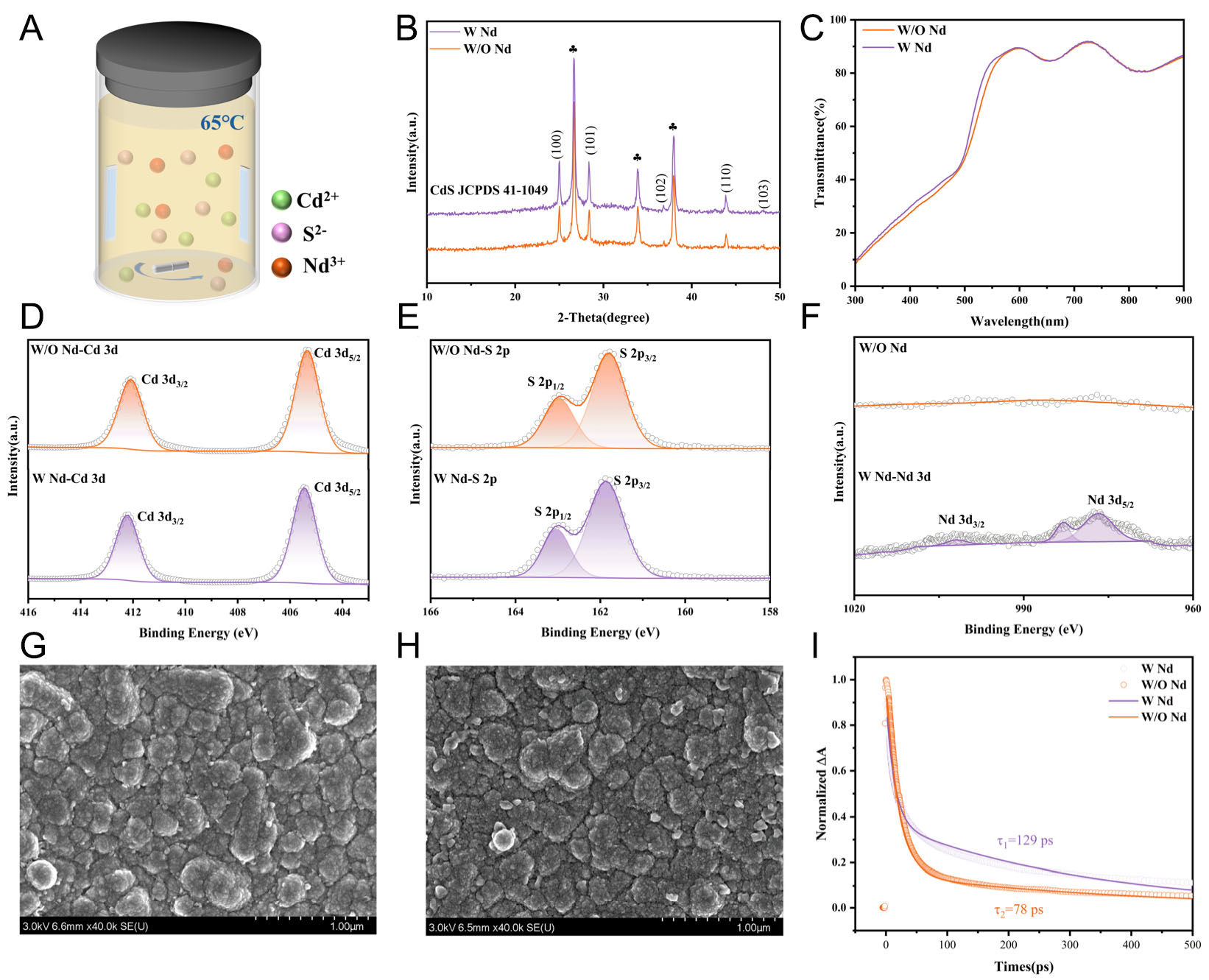
Figure 1. (A) Schematic diagram illustrating the deposition of Nd-incorporated CdS thin films, (B) XRD patterns of W Nd-CdS and W/O Nd-CdS samples, (C) Transmittance spectra, (D-F) XPS spectra of Cd 3d, S 2p, and Nd 3d, (G and H) Surface SEM images of W Nd-CdS and W/O Nd-CdS samples, (I) TAS spectra of W Nd-CdS and W/O Nd-CdS samples.
TAS was employed to measure minority carrier lifetime in CdS films. A 400 nm pulsed laser was used to excite the CdS surface, with delay times ranging from 0 to 6,000 ps. As shown in the TAS mapping images in Supplementary Figure 5A and B, the maximum absorption peak appears at 488 nm for W/O Nd and 502 nm for W Nd, indicating a red shift associated with bandgap variation. This shift is consistent with the morphology results, as SEM and AFM show markedly reduced particle features and decreased roughness after NdCl3 treatment, which lowers the spectral weighting of particle-related contributions and shifts the overall response toward the bulk CdS band-edge position[33]. Carrier decay curves at various wavelengths were extracted and fitted using a double-exponential model, as shown in Figure 1I. The relevant calculations are provided in Supplementary Note 1. The minority carrier lifetime increases from 78 ps for W/O Nd to 129 ps for W Nd, suggesting that NdCl3 treatment prolongs carrier migration and reduces surface defect density[34]. Delay time-dependent TA spectra are provided in Supplementary Figure 6.
Building on the previous systematic investigation of the effects of NdCl3 modification on the structural, morphological, and optoelectronic properties of CdS, we further explore whether and how this modification influences the crystallographic growth and preferred orientation of the subsequent Sb2Se3 absorber layer. Figure 2A-C illustrates the evolution of the Sb2Se3 absorber layer for the two sample sets: (a) under the W/O Nd condition, the Sb2Se3 nucleates with an essentially random orientation; (b-c) under the W Nd condition, Nd diffuses into Sb2Se3 during film growth, inducing a pronounced preferential [hk1] orientation. Figure 2D shows the XRD patterns of Sb2Se3 thin films grown under both conditions. The results indicate that the Sb2Se3 films grown under both conditions exhibit the same crystal structure, belonging to the orthorhombic system. A magnified view of the XRD patterns is provided in Supplementary Figure 7. The texture coefficients of the films were calculated from the XRD patterns, and the results are presented as a bar chart in Figure 2E. Since Sb2Se3 has a typical (Sb4Se6)n ribbon-like structure, the carrier transport is most efficient when the ribbon structure is perpendicular to the substrate, and least efficient when they are parallel[35]. The data show that Sb2Se3 films grown under the Nd treatment condition (W Nd) have higher texture coefficients on the (211), (221), and (301) planes compared to films grown without Nd (W/O Nd). This phenomenon indicates that the [hk1] orientation is favored during growth, which facilitates improved carrier transport (JCPDS card No. 15-0861). Figure 2F presents the Raman spectra of Sb2Se3 films with and without NdCl3 treatment. Two prominent peaks, located at approximately 188 and 208 cm-1, are observed. These peaks are typically attributed to the Sb-Se-Sb bending vibrations in the Sb2Se3 films[36,37]. The strengthened Raman features after Nd treatment suggest improved structural order and reduced defect-related disorder in the
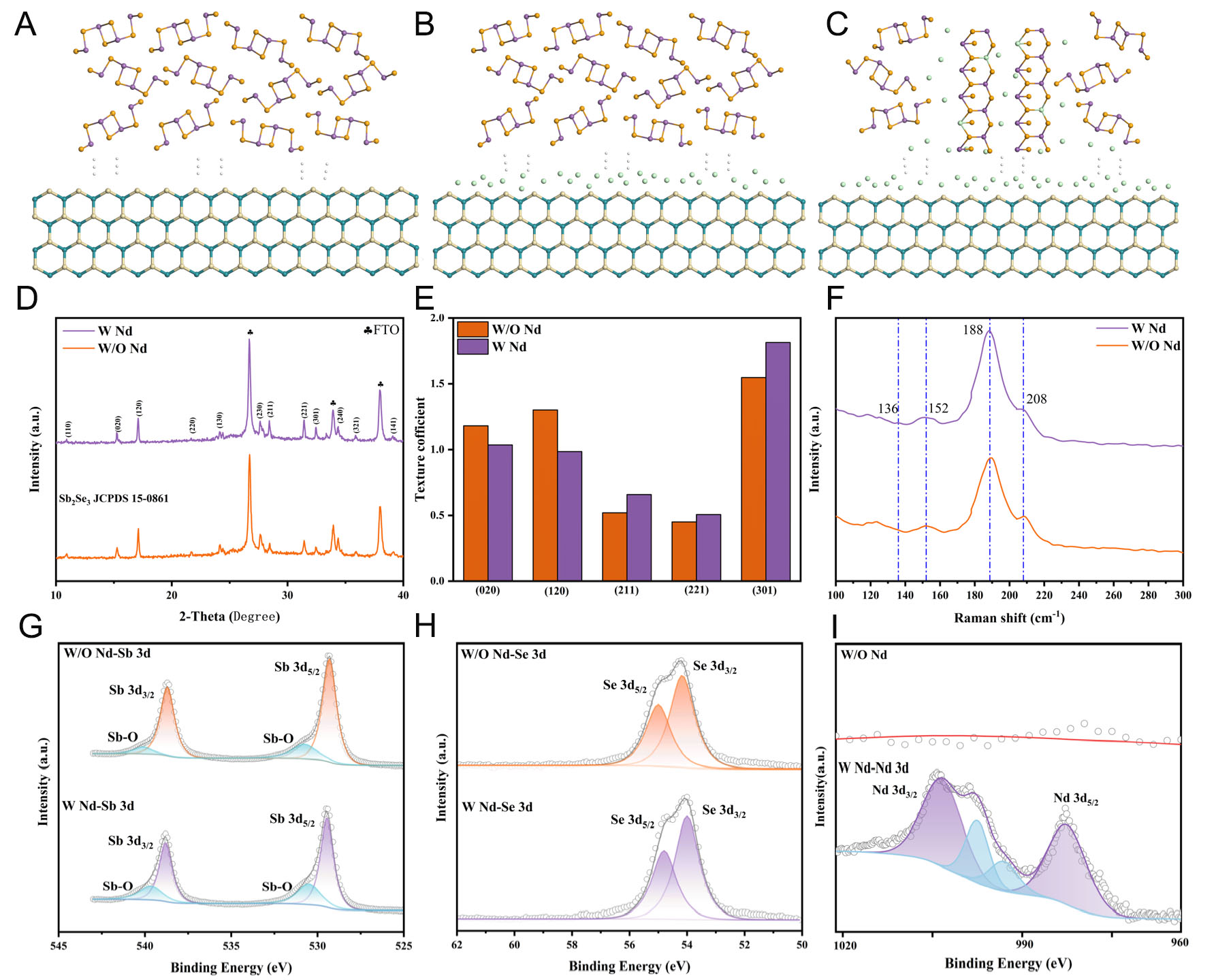
Figure 2. (A-C) Effect of W Nd-CdS and W/O Nd-CdS layers on the orientation of Sb2Se3 thin films, (D) XRD patterns of Sb2Se3 films with W Nd-CdS and W/O Nd-CdS layers, (E) Texture coefficients of Sb2Se3 films with W Nd-CdS and W/O Nd-CdS layers, (F) Raman spectra of Sb2Se3 films with W Nd-CdS and W/O Nd-CdS layers, (G-I) XPS spectra of Sb 3d, Se 3d, and Nd 3d for Sb2Se3 films prepared with
Figure 3A-D shows the relationship between the formation energy of point defects, where Nd substitutes for Sb, and the Fermi level under different chemical potential conditions (Sb-rich and Sb-poor). Lower formation energies indicate that a defect is more likely to form under a given Fermi level and chemical environment[39]. Under Sb-rich conditions [Figure 3A and B], the formation energy for Nd doping is significantly lower, suggesting that an Sb-rich environment is more favorable for Nd incorporation at the Sb site. This effect arises from the influence of the Sb chemical potential on the formation energy of Nd doping: in Sb-rich conditions, the higher Sb chemical potential reduces the energy barrier for Nd substitution at the Sb site. In contrast, under Sb-poor conditions [Figure 3C and D], the formation energy increases significantly, indicating that Sb-depleted environments are less favorable for Nd doping. The intersections of the curves corresponding to different charge states indicate the defect’s charge state transition points as the Fermi level varies. Under Sb-rich conditions (NdSb1), when the Fermi level increases from 0 eV (the valence band maximum) to approximately 0.5 eV, the Nd defect transitions from Nd3+ (high charge state) to Nd+ (low charge state). Similarly, under Sb-rich conditions (NdSb2), the transition from Nd3+ to Nd+ occurs around a Fermi level of 0.6 eV. These transition points suggest that under p-type conditions (low Fermi level), the high charge state (Nd3+) is more stable, while under n-type conditions (high Fermi level), the low charge state (such as Nd+ or Nd0) is more stable. Overall, the analysis indicates that Nd3+ doping has the lowest formation energy under Sb-rich conditions, making it more favorable for doping behavior. Additionally, a low Fermi level (p-type conditions) stabilizes the Nd3+ state, suggesting that Nd doping can be promoted by introducing an Sb-rich environment and controlling the Fermi level. It should be noted that, although hybrid functionals such as HSE06 may still underestimate absolute bandgap values compared with GW calculations or experimental results, the relative trends in defect formation energies and charge-state stability discussed here are expected to be robust with respect to the choice of exchange-correlation functional[40,41].
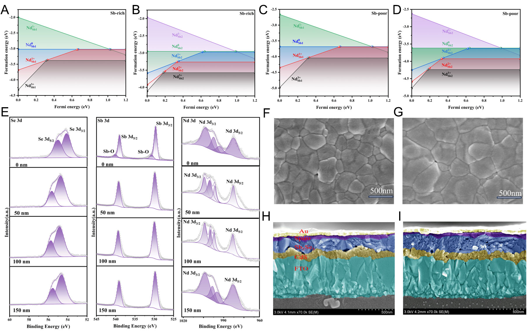
Figure 3. (A-D) Relationship between point defects and the Fermi level in Nd-doped Sb2Se3 thin films under different chemical potential conditions (Sb-rich and Sb-poor), (E) Variation in Se/Sb/Nd contents in Sb2Se3 samples at different etching depths, (F and G) Surface morphology of Sb2Se3 films with W Nd-CdS and W/O Nd-CdS, (H and I) Cross-sectional images of Sb2Se3 films with W Nd-CdS and W/O Nd-CdS.
Figure 3E presents the high-resolution depth-profile XPS spectra of NdCl3-treated Sb2Se3 films at etching depths of 0, 50, 100, and 150 nm. In the Se 3d region, the Se 3d5/2 and Se 3d3/2 peaks remain clearly defined across all depths, indicating a stable Se chemical state throughout the film. In the Sb 3d region, the main Sb 3d5/2 and Sb 3d3/2 peaks dominate, while a minor Sb-O shoulder is observed solely at the 0 nm depth, signifying surface-confined oxidation[42]. As the etching depth increases beyond 0 nm, the Sb-O component decreases rapidly, indicating that the bulk film is essentially unoxidized. In the Nd 3d region, clear Nd 3d peaks appear at each depth, and the Nd atomic concentration increases progressively with depth, thereby verifying that Nd diffuses inward from the heterojunction interface into the Sb2Se3 film rather than remaining as a superficial layer. To further investigate the effect of NdCl3 treatment on the morphology of Sb2Se3 films, surface SEM characterization was first performed. Figure 3F and G shows that the Sb2Se3 grains in the untreated sample are relatively small, whereas after introducing 0.05 mol L-1 NdCl3, the grain size increases significantly, indicating that NdCl3 treatment promotes grain growth. A more complete comparison of grain morphologies across the concentration series is provided in Supplementary Figure 8. The cross-sectional SEM images in Figure 3H and I further reveal that the Sb2Se3 film treated with NdCl3 exhibits a more compact columnar crystal structure, and the CdS/Sb2Se3 interface becomes smoother and more tightly packed; the visible gaps and voids within the film are markedly reduced, suggesting an overall improvement in film continuity and structural quality. To further verify this trend, we conducted AFM measurements on the samples with and without NdCl3 treatment. Supplementary Figure 9A and B shows that NdCl3 treatment reduces the surface roughness (Ra) of the Sb2Se3 film from 26.3 to 23.7 nm, further confirming enhanced surface flatness and uniformity. Taken together, these results indicate that NdCl3 treatment improves the compactness of the CdS/Sb2Se3 interface, enhances the crystallinity of Sb2Se3, and consequently reduces both interfacial and bulk defect densities, thereby laying the foundation for improved device performance.
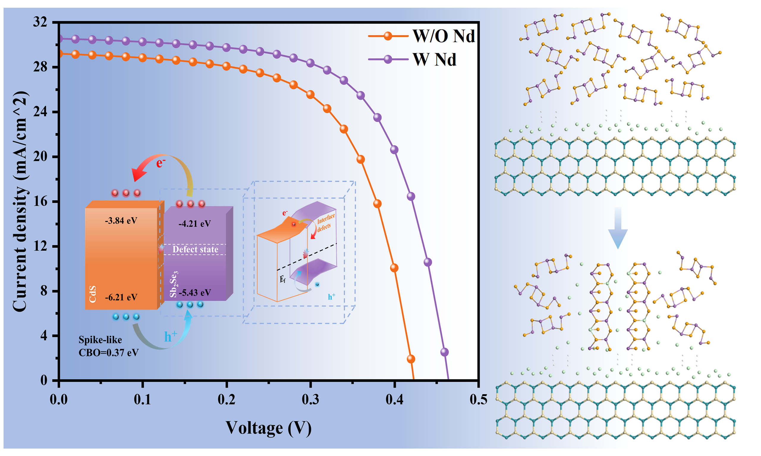
To clarify how Nd doping modulates the interfacial band characteristics of the CdS/Sb2Se3 heterojunction, KPFM measurements were conducted. As shown in Figure 4A and B, the untreated Sb2Se3 film exhibits a low and spatially nonuniform contact potential difference (CPD), whereas the Nd-treated sample presents a significantly higher and more uniform CPD distribution, indicating reduced surface defect density and enhanced electronic homogeneity[43]. The line-scan profiles in Figure 4C and D further confirm that local CPD fluctuations are substantially suppressed after Nd incorporation, reflecting a more uniform surface work function. The CPD histograms in Figure 4E and F show that the untreated sample exhibits a large surface photovoltage (SPV≈122 mV), whereas the Nd-treated film displays a substantially reduced SPV
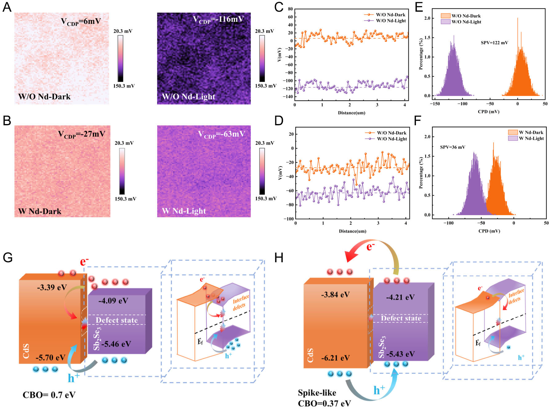
Figure 4. (A) CPD maps of W/O Nd-CdS Sb2Se3 thin films under dark and illuminated conditions, (B) CPD maps of W Nd-CdS Sb2Se3 thin films under dark and illuminated conditions, (C) Surface potential maps of W/O Nd-CdS Sb2Se3 thin films under dark and illuminated conditions, (D) Surface potential maps of W Nd-CdS Sb2Se3 thin films under dark and illuminated conditions, (E and F) SPV images of W/O Nd-CdS and W Nd-CdS Sb2Se3 thin films, (G and H) Schematic diagrams of energy band alignment and carrier transport mechanisms in W/O Nd-CdS and W Nd-CdS CdS/Sb2Se3 heterojunctions.
In conjunction with the KPFM analysis, the optical properties and band structures of CdS and Sb2Se3 were systematically examined to elucidate the impact of NdCl3 treatment. Ultraviolet-visible (UV-vis) measurements [Supplementary Figure 10A] show that NdCl3-treated Sb2Se3 exhibits enhanced absorption across 400-1,000 nm, suggesting improved photon utilization and more efficient photocarrier generation[44]. Tauc analysis reveals that the bandgaps of untreated and Nd-treated CdS films are 2.31 and 2.38 eV, respectively, whereas those of Sb2Se3 are 1.34 and 1.22 eV [Supplementary Figure 10B]. UPS measurements further provide the Fermi level and valence band maximum positions for each sample
Figure 5A displays the J-V results of devices with and without NdCl3 treatment. Table 1 lists the specific photovoltaic device parameters. After NdCl3 treatment, the short-circuit current density (JSC), open-circuit voltage (VOC), and fill factor (FF) were 30.54 mA/cm2, 0.465 V, and 64.58%, respectively. Additionally, a maximum PCE of 9.17% is achieved. In contrast, the untreated devices exhibited JSC, VOC, FF, and PCE values of 28.60 mA/cm2, 0.424 V, 62.27%, and 7.55%, respectively. Figure 5B presents the EQE values for both devices. The integrated JSC values, calculated according to Supplementary Note 3 based on EQE integration, were 28.50 and 26.02 mA/cm2 for the devices with and without NdCl3 treatment, respectively, closely matching the JSC values obtained from the J-V curves. Furthermore, the EQE results indicate an enhanced optical response at long wavelengths for NdCl3-treated devices, suggesting reduced recombination and efficient charge collection[46]. Table 2 and Figure 5C depict the dark current-voltage (IV) results of the two devices. The parameters were derived according to Supplementary Note 4, using the diode single-exponential equation. From the dJ/dV vs. V plot [Figure 5D], the conductance (G) values for the device without and with the element Nd were 4.93 × 10⁻² and 3.10 × 10⁻³ mS/cm2, respectively, indicating that the Nd-treated device has a higher parallel resistance[47,48]. The corresponding resistance (R) and ideality factor (A) values can be obtained from the
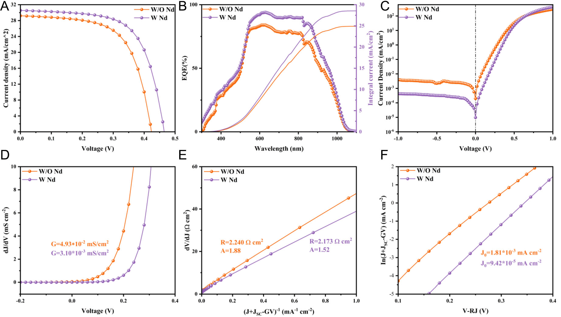
Figure 5. (A) J-V curves, (B) EQE spectra, (C) dark J-V curves, (D) dJ/dV vs. V graph for G extraction, (E) dV/dJ vs. (J + JSC - GV)-1 graph for R and A extraction, and (F) ln(J + JSC - GV) vs. V-RJ graph for J0 extraction, for samples without and with NdCl3 treatment.
The photovoltaic parameters of Sb2Se3 solar cells without and with NdCl3 treatment
| Sample | VOC (V) | JSC (mA/cm2) | FF (%) | Efficiency (%) | RS (ohm) | RSH (ohm) |
| W/O Nd | 0.424 | 28.60 | 62.27 | 7.55 | 114.83 | 13,014 |
| W Nd | 0.465 | 30.54 | 64.58 | 9.17 | 110.48 | 19,782 |
Electrical parameters related to the diode and interface for devices without and with NdCl3 treatment
| Sample | G (mS/cm2) | R (Ω cm2) | A | J0 (mA/cm2) | Wd (nm) | Ntrap (cm-3) |
| W/O Nd | 4.93 × 10⁻² | 2.24 | 1.88 | 1.81 × 10⁻³ | 216.44 | 2.98 × 10¹⁴ |
| W Nd | 3.10 × 10⁻³ | 2.173 | 1.52 | 9.42 × 10⁻⁵ | 307.60 | 1.76 × 10¹⁴ |
To better understand the factors contributing to the differences in carrier lifetimes, capacitance-voltage (C-V) analysis was also performed in this study. As shown in Figure 6A, the Mott-Schottky curves (1/C2-V) indicate that the built-in voltage of the W/O Nd device is 0.474 V, while that of the W Nd device is 0.530 V. The increased built-in electric field provides a greater driving force for carrier separation, resulting in faster charge separation[51]. The parameters were calculated according to Supplementary Note 5 using the C-V fitting method to extract the depletion width. The depletion widths (Wd) of the W/O Nd and W Nd devices were calculated to be 216.44 and 307.60 nm, respectively [Figure 6B]. A narrower depletion width indicates a significant tunneling effect and insufficient carrier separation, which leads to a higher VOC deficit in the W/O Nd device[52]. Figure 6C presents the EIS results for both devices. A similar circuit model was employed to effectively fit the impedance results. Compared to the deposited samples, the RS value of the device after NdCl3 treatment decreases, while the charge transfer resistance (Rrec) value increases, indicating enhanced carrier transport and inhibited carrier recombination. Figure 6D and E shows the space-charge-limited current (SCLC) dark logarithmic J-V curves of the two devices. The calculated onset voltages in the trap-filled limit (TFL) region (VTFL) for the untreated and treated devices are 0.54 and 0.32 V, respectively. The defect density was calculated according to Supplementary Note 6 based on the VTFL analysis.
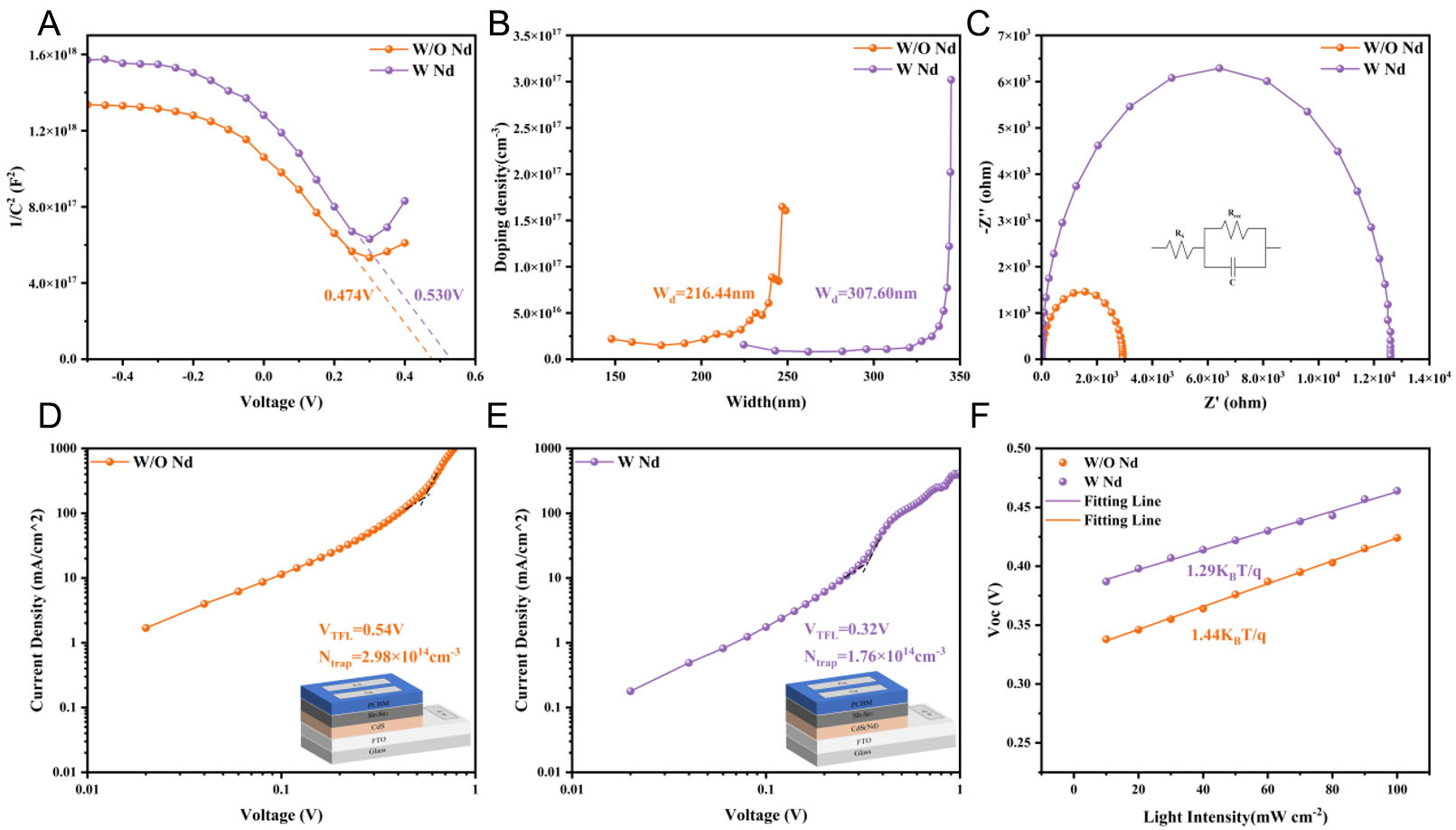
Figure 6. (A) Mott-Schottky plots (1/C2-V), (B) NC-V curves, (C) Nyquist plots, (D and E) space-charge-limited current (SCLC) measurements of W/O and W Nd samples, (F) light-intensity dependence of VOC.
The extracted Ntrap values for the control and Nd-doped Sb2Se3 films are 2.98 × 10¹⁴ and 1.76 × 1014 cm-3, respectively. The reduced trap density in the Nd-doped Sb2Se3 film indicates a lower concentration of electrically active defects, which is consistent with the suppression of trap-assisted recombination[53]. As shown in Figure 6F, the slope obtained from the linear fitting is mainly associated with trap-assisted Shockley-Read-Hall (SRH) recombination. Compared with the control device, the NdCl3-treated device exhibits a significantly lower slope, suggesting that SRH recombination is effectively suppressed, thereby contributing to improved device performance[54,55]. To further evaluate the stability of Sb2Se3 solar cells, additional aging tests were conducted under controlled conditions with a temperature of 25 °C and a relative humidity of 35% ± 5% [Supplementary Figure 13]. Compared with the control device, the NdCl3-treated Sb2Se3 device demonstrates a longer carrier lifetime and a more stable PCE. This behavior reflects more efficient charge extraction and collection, as well as a reduced recombination rate in the NdCl3-treated Sb2Se3 film[56,57]. Overall, these results demonstrate that Nd doping effectively reduces defect density, suppresses charge recombination, and enhances carrier separation and transport, leading to improved efficiency and stability of Sb2Se3 solar cells.
CONCLUSIONS
In summary, this study proposes an Nd-based ionic antisite diffusion strategy to regulate the growth and interfacial properties of Sb2Se3 thin films. The controlled diffusion of Nd contributes to enhanced structural order, regulated orientation and grain evolution, reduced defect-related disorder, and a more favorable interfacial energy structure, thereby facilitating more effective charge transport and recombination suppression in the device. These findings indicate that rare-earth-mediated diffusion engineering represents a viable approach for addressing key materials and interface challenges in Sb2Se3-based devices. More broadly, this work provides a conceptual framework for the application of ionic diffusion control in Q1D semiconductors and may inform future design strategies for high-performance photovoltaic devices.
DECLARATIONS
Authors’ contributions
Conducted the majority of the experiments, performed data analysis, and wrote the manuscript: Dong, X.; Deng, W.; Zhi, Y.
Contributed to experimental fabrication and characterization: Shen, B.; Li, S.; Tang, C.
Performed first-principles calculations and theoretical analysis: Lu, M.
Assisted in experimental work and data interpretation: Jiang, S.
Contributed to experimental implementation: Qiu, J.
Performed device testing and characterization: Li, L.
Supervised the experimental work, secured funding, and contributed to writing and revising the manuscript: Guo, H.
Assisted in experiments and contributed to manuscript revision: Yuan, N.
Supervised the project, secured funding, and contributed to manuscript revision: Ding, J.
Availability of data and materials
The data supporting the findings of this study are available from the corresponding author upon reasonable request.
AI and AI-assisted tools statement
Not applicable.
Financial support and sponsorship
This work was supported by Changzhou University, the National Science Foundation of China (Grant No. 62504024, 62504023, 12202078), China Postdoctoral Science Foundation (Certificate No. 2025M770524), the Natural Science Foundation of Jiangsu Province (Grant No. BK20220624), the Changzhou Sci & Tech Program (Grant No. CJ20241086), the Natural Science Foundation of Yangzhou (YZ2024177), and the Yangzhou Innovation Capability Enhancement Program (YZ2022170).
Conflicts of interest
Cheng Tang is affiliated with the Technology Development Department, Avicas Generic Technology Co., Ltd. The other authors declared that there are no conflicts of interest.
Ethical approval and consent to participate
Not applicable.
Consent for publication
Not applicable.
Copyright
© The Author(s) 2026.
Supplementary Materials
REFERENCES
1. Wen, X.; Chen, C.; Lu, S.; et al. Vapor transport deposition of antimony selenide thin film solar cells with 7.6% efficiency. Nat. Commun. 2018, 9, 2179.
2. Li, Z.; Liang, X.; Li, G.; et al. 9.2%-efficient core-shell structured antimony selenide nanorod array solar cells. Nat. Commun. 2019, 10, 125.
3. Wang, L.; Li, D.; Li, K.; et al. Stable 6%-efficient Sb2Se3 solar cells with a ZnO buffer layer. Nat. Energy. 2017, 2, 17046.
4. Chen, C.; Li, K.; Chen, S.; et al. Efficiency improvement of Sb2Se3 solar cells via grain boundary inversion. ACS. Energy. Lett. 2018, 3, 2335-41.
5. Zhao, Y.; Wang, S.; Li, C.; et al. Regulating deposition kinetics via a novel additive-assisted chemical bath deposition technology enables fabrication of 10.57%-efficiency Sb2Se3 solar cells. Energy. Environ. Sci. 2022, 15, 5118-28.
6. Zhu, P.; Chen, C.; Dai, J.; et al. Toward the commercialization of perovskite solar modules. Adv. Mater. 2024, 36, e2307357.
7. Shah, U. A.; Wang, A.; Irfan, Ullah. M.; et al. A deep dive into Cu2ZnSnS4 (CZTS) solar cells: a review of exploring roadblocks, breakthroughs, and shaping the future. Small 2024, 20, e2310584.
8. Wijesinghe, U.; Longo, G.; Hutter, O. S. Defect engineering in antimony selenide thin film solar cells. Energy. Adv. 2023, 2, 12-33.
9. Ma, Y.; Tang, B.; Lian, W.; et al. Efficient defect passivation of Sb2Se3 film by tellurium doping for high performance solar cells. J. Mater. Chem. A. 2020, 8, 6510-6.
10. Wang, Z.; Bae, S.; Baljozović, M.; et al. One-step hydrothermal synthesis of Sn-doped Sb2Se3 for solar hydrogen production. ACS. Catal. 2024, 14, 9877-86.
11. Ramírez-Velasco, S.; González-Castillo, J.; Ayala-Mató, F.; Hernández-Calderón, V.; Jiménez-Olarte, D.; Vigil-Galán, O. Back contact modification in Sb2Se3 solar cells: the effect of a thin layer of MoSe2. Thin. Solid. Films. 2022, 751, 139227.
12. Zhao, Q.; Che, B.; Wang, H.; et al. Crystal reconstruction and defect healing enabled high-quality Sb2Se3 films for solar cell applications. J. Mater. Chem. A. 2024, 12, 11524-34.
13. Jakomin, R.; Rampino, S.; Spaggiari, G.; Pattini, F. Advances on Sb2Se3 solar cells fabricated by physical vapor deposition techniques. Solar 2023, 3, 566-95.
14. Zhao, Q.; Tang, R.; Yang, S.; Chen, T. Post-treatment strategies toward high-quality Sb2Se3 thin films in photovoltaic applications. Adv. Sci. 2025, 12, e11387.
15. Che, B.; Cai, Z.; Xu, H.; et al. Post-deposition treatment of Sb2Se3 enables defect passivation and increased carrier transport dimension for efficient solar cell application. Angew. Chem. Int. Ed. 2025, 64, e202425639.
16. Otavio Mendes, J.; Merenda, A.; Wilson, K.; Fraser Lee, A.; Della Gaspera, E.; van Embden, J. Substrate morphology directs (001) Sb2Se3 thin film growth by crystallographic orientation filtering. Small 2024, 20, e2302721.
17. Liang, X.; Feng, Y.; Dang, W.; et al. High-efficiency flexible Sb2Se3 solar cells by back interface and absorber bulk deep-level trap engineering. ACS. Energy. Lett. 2022, 8, 213-21.
18. Pasini, S.; Spoltore, D.; Parisini, A.; et al. Innovative back-contact for Sb2Se3-based thin film solar cells. Sol. Energy. 2023, 249, 414-23.
19. Guo, H.; Huang, S.; Zhu, H.; et al. Enhancement in the efficiency of Sb2Se3 solar cells by triple function of lithium hydroxide modified at the back contact interface. Adv. Sci. 2023, 10, e2304246.
20. Hoang, V.; Lee, J.; Lim, G.; et al. Interface engineering of co-evaporated Sb2Se3 solar cells using an ALD SnOx interlayer. EES. Sol. 2025, 1, 990-1003.
21. Spalatu, N.; Krautmann, R.; Katerski, A.; et al. Screening and optimization of processing temperature for Sb2Se3 thin film growth protocol: Interrelation between grain structure, interface intermixing and solar cell performance. Sol. Energy. Mater. Sol. Cells. 2021, 225, 111045.
22. Hanifehpour, Y.; Joo, S. W.; Min, B. K. Lu3+/Yb3+ and Lu3+/Er3+ co-doped antimony selenide nanomaterials: synthesis, characterization, and electrical, thermoelectrical, and optical properties. Nanoscale. Res. Lett. 2013, 8, 141.
23. Parnicka, P.; Mazierski, P.; Grzyb, T.; et al. Influence of the preparation method on the photocatalytic activity of Nd-modified TiO2. Beilstein. J. Nanotechnol. 2018, 9, 447-59.
24. Alemi, A.; Hanifehpour, Y.; Joo, S. W.; Min, B.; Oh, T. H. Structural studies and optical and electrical properties of novel Gd3+-doped Sb2Se3 nanorods. J. Nanomater. 2012, 2012, 983150.
25. Ruiz-Ortega, R. C.; Esquivel-Mendez, L. A.; Gonzalez-Trujillo, M. A.; Hernandez-Vasquez, C.; Matsumoto, Y.; Albor-Aguilera, M. L. Comprehensive analysis of CdS ultrathin films modified by the substrate position inside the reactor container using the CBD technique. ACS. Omega. 2023, 8, 31725-37.
26. Najm, A. S.; Naeem, H. S.; Majdi, H. S.; et al. An in-depth analysis of nucleation and growth mechanism of CdS thin film synthesized by chemical bath deposition (CBD) technique. Sci. Rep. 2022, 12, 15295.
27. Safi, A. A.; Ibrahim, I. M. The effect of rare-earth doping on CdS nanostructure: structural, optical and photoconductivity properties. Iraqi. J. Phys. 2019, 17, 108-18.
28. Kausar, R.; Khan, M. A.; Rasool, R. T.; Arshad, M.; Ashraf, G. A. Structural, morphological, spectral, XPS, and dielectric properties of Ba4Co2NdxFe36-xO60 nanocrystalline materials. Chem. Pap. 2024, 78, 5349-66.
29. Zhang, Y.; Ran, X.; Fu, H.; et al. Band alignment tunning via the facets of CdS nanocrystals with g-C3N4 for unveiling their enhanced photocatalytical property. Adv. Funct. Mater. 2024, 34, 2404585.
30. Yang, W.; Kim, J. H.; Hutter, O. S.; et al. Benchmark performance of low-cost Sb2Se3 photocathodes for unassisted solar overall water splitting. Nat. Commun. 2020, 11, 861.
31. Li, J.; Zhao, Y.; Li, C.; et al. Hydrazine hydrate-induced surface modification of CdS electron transport layer enables 10.30%-efficient Sb2(S,Se)3 planar solar cells. Adv. Sci. 2022, 9, 2202356.
32. Wang, X.; Guo, H.; Chen, Z.; et al. Enhancement of Sb2Se3 thin-film solar cell photoelectric properties by addition of interlayer CeO2. Solar. Energy. 2019, 188, 218-23.
33. Qi, L.; Cölfen, H.; Antonietti, M. Synthesis and characterization of CdS nanoparticles stabilized by double-hydrophilic block copolymers. Nano. Lett. 2000, 1, 61-5.
34. Gu, Y.; Liang, W.; Che, Y.; et al. Solvent annealing enabling reconstruction of cadmium sulfide film for improved heterojunction quality and photovoltaic performance of antimony selenosulfide solar cells. Adv. Funct. Mater. 2023, 34, 2311577.
35. Zhou, J.; Meng, D.; Yang, T.; et al. Enhanced charge carrier transport via efficient grain conduction mode for Sb2Se3 solar cell applications. Appl. Surf. Sci. 2022, 591, 153169.
36. Li, Z.; Chen, X.; Zhu, H.; et al. Sb2Se3 thin film solar cells in substrate configuration and the back contact selenization. Sol. Energy. Mater. Sol. Cells. 2017, 161, 190-6.
37. Liang, G.; Luo, Y.; Chen, S.; et al. Sputtered and selenized Sb2Se3 thin-film solar cells with open-circuit voltage exceeding 500 mV. Nano. Energy. 2020, 73, 104806.
38. Mohamed, N. A.; Kiong, T. S.; Ismail, A. F. Revolutionizing water splitting: the role of light rare earth elements (LREEs) in photoelectrochemical and electrochemical advances. Coord. Chem. Rev. 2025, 543, 216917.
39. Cai, Z.; Che, B.; Gu, Y.; et al. Active passivation of anion vacancies in antimony selenide film for efficient solar cells. Adv. Mater. 2024, 36, e2404826.
40. Janesko, B. G. Replacing hybrid density functional theory: motivation and recent advances. Chem. Soc. Rev. 2021, 50, 8470-95.
41. Shinde, R.; Yamijala, S. S. R. K. C.; Wong, B. M. Improved band gaps and structural properties from Wannier-Fermi-Löwdin self-interaction corrections for periodic systems. J. Phys. Condens. Matter. 2021, 33, 115501.
42. Mo, Y.; Li, C.; Yang, J.; et al. High-efficiency all-antimony chalcogenide tandem solar cells via thermal-evaporated CdS interface engineering. Adv. Mater. 2025, 37, e06372.
43. Chen, S.; Wang, X.; Chen, X.; et al. Self-regulated growth of large-grain Sb2Se3 thin films for high-efficiency solar cells. Adv. Funct. Mater. 2024, 34, 2402978.
44. Liu, Z.; Wang, L.; Yu, X.; et al. Piezoelectric-effect-enhanced full-spectrum photoelectrocatalysis in p-n heterojunction. Adv. Funct. Mater. 2019, 29, 1807279.
45. Li, Y.; Wang, K.; Huang, D.; et al. CdxZn1-xS/Sb2Se3 thin film photocathode for efficient solar water splitting. Appl. Catal. B. Environ. 2021, 286, 119872.
46. Yang, Y.; Zhang, T.; Zhu, H.; et al. Optimizing crystal orientation and defect mitigation in antimony selenide thin-film solar cells through buffer layer energy band adjustment. Small 2024, 20, e2403292.
47. Shen, K.; Zhang, Y.; Wang, X.; et al. Efficient and stable planar n-i-p Sb2Se3 solar cells enabled by oriented 1D trigonal selenium structures. Adv. Sci. 2020, 7, 2001013.
48. Zhang, T.; Yang, Y.; Dong, J.; et al. Regulation of the charge carrier dynamics in antimony selenide thin-film solar cells based on the effective diffusion of ions at the heterojunction interface. Adv. Funct. Mater. 2024, 35, 2417868.
49. Santakrus Singh, N.; Jain, A.; Kapoor, A. Determination of the solar cell junction ideality factor using special trans function theory (STFT). Sol. Energy. Mater. Sol. Cells. 2009, 93, 1423-6.
50. Chen, S.; Ye, Y. A.; Ishaq, M.; et al. Simultaneous band alignment modulation and carrier dynamics optimization enable highest efficiency in Cd-free Sb2Se3 solar cells. Adv. Funct. Mater. 2024, 34, 2403934.
51. Chen, G.; Zhao, J.; Chen, S.; et al. Perspective of environmentally friendly antimony selenide-based solar cell. Appl. Phys. Lett. 2024, 125, 200502.
52. Chen, S.; Fu, Y.; Ishaq, M.; et al. Carrier recombination suppression and transport enhancement enable high-performance self-powered broadband 3 photodetectors. InfoMat 2023, 5, e12400.
53. Yang, J.; Chen, M.; Chen, G.; et al. Back interface and absorber bulk deep-level trap optimization enables highly efficient flexible antimony triselenide solar cell. Adv. Sci. 2024, 11, e2310193.
54. Chen, X.; Zhao, Y.; Li, C.; et al. Interfacial engineering by self-assembled monolayer for high-performance Sb2S3 solar cells. Adv. Energy. Mater. 2024, 14, 2400441.
55. Li, K.; Yang, J.; Cai, Z.; et al. Effect of energy-driven molecular precursor decomposition on the crystal orientation of antimony selenide film and solar cell efficiency. Small. Method. 2024, 8, e2400227.
56. Wang, S.; Zhao, Y.; Che, B.; et al. A novel multi-sulfur source collaborative chemical bath deposition technology enables 8%-efficiency Sb2S3 planar solar cells. Adv. Mater. 2022, 34, e2206242.
Cite This Article
How to Cite
Download Citation
Export Citation File:
Type of Import
Tips on Downloading Citation
Citation Manager File Format
Type of Import
Direct Import: When the Direct Import option is selected (the default state), a dialogue box will give you the option to Save or Open the downloaded citation data. Choosing Open will either launch your citation manager or give you a choice of applications with which to use the metadata. The Save option saves the file locally for later use.
Indirect Import: When the Indirect Import option is selected, the metadata is displayed and may be copied and pasted as needed.
About This Article
Special Topic
Copyright

Data & Comments
Data
0


Comments
Comments must be written in English. Spam, offensive content, impersonation, and private information will not be permitted. If any comment is reported and identified as inappropriate content by OAE staff, the comment will be removed without notice. If you have any queries or need any help, please contact us at [email protected].