


fig4
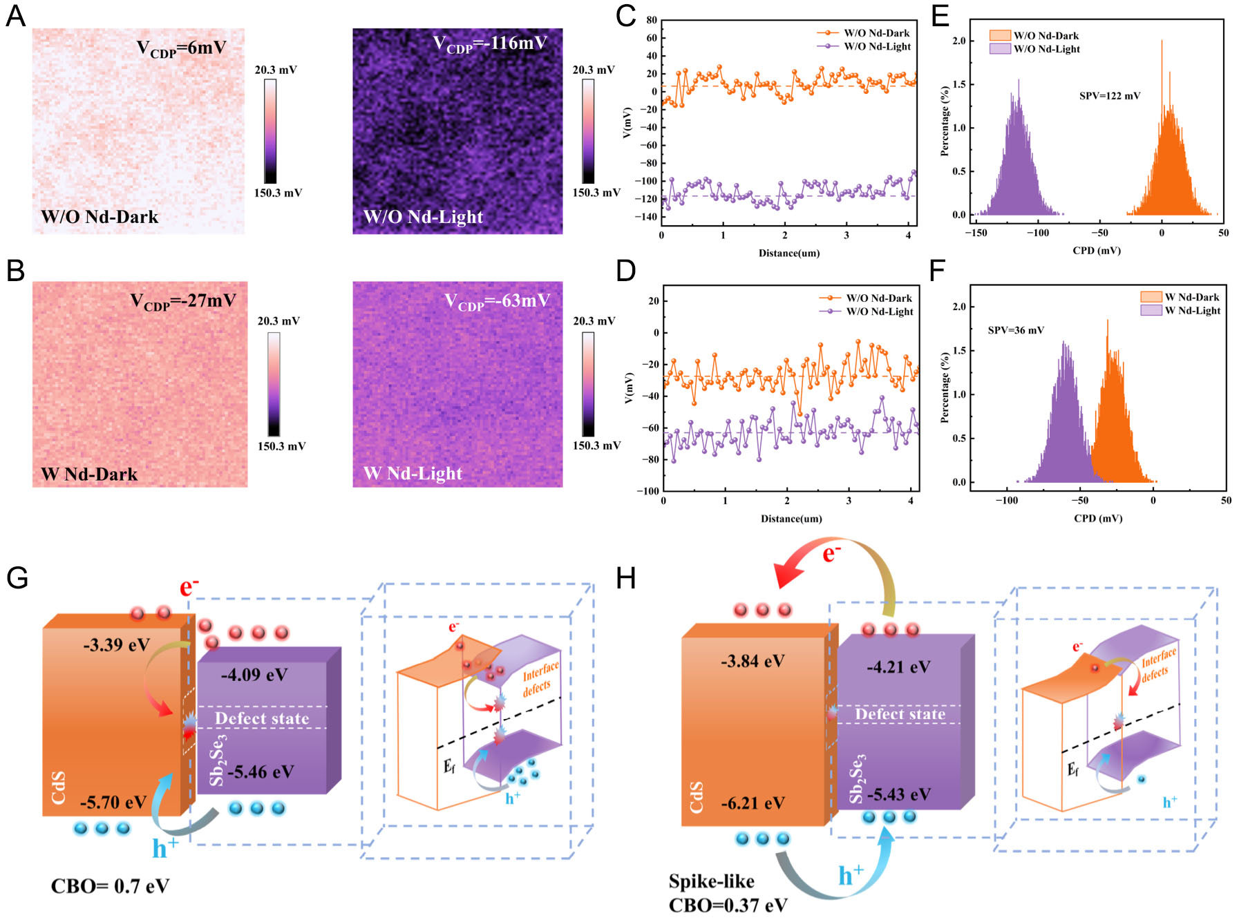
Figure 4. (A) CPD maps of W/O Nd-CdS Sb2Se3 thin films under dark and illuminated conditions, (B) CPD maps of W Nd-CdS Sb2Se3 thin films under dark and illuminated conditions, (C) Surface potential maps of W/O Nd-CdS Sb2Se3 thin films under dark and illuminated conditions, (D) Surface potential maps of W Nd-CdS Sb2Se3 thin films under dark and illuminated conditions, (E and F) SPV images of W/O Nd-CdS and W Nd-CdS Sb2Se3 thin films, (G and H) Schematic diagrams of energy band alignment and carrier transport mechanisms in W/O Nd-CdS and W Nd-CdS CdS/Sb2Se3 heterojunctions.


