


High-efficiency solar-to-hydrogen conversion via MoS2-enhanced GaAs heterojunctions for efficient photoelectrochemical water splitting
 0
0 Abstract
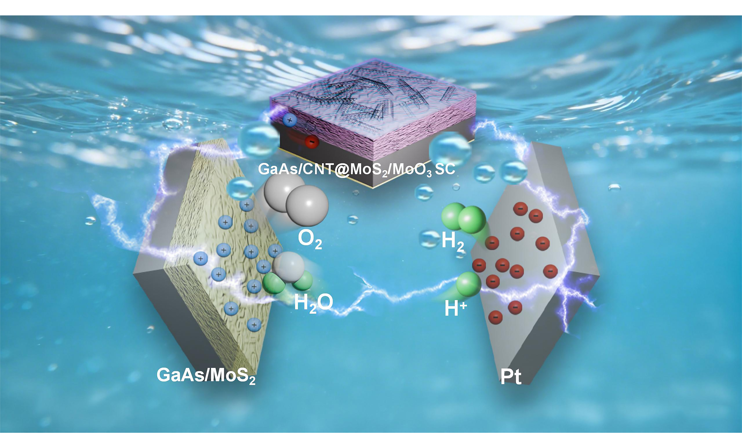
Gallium arsenide (GaAs) heterojunctions have been widely explored for their promising applications in solar cells (SCs) and photoelectrochemical (PEC) water splitting, owing to their cost-effective design and great potential for enhancing power conversion efficiency (PCE). In this study, an innovative MoS2 hole-transport layer was introduced into the GaAs heterojunction for applications in SCs and PEC water splitting. By optimizing the thickness of the MoS2 film, the sulfide oxidation reaction at the heterointerface was effectively suppressed. Significantly, a synergistic system integrating a GaAs heterojunction SC with a photoelectrode was proposed. The incorporation of carbon nanotubes into the GaAs/MoS2 heterojunction significantly improved charge carrier transport, enhancing the PCE from 0.24% to 12.41%. In the PEC water splitting system, the GaAs/MoS2 heterostructure also demonstrated excellent oxygen evolution reaction performance. This optimization led to a maximum applied bias photon-to-current efficiency of 35% under bias, reaching 20% at 0 V vs. reversible hydrogen electrode (RHE), along with a photocurrent density of 40 mA cm-2 and a solar-to-hydrogen conversion efficiency of 17.22%. When integrated into a photovoltaic-PEC system, the GaAs/MoS2 photoelectrode achieved a current density of 20 mA cm-2 at 0 V vs. RHE, with a 400 mV negative shift in the water oxidation onset potential, enabling highly efficient solar-driven hydrogen production.
Keywords
INTRODUCTION
The replacement of traditional fossil fuels with green energy sources has become imperative, and the advancement of solar-to-hydrogen (STH) energy conversion technologies has garnered significant research attention. Photoelectrochemical (PEC) water splitting offers a promising alternative to conventional electrolysis by directly using solar energy as the input, thereby avoiding electricity as an intermediate energy carrier and reducing both fossil fuel dependence and operational costs[1]. A wide range of materials have been explored for PEC applications, including metal oxides (e.g., TiO2[2], α-Fe2O3[3], WO3[4], BiVO4[5], ZnO[6]) and nitrides (e.g., Ta3N5[7], BaTaO2N[8], g-C3N4[9]) as photoanodes for oxygen evolution, as well as cathodes such as Si[10], InP[11], and various metal oxides/sulfides/selenides (e.g., Cu2O[12], CdTe[13], CuFeO2[14]) for hydrogen evolution. A fundamental challenge, however, lies in simultaneously achieving high efficiency, stability, and low cost. While metal oxides are typically stable, they often suffer from limited efficiency. Conversely, highly efficient materials such as III-V compounds are usually costly or unstable. Consequently, research efforts are dedicated to advanced material engineering strategies, including nanostructuring[15], doping[16], heterojunction formation[17], and co-catalyst integration[18], tailored to improve light harvesting, charge carrier separation, and surface reaction kinetics. The ultimate objective is to overcome the barriers to the practical implementation of PEC technology.
Gallium arsenide (GaAs), characterized by its near-ideal bandgap, high light absorption coefficient, and excellent theoretical power conversion efficiency (PCE), has found extensive application in the photovoltaic (PV) field[19]. Beyond its capability for high-efficiency solar energy harvesting and conversion into electricity, GaAs also plays a critical role in catalyzing the water oxidation reaction, enabling efficient oxygen evolution. These combined attributes render it an ideal high-performance photoanode material, serving as a promising alternative to conventional photoelectrodes. Consequently, several GaAs-based photoanodes have been developed for PEC hydrogen generation, exemplified by structures such as
To address this, researchers have proposed GaAs heterojunction configurations. Currently, studies have successively reported on GaAs/ZnO (8.75%)[22], GaAs/PEDOT:PSS (15.08%)[23], GaAs/MoS2 (9.03%)[24], GaAs/CuI (13.42%)[25], GaAs/Graphene (18.5%)[26,27] and GaAs/carbon nanotube (CNT, 11.24%)[28] heterojunctions have been used in solar cells (SCs). Among various strategies, the construction of heterojunctions by coupling GaAs light-absorbing layers with carrier transport films composed of the aforementioned inorganic compounds, organic substances, and carbon materials represents a promising alternative to traditional III-V compound semiconductor homojunctions. This strategy not only maintains high efficiency but also further simplifies device fabrication processes and equipment requirements, while reducing both manufacturing and application costs. Notably, several GaAs-based heterojunction photoanodes have been reported to date, including GaAs/InS[29], GaAs/TiO2[30]and GaAs/carbon nanotube/graphene oxide (CNTGO)[31]. In our previous studies[31,32], we have successfully demonstrated that heterojunctions constructed by combining CNT hole transport films with GaAs can exhibit excellent PV and PEC water splitting performance. Nevertheless, inherent chemical inertness of pristine carbon-based transport layers can partially impede interfacial charge-injection kinetics, thereby limiting further enhancement of the STH conversion efficiency. Moreover, single photoelectrode systems face inherent limitations such as narrow spectral absorption, significant bulk and surface recombination, insufficient PV for unassisted water splitting, and poor operational stability[30]. Consequently, the development of highly electroactive photoelectrodes and their monolithic integration with PV units is essential to overcome the performance bottlenecks of standalone PEC systems.
In this study, GaAs/MoS2 heterojunctions were successfully fabricated using a combination of vacuum filtration, magnetron sputtering and chemical vapor deposition (CVD). The constructed GaAs/CNT@MoS2 heterojunction solar cell (HJSC) achieved a notable PCE of up to 12.41%. Furthermore, the GaAs/MoS2 heterojunction demonstrated exceptional performance as a photoelectrode for PEC water splitting, ultimately achieving a STH conversion efficiency of 17.22%. Applied bias photon-to-current efficiency (ABPE) measurements showed that the GaAs/MoS2 heterojunctions achieved a maximum value of 35% under applied bias, and maintained 20% even at 0 V vs. the reversible hydrogen electrode (RHE), highlighting their capability for bias-free operation. Moreover, an integrated PV-PEC system was constructed by connecting the optimized GaAs/CNT@MoS2/MoO3 HJSC in series with the GaAs/MoS2 photoanode. This system delivered a current density of 20 mA cm-2 at 0 V vs. RHE, demonstrating successful unassisted solar fuel generation. The development and optimization of GaAs/MoS2-based heterojunctions and their integrated architectures provide valuable insights and a promising framework for designing high-performance, stable PV and solar-driven water-splitting systems.
EXPERIMENTAL
Fabrication of GaAs/MoS2 heterojunction: MoS2 thin films were synthesized using a two-step method combining magnetron sputtering and CVD. Initially, the Si/SiO2 substrate was ultrasonically cleaned with acetone. An ultra-thin Mo layer was subsequently deposited by magnetron sputtering at a pressure of 0.7 Pa and a power of 5 W. The Si/SiO2/Mo substrate was then loaded into a tube furnace for sulfidation. Following a purge with N2 gas to eliminate residual oxygen and moisture, the substrate was annealed at
Fabrication of GaAs/CNT@MoS2 heterojunction: The CNT film was prepared by dispersing CNT powder in an aqueous sodium dodecylbenzenesulfonate solution. After ultrasonic treatment and centrifugation, the supernatant was vacuum-filtered through a polyethersulfone (PES) membrane to form a uniform CNT film. The cleaned GaAs substrate was first coated with the CNT film, followed by the transfer of a pre-grown MoS2 film using the same wet-transfer technique employed for the GaAs/MoS2 heterojunction. With the CNT content optimized to 0.02 mg cm-2, the electrode fabrication was completed by depositing an Au back electrode and an Ag front electrode via the same procedure used for the GaAs/MoS2 device, resulting in the final GaAs/CNT@MoS2 heterojunction.
Fabrication of GaAs/MoS2-based PV-coupled water splitting system: The photoelectrode was fabricated by depositing a 120 nm Au layer on the GaAs side of the GaAs/MoS2 heterojunction to serve as a back contact. A copper wire was connected to the Au layer using conductive silver paste, and the assembly was encapsulated with epoxy resin or ultraviolet (UV)-curable resin to ensure electrochemical stability. The integrated system was constructed by connecting the optimized InGaP/GaAs/CNT@MoS2/MoO3 HJSC in series with the GaAs/MoS2 photoelectrode. A closed circuit was formed by wiring the top electrode of the HJSC to the photoanode and the back electrode to the Pt counter electrode. All PEC measurements were carried out in a three-electrode system comprising the photoelectrode, Pt counter electrode, and Ag/AgCl reference electrode, with Na2SO4 solution (pH = 3) as the electrolyte. The system was illuminated using a xenon lamp with an irradiance of 100 mW cm-2 to simulate Air Mass (AM) 1.5G solar conditions.
Characterization: MoS2 thin films were fabricated via a two-step process combining magnetron sputtering (JGP450) and CVD (otf1200x). An electrochemical workstation (CHI660E) was used for characterization tests related to SCs, PEC water splitting, and PV-coupled water splitting systems. Surface morphology was observed using a scanning electron microscope (SEM, Hitachi SU-70), a transmission electron microscope (TEM, Talos F200S G2) and an atomic force microscope (AFM, Bruker Edge). The composition of the interfacial passivation layer was characterized by Raman spectroscopy (HJY LabRAM Aramis) and X-ray diffraction (XRD, XPert Pro). Ultraviolet photoelectron spectroscopy (UPS, Thermo Fisher Scientific Escalab 250xi) was employed to analyze and evaluate the work function of the interfacial passivation layer. Optical constants, film thickness, and surface morphology of the materials were collected using an ellipsometer (Ellipsometer, M-2000V). Transmission and reflection spectra were recorded with an
RESULTS AND DISCUSSION
Characterization of CNT@MoS2 hole-transporting layer
In this study, CNT@MoS2 films were fabricated on Si/SiO2 substrates through a combination of vacuum filtration, magnetron sputtering, and CVD method, as schematically illustrated in Figure 1A. The CNT films were initially prepared via vacuum filtration according to a previously reported method[31], and subsequently transferred onto acetone-cleaned Si/SiO2 substrates using a van der Waals force-assisted alcohol-mediated dry transfer technique. An ultrathin Mo layer was subsequently deposited by magnetron sputtering at 0.7 Pa and 5 W, followed by sulfidation in a tube furnace. Prior to heating, the furnace was purged with N2 for
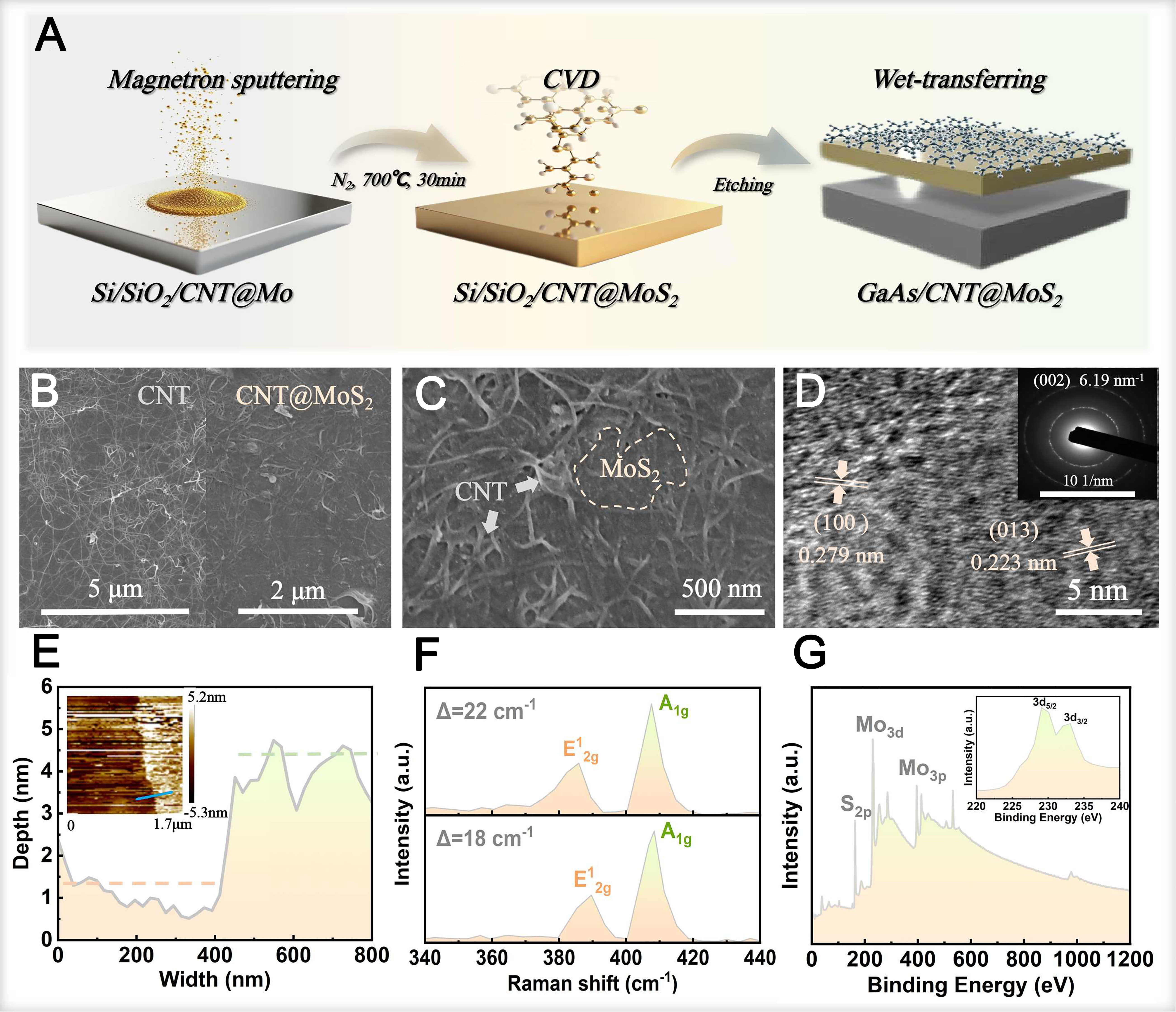
Figure 1. (A) Schematic of GaAs/CNT@MoS2 heterojunction; SEM images of (B) CNT film and (C) CNT@MoS2 film; (D) TEM images, (E) AFM images, (F) Raman and (G) XPS curves and the Mo 3d peaks (inserted curve) of the MoS2 film. GaAs: Gallium arsenide; CNT: carbon nanotube; TEM: transmission electron microscope; XPS: X-ray photoelectron spectroscopy; CVD: chemical vapor deposition; SEM: scanning electron microscope; AFM: atomic force microscope.
AFM analysis [Figure 1E] indicated local film thicknesses as low as 3 nm. These SEM and AFM results confirm the successful formation of a thin, continuous MoS2 layer atop the CNT network via the presented synthesis route. In the Raman spectrum of MoS2 [Figure 1F], the E12g mode at
X-ray photoelectron spectroscopy (XPS) was employed to probe the chemical states of the synthesized film [Figure 1G]. The survey spectrum is dominated by core-level signals from Mo and S. High-resolution scans reveal characteristic peaks at binding energies of 163.3, 229.3 and 233.1 eV, which are assigned to the S 2s, Mo 3d5/2, and Mo 3d3/2 levels, respectively. The doublet in the Mo 3d region, with a spin-orbit splitting of
To elucidate the energy band structure of the GaAs/CNT@MoS2 heterojunction, understanding the electronic properties of MoS2 films is crucial. The UPS spectrum of the MoS2 film [Figure 2A] exhibits distinct characteristic peaks within the 1.6-2.0 eV range, dominated by a strong peak centered at 1.93 eV. This energy aligns with the characteristic PL of monolayer MoS2[39,40] and is ascribed to radiative recombination of direct bandgap excitons, confirming a direct bandgap of 1.93 eV. Notably, in addition to the dominant 1.93 eV peak, a weak secondary peak emerges on the low-energy side, while a distinct shoulder peak structure is observed on the high-energy side. The weak low-energy peak is attributed to the coexistence of few-layer MoS2 within the film. Few-layer MoS2 possesses an indirect bandgap, necessitating phonon-assisted momentum compensation for PL to satisfy momentum conservation. Compared to the monolayer, few-layer MoS2 possesses an indirect bandgap, requiring phonon-assisted transitions that result in a redshifted and less intense emission. Additionally, defect-state-mediated electron-hole recombination within the bandgap may contribute to low-energy emission (with photon energy below the intrinsic bandgap). Conversely, a distinct shoulder on the high-energy flank originates from valence band (VB) splitting induced by strong spin-orbit coupling in MoS2.
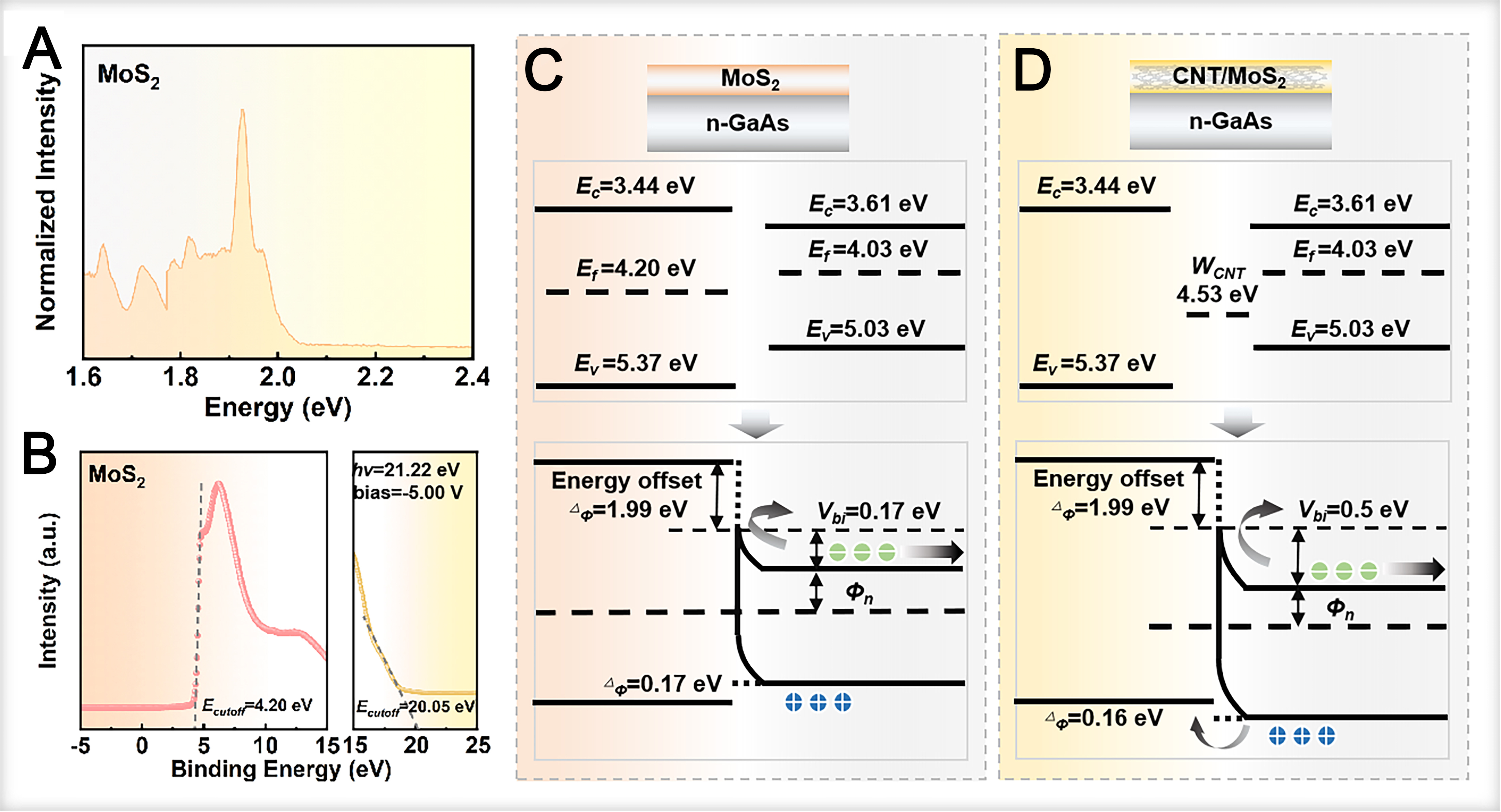
Figure 2. (A and B) UPS spectra of MoS2 film; (C and D) Energy band diagram of the GaAs heterojunction upon illumination. GaAs: Gallium arsenide; UPS: ultraviolet photoelectron spectroscopy; CNT: carbon nanotube.
To clarify the interfacial electronic properties, the secondary electron cutoff and VB region of the MoS2 film were analyzed by UPS [Figure 2B]. From these spectra, the work function (Φ) was determined to be 4.20 eV. The energy difference between the valence band maximum (VBM) and the Fermi level (Ef) was calculated to be 1.17 eV, derived using the incident photon energy (hν = 21.22 eV) and the secondary electron cutoff position (Ecutoff). The corresponding energy band diagrams for the GaAs/MoS2 and GaAs/CNT@MoS2 heterojunctions under illumination are illustrated in Figure 2C and D, respectively. Based on previous studies[31,32], the conduction band (Ec), Ef and valence band (EV) of GaAs are positioned at 3.61, 4.03 and
To further validate the inferred carrier transport behavior in the aforementioned heterojunction, the interfacial properties and electronic structure of the CNT@MoS2 system were investigated via theoretical simulations. The calculated partial density of states (PDOS) is presented in Supplementary Figure 2. As shown in Supplementary Figure 2A, the conduction band minimum (CBM) of MoS2 is dominated by S 3p states, whereas its VBM comprises hybridized both Mo 4d and S 3p states, indicating hybridization of electronic states between Mo and S atoms[41]. This hybridization is critical in defining the electronic properties of MoS2, including its bandgap and charge transport behavior. For the CNT component, PDOS analysis [Supplementary Figure 2B] indicates that electronic states near the Fermi level are predominantly derived from C 2p orbitals[42]. Furthermore, the finite density of states at the Fermi level [Supplementary Figure 2C] confirms the metallic character of the CNT, attributed to C 2p states crossing the Fermi level, which underpins its high electrical conductivity. To investigate interfacial charge transfer, GaAs/CNT and MoS2/CNT heterojunction models were constructed, and their charge transfer properties were calculated as presented in Supplementary Figure 2D and E.
In the charge density difference plot [Supplementary Figure 2D], the blue and red isosurfaces correspond to regions of electron depletion and accumulation, respectively. This distribution reveals a net electron transfer from the CNT side to the GaAs side at the GaAs/CNT interface. A similar charge transfer direction - from CNT to MoS2 - is observed in the MoS2/CNT heterojunction. For quantitative analysis, Mulliken charge distributions of the two heterojunctions were calculated (where the Mulliken charge value in Supplementary Figure 2E was set to an isovalue of 0.5 e/Å3). The analysis indicates a greater magnitude of charge redistribution at the GaAs-CNT interface than at the MoS2-CNT interface. These results collectively confirm that the overall charge transfer in the GaAs/CNT/MoS2 ternary heterojunction follows the trend of electron flow toward the GaAs side.
PV characteristics of GaAs@MoS2 heterojunction
Figure 3A and B presents the J-V characteristics of the devices based on CNT@MoS2 composite films with different CNT densities (0.01, 0.02 and 0.03 mg cm-2) under illumination and in the dark. The GaAs/CNT2@MoS2 heterojunction exhibits the optimal PV performance, with a short-circuit current density (Jsc) of 13.70 mA cm-2, an open-circuit voltage (Voc) of 0.65 V, a fill factor (FF) of 69.16%, and a PCE of 5.78%. This performance significantly outperforms that of GaAs/CNT1@MoS2 (3.42%) and GaAs/CNT3@MoS2 (4.56%). Notably, devices with lower CNT density exhibit a lower Jsc [Figure 3A], indicating that insufficient CNT content impedes efficient carrier transport. Conversely, at the excessive CNT density of 0.03 mg cm-2, a significant increase in the reverse saturation current density (J0) is observed [Figure 3B], which we attribute to CNT aggregation that reduces light absorption [Supplementary Figure 3] and enhances
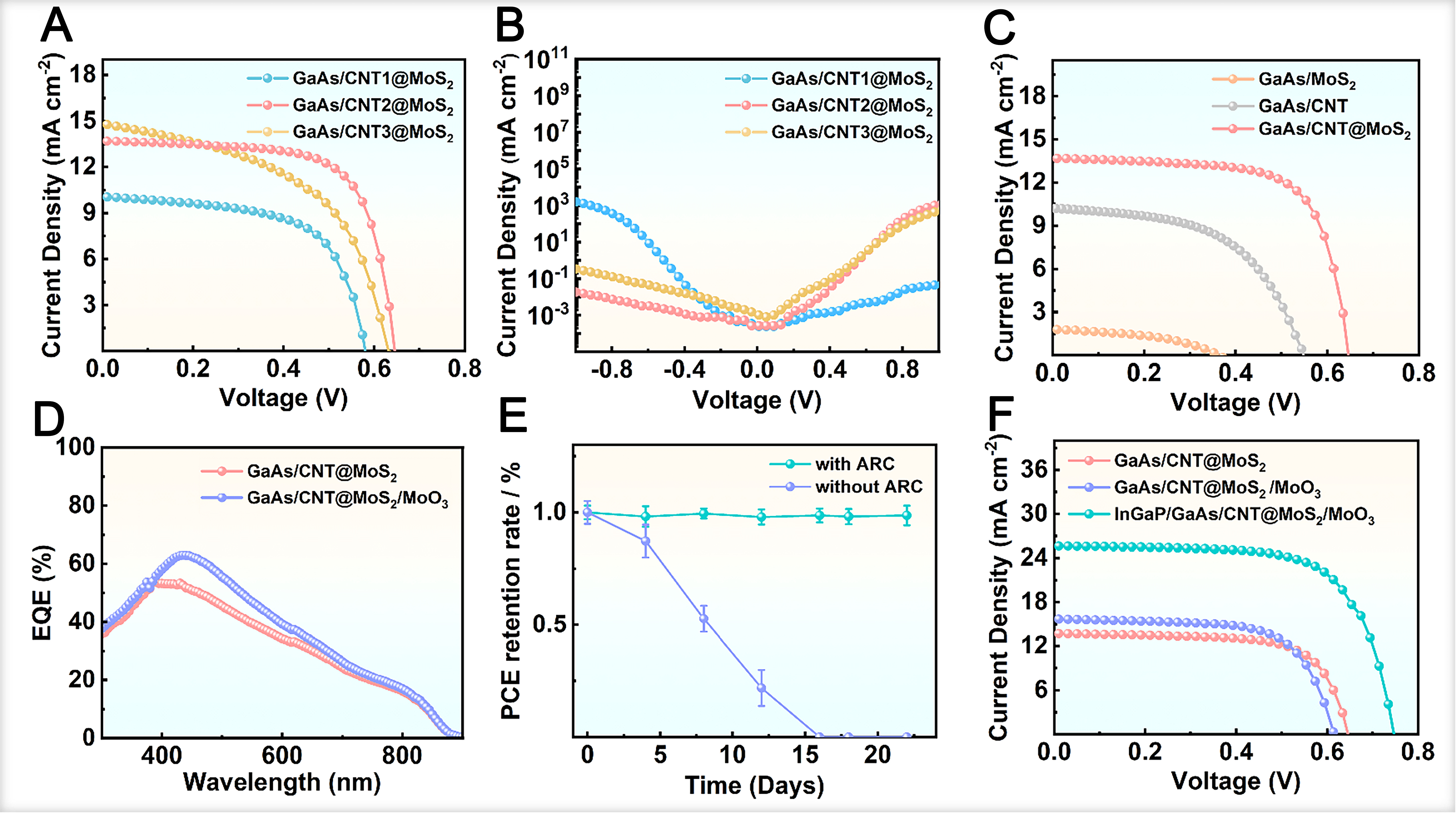
Figure 3. J-V characteristic of GaAs/CNT@MoS2 heterojunction under (A) illumination and (B) dark conditions; (C) J-V characteristic of GaAs/MoS2, GaAs/CNT and GaAs/CNT@MoS2 heterojunction; (D) EQE curves, (E) PCE retention and (F) J-V curves of GaAs/CNT@MoS2 heterojunction with/without MoO3 ARC. GaAs: Gallium arsenide; J-V: current density-voltage; CNT: carbon nanotube; EQE: external quantum efficiency; PCE: power conversion efficiency; ARC: anti-reflection coating.
A comparison of the PV parameters for the GaAs/CNT2@MoS2, GaAs/MoS2 and GaAs/CNT heterojunctions is summarized in Figure 3C. The GaAs/MoS2 device shows poor FF, Jsc and Voc, indicative of an inferior heterojunction quality where the band alignment is unfavorable for efficient carrier separation and the low conductivity of MoS2 limits charge extraction. GaAs/CNT heterojunctions exhibit improved band alignment, as fully validated in previous studies[16]. Nevertheless, the introduction of CNTs into the GaAs/MoS2 heterojunction results in an enhanced Jsc, affirming their role in promoting carrier separation and transport within the MoS2 film. The concurrent significant improvements in FF and Voc further verify the optimized heterojunction band alignment, consistent with the analysis presented in Figure 2D.
A key challenge for practical application is the environmental stability of the devices. Exposure to ambient air, particularly oxygen and water vapor, can lead to oxidation of MoS2-based structures and consequent performance degradation[43]. Meanwhile, the high light reflectivity of GaAs surface diminishes light absorption, posing another limitation for device performance[44]. To address these issues, focus was placed on introducing an anti-reflection coating (ARC) into the device structure. In this study, MoO3 was integrated into the device architecture. EQE tests [Figure 3D] reveal a pronounced integrated Jsc enhancement in the medium wavelength range of 400-600 nm. The sharp decline in EQE beyond 800 nm corresponds to the bandgap limitation of GaAs, where photons possess insufficient energy to generate electron-hole pairs. After confirming the stability of devices with MoO3 ARC, long-term PCE stability tests were performed on both ARC-containing and ARC-free devices in atmospheric environments. This result confirms that HJSCs with the ARC structure exhibited superior stability. The PCE of ARC-free devices rapidly decayed within the first few days, whereas that of ARC-containing devices remained relatively stable after three weeks, verifying that the MoO3 ARC possesses excellent encapsulation for heterojunction, effectively preventing the oxidation of GaAs hetero-interfaces in air and subsequent degradation in device stability [Figure 3E].
A comparison of the J-V characteristics [Figure 3F] demonstrates that the GaAs/CNT@MoS2/MoO3 HJSC achieves the highest PV performance, with a Jsc of 15.67 mA cm-2, an Voc of 0.62 V, an FF of 62.89%, and a PCE of 6.11%, outperforming GaAs/CNT@MoS2 (13.70 mA cm-2, 0.65 V, 69.16% and 5.78%). However, further efficiency gains are limited by carrier recombination at the back interface of GaAs, which is exacerbated by minority carrier flow. This challenge can be effectively mitigated by implementing a back surface field (BSF) structure, a strategy proven to enhance cell performance significantly[45]. An InGaP layer was selected as the BSF material due to its excellent lattice matching and comparable thermal expansion coefficient with GaAs, which minimizes the risk of wafer cracking from thermal stress and makes it an ideal candidate for GaAs-based HJSCs[46]. With the incorporation of the InGaP BSF, the device performance is substantially enhanced, yielding a Jsc of 25.61 mA cm-2, a Voc of 0.75 V, an FF of 68.71%, and a champion PCE of 12.41%.
Water splitting performance of GaAs/MoS2 heterojunction
Figure 4A schematically illustrates the working mechanism of the GaAs/CNT@MoS2 heterojunction as a photoelectrode in PEC water splitting. Under illumination, the CNT@MoS2 composite film acts as an efficient hole-transport layer, extracting photogenerated holes to the electrolyte interface for the oxygen evolution reaction (OER). Simultaneously, photogenerated electrons migrate through the GaAs substrate to the Pt counter electrode surface via an external circuit, where reduction reactions take place to produce hydrogen. On the RHE scale, the conduction band (CB) and VB of GaAs are located at -0.83 and 0.59 V, respectively. Photoinduced band bending resulting from the built-in potential (~0.7 V) shifts the effective CB and VB positions to -0.13 V and 1.29 V vs. RHE, respectively. This anodic shift raises the VB potential above the thermodynamic water oxidation potential (1.23 V vs. RHE), thereby facilitating efficient OER kinetics.
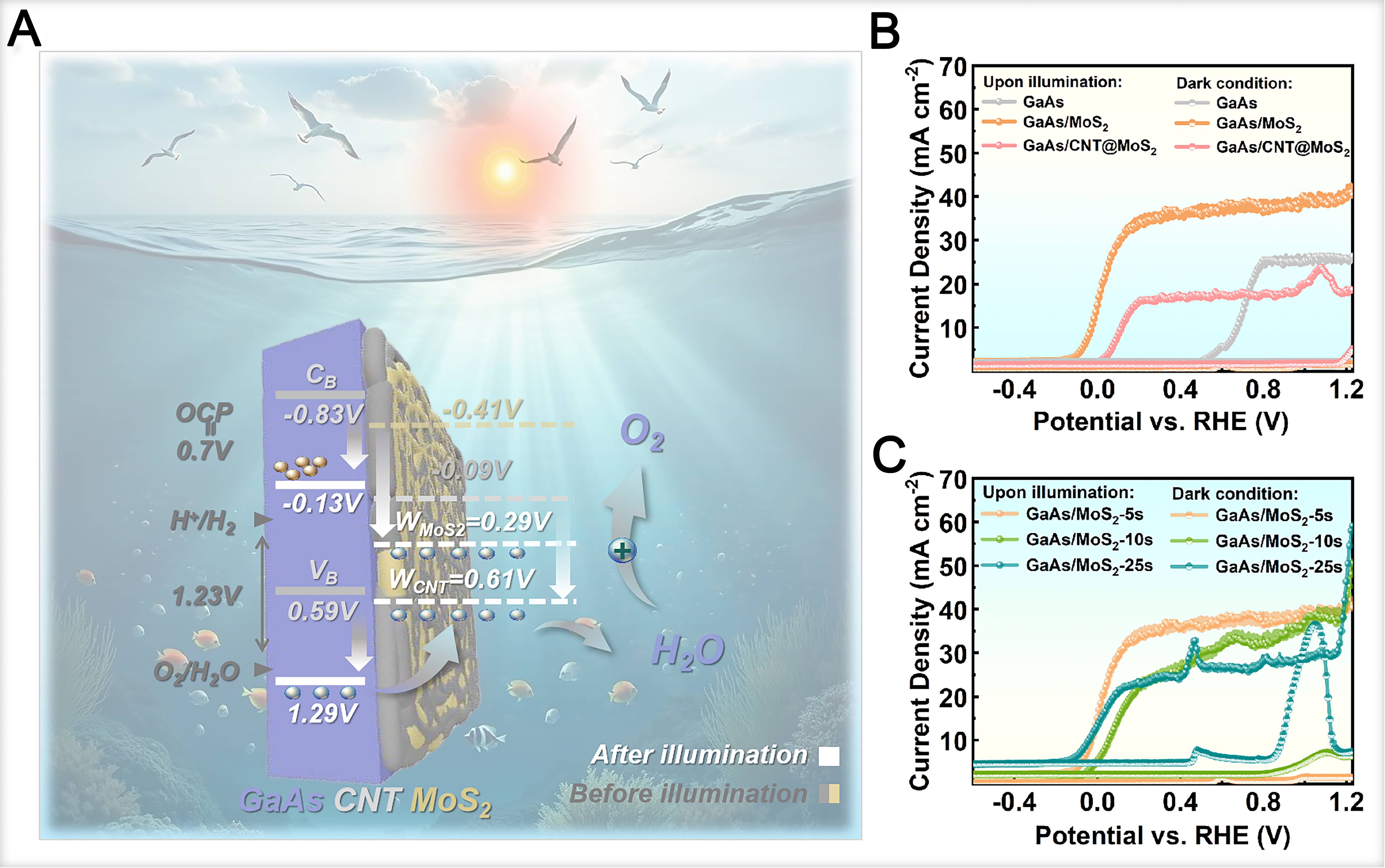
Figure 4. (A) PEC water splitting of GaAs/CNT@MoS2-based photoelectrodes upon illumination; (B) LSV curves of GaAs, GaAs/MoS2 and GaAs/CNT@MoS2 photoelectrodes; (C) LSV curves of GaAs/MoS2 photoelectrodes with different MoS2 thickness. GaAs: Gallium arsenide; CNT: carbon nanotube; PEC: photoelectrochemical; LSV: linear sweep voltammetry; OCP: open-circuit potential; RHE: reversible hydrogen electrode.
Figure 4B shows linear sweep voltammetry (LSV) curves of GaAs, GaAs/MoS2 and GaAs/CNT@MoS2 heterojunction photoelectrodes. All samples exhibit a negligible J0. The GaAs/MoS2 photoanode displays the highest Jsc compared to GaAs and GaAs/CNT@MoS2. Additionally, GaAs/MoS2 shows a more negative shift in onset potential than the other two groups, demonstrating a superior PV response. Thus, GaAs/MoS2 was selected for self-driven PEC water splitting research. Figure 4C compares the LSV curves of GaAs/MoS2 photoelectrodes with varying MoS2 thicknesses. The GaAs/MoS2-5s sample shows a stable, near-zero J0 across the measured potential range. In contrast, samples with thicker MoS2 layers (e.g., MoS2-10s,
The ABPE was measured to evaluate the STH conversion efficiency of the photoelectrodes, as summarized in Figure 5A. The GaAs/MoS2 heterojunctions demonstrate substantially enhanced ABPE values compared to the bare GaAs control, with the performance being highly dependent on the MoS2 thickness. The
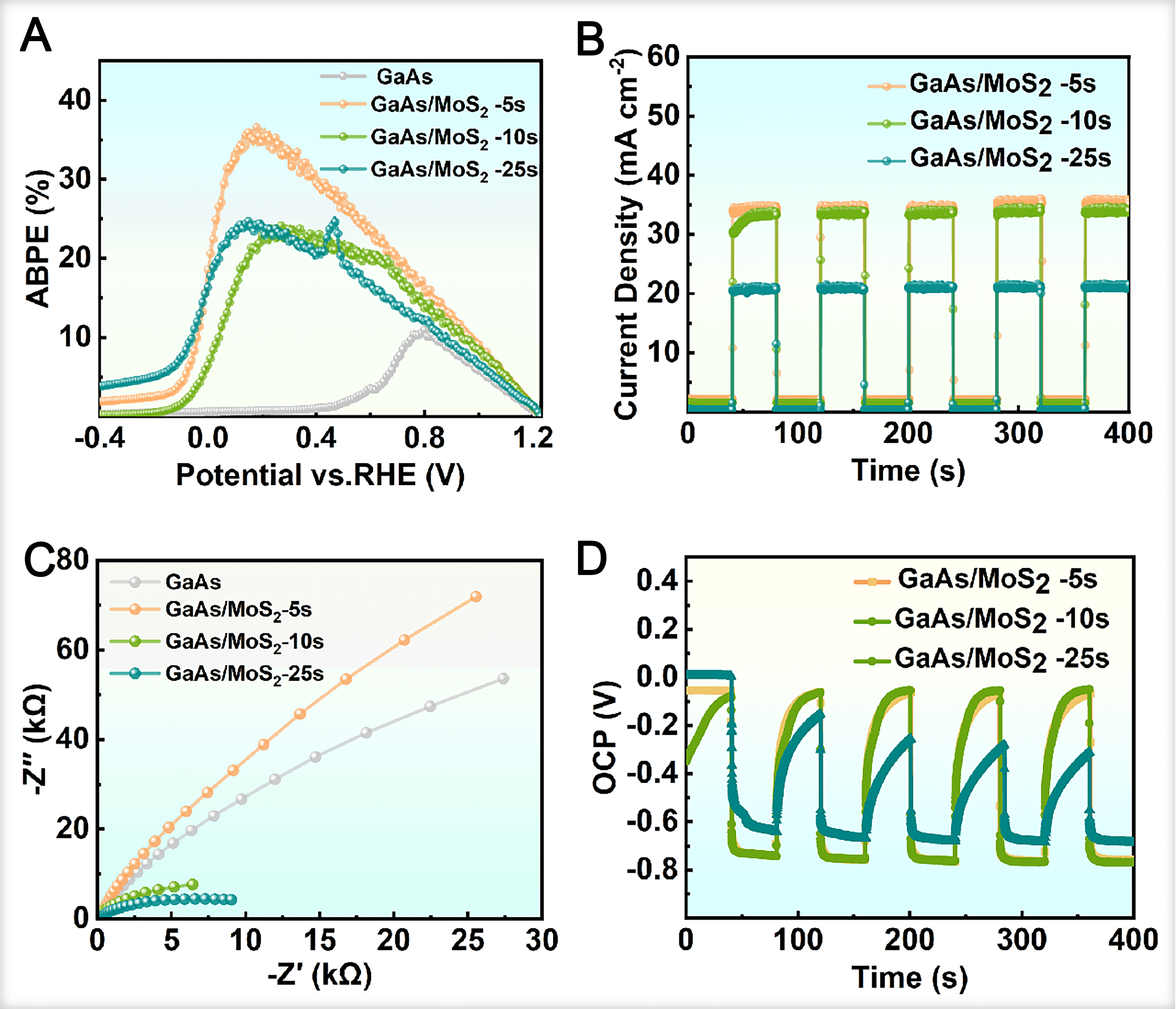
Figure 5. (A) ABPE plots; (B) Chopping J-t curves; (C) EIS Nyquist plots at 1.23 V vs. RHE under dark conditions; (D) OCP curves of the GaAs/MoS2 photoanodes with different MoS2 thicknesses. GaAs: Gallium arsenide; ABPE: applied bias photon-to-current efficiency; J-t: current density-time; EIS: electrochemical impedance spectroscopy; RHE: reversible hydrogen electrode; OCP: open-circuit potential.
Chopped voltammetry analysis [Figure 5B] shows that the stable photocurrent response of all samples over multiple on-off illumination cycles, indicating robust operational stability. Meanwhile, the GaAs/MoS2-5s photoanode exhibits the highest photocurrent density and the most rapid response kinetics, directly demonstrating that an optimal MoS2 film thickness enhances charge transfer at the electrode-electrolyte interface. To gain further insight into the interfacial charge transfer processes, electrochemical impedance spectroscopy (EIS) was performed [Figure 5C]. Analysis of the semicircle diameter and slope in the EIS curves yields information regarding the interfacial charge transfer resistance (RCT) and ion diffusion characteristics[47]. Notably, the absence of distinct semicircles in the EIS curves of all samples in acidic electrolyte indicates good charge transfer capability. However, only the curve slope of the GaAs/MoS2-5s photoanode is significantly larger than that of the GaAs control group. As the MoS2 film thickness increases, the slope decreases markedly, eventually falling below that of the control sample. This trend indicates that excessively thick MoS2 films hinder ion diffusion and charge transport at the film-electrolyte interface, which is consistent with the photocurrent measurements.
Open-circuit potential (OCP) measurements provide further insight into the photoelectrode performance. By measuring the OCP of the photoelectrode before and after illumination, it can not only directly reflect its photoresponse capability but also be used to analyze the trap state density in the material[48]. The OCP was monitored over an extended period prior to illumination to assess the intrinsic stability of the electrode
To further evaluate the operational stability of the GaAs/MoS2-5s heterojunction for PEC water splitting, chronoamperometric measurements were conducted over 150 min under continuous illumination
As illustrated in Figure 6A, a PV-coupled PEC water splitting system was constructed by integrating the InGaP/GaAs/CNT@MoS2/MoO3 HJSC with the GaAs/MoS2 photoelectrode. In this integrated system, the GaAs/MoS2-based HJSC and GaAs/MoS2 photoelectrode are connected in series. The top electrode of the HJSC is connected to the photoanode via a wire, and the back electrode is connected to the Pt electrode, thereby closing the circuit. This integrated design simultaneously harnesses the electrical output from the HJSC and the PEC activity of the GaAs/MoS2 photoanode, enabling unassisted (bias-free) solar water splitting.
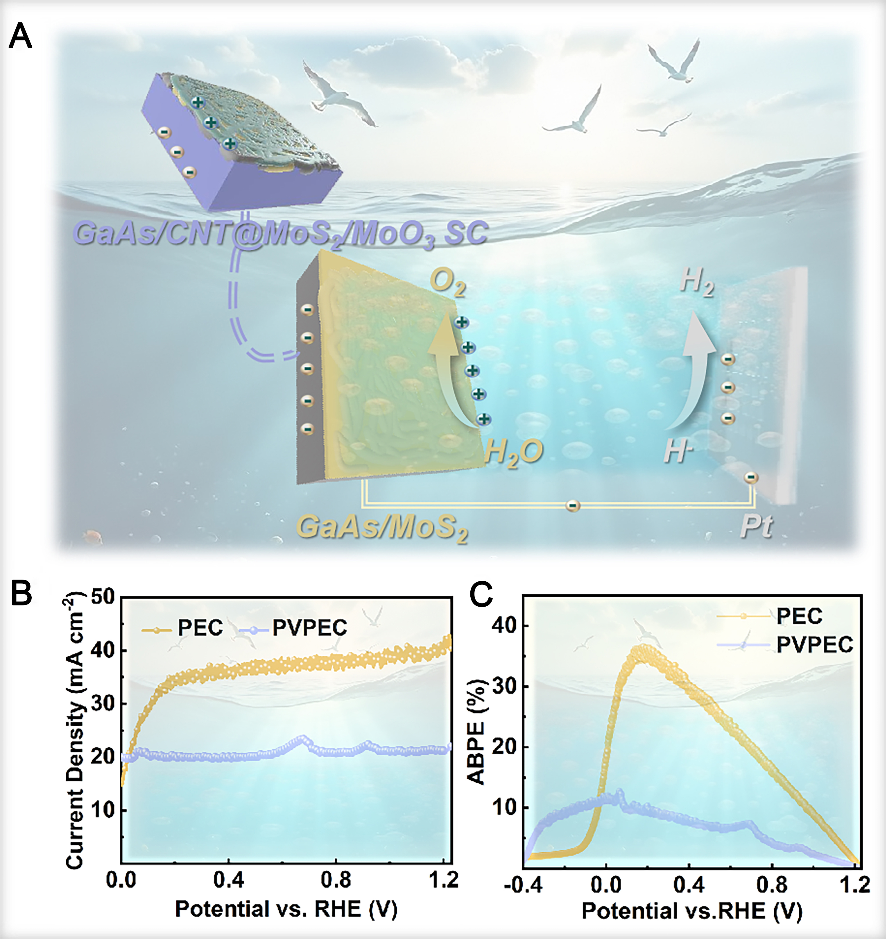
Figure 6. (A) PEC water splitting of GaAs/CNT@MoS2-based photoelectrodes combined with GaAs/CNT@MoS2/MoO3 heterojunction solar cells upon illumination; (B) LSV curves and (C) ABPE plots of PEC and PVEC systems, respectively. GaAs: Gallium arsenide; ABPE: applied bias photon-to-current efficiency; CNT: carbon nanotube; LSV: linear sweep voltammetry; PEC: photoelectrochemical; PVPEC: photovoltaic-photoelectrochemical; RHE: reversible hydrogen electrode; SC: solar cell.
The integrated PV-PEC system was subsequently evaluated under illumination, with the corresponding LSV and ABPE curves presented in Figure 6B and C, respectively. A significant photocurrent density is observed at 0 V vs. RHE, confirming efficient charge separation and migration driven by the high-performance GaAs/MoS2 photoanode. The stability of the current density curve indicates that the HJSC provides a sufficient operating potential, while the overall current output appears to be limited by either the electrocatalytic activity at the electrode/electrolyte interface or the maximum photocurrent deliverable by the HJSC itself. Notably, the integration of the GaAs HJSC induces a substantial cathodic shift of approximately 400 mV in the water oxidation onset potential. This reduction in the overpotential requirement lowers the dependence on an external electrical bias and decreases the overall energy consumption of the system.
However, the overall efficiency of the integrated system is compromised. Although the current density of
This study primarily focuses on the sequential development from “material-heterojunction structure-photoelectrode and device”. To address the high cost, corrosion susceptibility, and poor stability of traditional GaAs photoelectrodes, the preparation of novel hole-transport layers and their GaAs heterojunctions is pivotal for reducing costs, which is crucial for industrialization. Cost-control technologies at the material level directly lower the barrier to large-scale hydrogen production using high-performance III-V semiconductors. Concurrently, rational heterojunction structure design effectively promotes the separation and extraction of photogenerated carriers, optimizes interfacial band alignment, and reduces the overpotential required for the PEC reaction. Investigating such a precise band structure and interface engineering deepens our understanding of the charge transfer mechanism at the solid-liquid interface, representing a significant advancement in the fundamental research of PV devices. Furthermore, this work extends beyond the optimization of individual photoelectrodes by achieving the synergistic integration of photoelectrodes with SCs. This simplified, monolithic system design eliminates the dependency of conventional electrolyzers on external PV power plants and the electrical grid. It is more suitable for modular deployment and reduces installation and maintenance costs, representing a critical step towards distributed and scalable solar hydrogen production facilities.
CONCLUSIONS
In summary, this study successfully fabricated GaAs/MoS2 heterojunction photoelectrodes through vacuum filtration, magnetron sputtering, and CVD techniques, achieving breakthrough progress in PEC water splitting performance and the development of an integrated self-driven solar water splitting system. By incorporating a CNT hole transport layer, MoO3 ARC and InGaP BSF, the PCE was significantly enhanced from 5.78% to 12.41%, along with excellent operational stability. The GaAs/MoS2 photoelectrode exhibited superior PV response characteristics, demonstrating a more negative onset potential shift and higher Jsc. The optimized GaAs/MoS2 photoelectrode achieved an exceptional photocurrent density of 40 mA cm-2, maintaining an ABPE of 20% at 0 V vs. RHE, and reaching a maximum ABPE of 35% under bias. The integrated PV-PEC system delivered a sustained current density of 20 mA cm-2 at 0 V vs. RHE, confirming its highly efficient self-driven water splitting capability. By leveraging the GaAs HJSC to provide a stable potential, this synergistic system significantly reduces dependence on external power sources, offering an innovative solution for developing self-sustained, green hydrogen production technologies.
DECLARATIONS
Acknowledgments
This work was supported by South China University of Technology and Wuyi University, which facilitated the cross-institutional research efforts described in this paper, and we are grateful to Dr. Zhong, Dr. Lin and Prof. Li for their insightful comments and guidance during the experimental design phase.
Authors’ contributions
Made substantial contributions to conception and design of the study and performed data analysis and interpretation: Mo, Y.; Liu, P.
Performed data acquisition and provided administrative, technical, and material support: Chen, F.; Zhang, H.; Huan, T.; He, Q.; Yuan, C.; Yang, Y.; Xiao, M.
Proposed and supervised the project and reviewed the manuscript: Zhong, J. X.; Lin, J.; Li, G.
Availability of data and materials
Some results of supporting the study are presented in the Supplementary Materials. Other raw data that support the findings of this study are available from the corresponding author upon reasonable request.
Financial support and sponsorship
This work was supported by the National Natural Science Foundation of China (52302169), Guangzhou Science and Technology Plan (2025A04J3365), Key Scientific Research Projects of General Universities in Guangdong Province (2023KTSCX095), Research and Innovation Group of Guangdong University of Education (2024KYCXTD014), and Guangdong Basic and Applied Basic Research Foundation (2023A1515011208).
Conflicts of interest
All authors declared that there are no conflicts of interest.
Ethical approval and consent to participate
Not applicable.
Consent for publication
Not applicable.
Copyright
© The Author(s) 2025.
Supplementary Materials
REFERENCES
1. Zhao, Y.; Niu, Z.; Zhao, J.; Xue, L.; Fu, X.; Long, J. Recent advancements in photoelectrochemical water splitting for hydrogen production. Electrochem. Energy. Rev. 2023, 6, 14.
2. Dong, Z.; Chen, M.; Qin, D.; Han, S. Recent advances and perspective of modified TiO2-based photoanodes toward photoelectrochemical water splitting. Fuel 2024, 373, 132366.
3. Su, Y.; Yu, W.; Liao, L.; et al. Unveiling the synergy of interfacial contact and defects in α-Fe2O3 for enhanced photo-electrochemical water splitting. Adv. Funct. Mater. 2023, 33, 2303976.
4. Gonçalves, S.; Quitério, P.; Freitas, J.; et al. Unveiling morphology-structure interplay on hydrothermal WO3 nanoplatelets for photoelectrochemical solar water splitting. ACS. Appl. Mater. Interfaces. 2024, 16, 64389-409.
5. Gaikwad, M. A.; Suryawanshi, U. P.; Ghorpade, U. V.; Jang, J. S.; Suryawanshi, M. P.; Kim, J. H. Emerging surface, bulk, and interface engineering strategies on BiVO4 for photoelectrochemical water splitting. Small 2022, 18, 2105084.
6. Das, A.; Devasia, S.; Banerjee, N.; Nair, R. G. High aspect ratio ZnO nanorods for improved photoelectrochemical (PEC) water splitting performances and efficient photocatalytic hydrogen evolution: an integrated experimental and DFT studies. Appl. Surf. Sci. 2025, 699, 163160.
7. Fu, J.; Fan, Z.; Nakabayashi, M.; et al. Interface engineering of Ta3N5 thin film photoanode for highly efficient photoelectrochemical water splitting. Nat. Commun. 2022, 13, 729.
8. Hojamberdiev, M.; Vargas, R.; Zhang, F.; Teshima, K.; Lerch, M. Perovskite BaTaO2N: from materials synthesis to solar water splitting. Adv. Sci. 2023, 10, 2305179.
9. Shabbir, S. A.; Ali, I.; Haris, M.; et al. Bifunctional Co3O4/g-C3N4 hetrostructures for photoelectrochemical water splitting. ACS. Omega. 2024, 9, 21450-8.
10. Teitsworth, T. S.; Hill, D. J.; Litvin, S. R.; et al. Water splitting with silicon p-i-n superlattices suspended in solution. Nature 2023, 614, 270-4.
11. Wang, T.; Wang, Y.; Liu, Y.; et al. Construction of Z-type In2O3@InP heterostructure with enhanced photo-assisted electrocatalytic water splitting for hydrogen production. Int. J. Hydrogen. Energy. 2024, 64, 166-77.
12. Alotaibi, A. M.; Muayqil, E.; Al Abass, N.; et al. Surface engineering of CuO-Cu2O heterojunction thin films for improved photoelectrochemical water splitting. Renew. Energy. 2024, 235, 121326.
13. Cai, Y.; Wang, S.; Liu, B.; et al. Semi-transparent and stable In2S3/CdTe heterojunction photoanodes for unbiased photoelectrochemical water splitting. Nat. Commun. 2025, 16, 5105.
14. Štěpánek, J.; Bystron, T.; Paušová, Š. Two-step synthesis and characterization of CuFeO2 thin layers for photoelectrocatalytic applications. Electrochimica. Acta. 2025, 535, 146516.
15. Wang, Z.; Zhu, H.; Tu, W.; et al. Host/guest nanostructured photoanodes integrated with targeted enhancement strategies for photoelectrochemical water splitting. Adv. Sci. 2022, 9, 2103744.
16. Kang, J.; Yoon, K.; Lee, J.; Park, J.; Chaule, S.; Jang, J. Meso-pore generating P doping for efficient photoelectrochemical water splitting. Nano. Energy. 2023, 107, 108090.
17. Yuan, H.; Zhang, Y.; Su, Y.; et al. A novel BiVO4/DLC heterojunction for efficient photoelectrochemical water splitting. Chem. Eng. J. 2023, 459, 141637.
18. Li, C.; Xiao, J.; Jia, X.; Zhao, Q.; Du, B.; Wang, B. Unveiling the influence of lower-valence Ni in hydroxide Co-catalyst and attaining efficient photoanodes with FeOOH holes transfer layer for photoelectrochemical water splitting. Adv. Funct. Mater. 2025, 35, 2406999.
19. Mo, Y.; Deng, X.; Liu, P.; Guo, J.; Wang, W.; Li, G. Insights into the application of carbon materials in heterojunction solar cells. Mater. Sci. Eng. R. Rep. 2023, 152, 100711.
20. Zhang, X.; Lu, G.; Ning, X.; Wang, C. Boron substitution enhanced activity of BxGa1-xAs/GaAs photocatalyst for water splitting. Appl. Catal. B. Environ. 2022, 300, 120690.
21. Kang, D.; Young, J. L.; Lim, H.; et al. Printed assemblies of GaAs photoelectrodes with decoupled optical and reactive interfaces for unassisted solar water splitting. Nat. Energy. 2017, 2, 17043.
22. Vu TK, Tran MT, Kim EK. Optimization of active antireflection ZnO films for p-GaAs-based heterojunction solar cells. J. Alloys. Compd. 2022, 924, 166531.
23. Wang, J.; Guo, J.; Liang, J.; et al. InP QDs modified GaAs/PEDOT:PSS hybrid solar cell with efficiency over 15%. Nano. Lett. 2024, 24, 12111-7.
24. Lin, S.; Li, X.; Wang, P.; et al. Interface designed MoS2/GaAs heterostructure solar cell with sandwich stacked hexagonal boron nitride. Sci. Rep. 2015, 5, 15103.
25. Haggren, T.; Raj, V.; Haggren, A.; Gagrani, N.; Jagadish, C.; Tan, H. CuI as a hole-selective contact for GaAs solar cells. ACS. Appl. Mater. Interfaces. 2022, 14, 52918-26.
26. Wen, L.; Gao, F.; Yu, Y.; et al. Enhancing the photovoltaic performance of GaAs/graphene Schottky junction solar cells by interfacial modification with self assembled alkyl thiol monolayer. J. Mater. Chem. A. 2018, 6, 17361-70.
27. Li, X.; Chen, W.; Zhang, S.; et al. 18.5% efficient graphene/GaAs van der Waals heterostructure solar cell. Nano. Energy. 2015, 16, 310-9.
28. Chen, Y.; Shi, X.; Zhou, D.; et al. Highly efficient SWCNT/GaAs van der Waals heterojunction solar cells enhanced by Nafion doping. J. Alloys. Compd. 2023, 932, 167624.
29. Tan, X.; Cen, W.; Qian, G.; Chen, Q.; Xie, Q. The GaAs/InS vdW heterostructure shows great potential as a solar-driven water splitting photocatalyst. Mater. Sci. Semicond. Process. 2023, 167, 107779.
30. Arunachalam, M.; Kanase, R. S.; Zhu, K.; Kang, S. H. Reliable bi-functional nickel-phosphate/TiO2 integration enables stable n-GaAs photoanode for water oxidation under alkaline condition. Nat. Commun. 2023, 14, 5429.
31. Mo, Y.; Xie, S.; Huang, T.; et al. Self-integrated carbon nanotube/graphene oxide-based GaAs heterojunction synergistically achieve unassisted water splitting with solar-to-hydrogen efficiency over 15%. Chem. Eng. J. 2025, 519, 164889.
32. Mo, Y.; Guo, C.; Wang, W.; et al. Interface passivation treatment enables GaAs/CNT heterojunction solar cells over 19 % efficiency. Nano. Energy. 2024, 131, 110247.
33. Xia, Y.; Chen, X.; Wei, J.; et al. 12-inch growth of uniform MoS2 monolayer for integrated circuit manufacture. Nat. Mater. 2023, 22, 1324-31.
34. Zhu, Z.; Tang, Y.; Leow, W. R.; et al. Approaching the lithiation limit of MoS2 while maintaining its layered crystalline structure to improve lithium storage. Angew. Chem. Int. Ed. 2019, 58, 3521-6.
35. Mouri, S.; Miyauchi, Y.; Matsuda, K. Tunable photoluminescence of monolayer MoS2 via chemical doping. Nano. Lett. 2013, 13, 5944-8.
36. Benoist, L. XPS analysis of oxido-reduction mechanisms during lithium intercalation in amorphous molybdenum oxysulfide thin films. Solid. State. Ionics. 1995, 76, 81-9.
37. Zhang, Y.; Sun, Y.; Zhong, B. Synthesis of higher alcohols from syngas over ultrafine Mo-Co-K catalysts. Catal. Lett. 2001, 76, 249-53.
38. Tsuboi, Y.; Wang, F.; Kozawa, D.; et al. Enhanced photovoltaic performances of graphene/Si solar cells by insertion of a MoS2 thin film. Nanoscale 2015, 7, 14476-82.
39. Mak, K. F.; Lee, C.; Hone, J.; Shan, J.; Heinz, T. F. Atomically thin MoS2: a new direct-gap semiconductor. Phys. Rev. Lett. 2010, 105, 136805.
40. Frey, G. L.; Elani, S.; Homyonfer, M.; Feldman, Y.; Tenne, R. Optical-absorption spectra of inorganic fullerenelike MS2 ( M=Mo, W). Phys. Rev. B. 1998, 57, 6666.
41. Komesu, T.; Le, D.; Ma, Q.; et al. Symmetry-resolved surface-derived electronic structure of MoS2(0 0 0 1). J. Phys. Condens. Matter. 2014, 26, 455501.
42. Zhao, C.; Zhou, X.; Xie, S.; et al. DFT study of electronic structure and properties of N, Si and Pd-doped carbon nanotubes. Ceram. Int. 2018, 44, 21027-33.
43. Lee, G. H.; Cui, X.; Kim, Y. D.; et al. Highly stable, dual-gated MoS2 transistors encapsulated by hexagonal boron nitride with gate-controllable contact, resistance, and threshold voltage. ACS. Nano. 2015, 9, 7019-26.
44. Ding, K.; Zhang, X.; Ning, L.; et al. Hue tunable, high color saturation and high-efficiency graphene/silicon heterojunction solar cells with MgF2/ZnS double anti-reflection layer. Nano. Energy. 2018, 46, 257-65.
45. Abbasian, S.; Sabbaghi-nadooshan, R. Optimum design of ARC-less InGaP/GaAs DJ solar cell with hetero tunnel junction. J. Electron. Mater. 2018, 47, 3585-95.
46. Hemani, A.; Dennai, B.; Nouri, A.; Khachab, H.; Dekkich, B. Effect of the FSF and BSF layers on the performances of the GaAs solar cell. J. Ovonic. Res. 2017, 13, 307-14. https://chalcogen.ro/307_AbderrahmaneH.pdf (accessed 2025-11-24).
47. Siavash, Moakhar. R.; Hosseini-Hosseinabad, S. M.; Masudy-Panah, S.; et al. Photoelectrochemical water-splitting using CuO-based electrodes for hydrogen production: a review. Adv. Mater. 2021, 33, 2007285.
48. Chen, W.; Buyanova, I.; Tu, C.; Yonezu, H. Point defects in dilute nitride III-N-As and III-N-P. Phy. B. Condens. Matter. 2006, 376-7, 545-51.
49. Meng, X.; Li, Z.; Liu, Y.; et al. Enabling unassisted solar water splitting with concurrent high efficiency and stability by robust earth-abundant bifunctional electrocatalysts. Nano. Energy. 2023, 109, 108296.
50. Butson, J. D.; Sharma, A.; Chen, H.; et al. Surface-structured cocatalyst foils unraveling a pathway to high-performance solar water splitting. Adv. Energy. Mater. 2022, 12, 2102752.
51. Sun, K.; Liu, R.; Chen, Y.; Verlage, E.; Lewis, N. S.; Xiang, C. A stabilized, intrinsically safe, 10% efficient, solar-driven water-splitting cell incorporating earth-abundant electrocatalysts with steady-state pH gradients and product separation enabled by a bipolar membrane. Adv. Energy. Mater. 2016, 6, 1600379.
Cite This Article
How to Cite
Download Citation
Export Citation File:
Type of Import
Tips on Downloading Citation
Citation Manager File Format
Type of Import
Direct Import: When the Direct Import option is selected (the default state), a dialogue box will give you the option to Save or Open the downloaded citation data. Choosing Open will either launch your citation manager or give you a choice of applications with which to use the metadata. The Save option saves the file locally for later use.
Indirect Import: When the Indirect Import option is selected, the metadata is displayed and may be copied and pasted as needed.
About This Article
Copyright

Data & Comments
Data
0


Comments
Comments must be written in English. Spam, offensive content, impersonation, and private information will not be permitted. If any comment is reported and identified as inappropriate content by OAE staff, the comment will be removed without notice. If you have any queries or need any help, please contact us at [email protected].